EP1717201B1 - Moule, procede de formation de celui-ci, et procede de production d'un substrat en silicium polycristallin utilisant ce moule - Google Patents
Moule, procede de formation de celui-ci, et procede de production d'un substrat en silicium polycristallin utilisant ce moule Download PDFInfo
- Publication number
- EP1717201B1 EP1717201B1 EP05704366A EP05704366A EP1717201B1 EP 1717201 B1 EP1717201 B1 EP 1717201B1 EP 05704366 A EP05704366 A EP 05704366A EP 05704366 A EP05704366 A EP 05704366A EP 1717201 B1 EP1717201 B1 EP 1717201B1
- Authority
- EP
- European Patent Office
- Prior art keywords
- mold
- lateral surface
- members
- surface member
- surface members
- Prior art date
- Legal status (The legal status is an assumption and is not a legal conclusion. Google has not performed a legal analysis and makes no representation as to the accuracy of the status listed.)
- Expired - Lifetime
Links
- 238000000034 method Methods 0.000 title claims description 57
- 229910021420 polycrystalline silicon Inorganic materials 0.000 title claims description 25
- 239000000758 substrate Substances 0.000 title claims description 20
- 238000004519 manufacturing process Methods 0.000 title description 14
- XUIMIQQOPSSXEZ-UHFFFAOYSA-N Silicon Chemical compound [Si] XUIMIQQOPSSXEZ-UHFFFAOYSA-N 0.000 claims description 134
- 229910052710 silicon Inorganic materials 0.000 claims description 133
- 239000010703 silicon Substances 0.000 claims description 133
- 239000000463 material Substances 0.000 claims description 51
- 238000003825 pressing Methods 0.000 claims description 45
- 230000002093 peripheral effect Effects 0.000 claims description 17
- 238000006073 displacement reaction Methods 0.000 claims description 11
- 238000001035 drying Methods 0.000 claims description 3
- VYPSYNLAJGMNEJ-UHFFFAOYSA-N Silicium dioxide Chemical compound O=[Si]=O VYPSYNLAJGMNEJ-UHFFFAOYSA-N 0.000 description 31
- OKTJSMMVPCPJKN-UHFFFAOYSA-N Carbon Chemical compound [C] OKTJSMMVPCPJKN-UHFFFAOYSA-N 0.000 description 22
- 238000002844 melting Methods 0.000 description 19
- 230000008018 melting Effects 0.000 description 19
- 238000001816 cooling Methods 0.000 description 17
- 229910002804 graphite Inorganic materials 0.000 description 17
- 239000010439 graphite Substances 0.000 description 17
- 238000005304 joining Methods 0.000 description 17
- 238000005266 casting Methods 0.000 description 16
- 239000002994 raw material Substances 0.000 description 15
- 229910052581 Si3N4 Inorganic materials 0.000 description 13
- 239000000377 silicon dioxide Substances 0.000 description 13
- HQVNEWCFYHHQES-UHFFFAOYSA-N silicon nitride Chemical compound N12[Si]34N5[Si]62N3[Si]51N64 HQVNEWCFYHHQES-UHFFFAOYSA-N 0.000 description 13
- 238000010438 heat treatment Methods 0.000 description 11
- 230000008569 process Effects 0.000 description 9
- 239000004065 semiconductor Substances 0.000 description 9
- 235000012239 silicon dioxide Nutrition 0.000 description 9
- XKRFYHLGVUSROY-UHFFFAOYSA-N Argon Chemical compound [Ar] XKRFYHLGVUSROY-UHFFFAOYSA-N 0.000 description 8
- 230000000694 effects Effects 0.000 description 8
- 239000000155 melt Substances 0.000 description 8
- 239000000843 powder Substances 0.000 description 6
- 230000003252 repetitive effect Effects 0.000 description 6
- 238000007711 solidification Methods 0.000 description 6
- 230000008023 solidification Effects 0.000 description 6
- 239000003575 carbonaceous material Substances 0.000 description 5
- 238000005520 cutting process Methods 0.000 description 5
- 239000011810 insulating material Substances 0.000 description 5
- 239000010453 quartz Substances 0.000 description 5
- 230000001105 regulatory effect Effects 0.000 description 5
- 239000004372 Polyvinyl alcohol Substances 0.000 description 4
- 229910052786 argon Inorganic materials 0.000 description 4
- 229910052799 carbon Inorganic materials 0.000 description 4
- 229920002451 polyvinyl alcohol Polymers 0.000 description 4
- 239000002002 slurry Substances 0.000 description 4
- 239000011248 coating agent Substances 0.000 description 3
- 238000000576 coating method Methods 0.000 description 3
- 238000010586 diagram Methods 0.000 description 3
- 239000012535 impurity Substances 0.000 description 3
- 229910021421 monocrystalline silicon Inorganic materials 0.000 description 3
- 230000009467 reduction Effects 0.000 description 3
- 239000006061 abrasive grain Substances 0.000 description 2
- 238000006243 chemical reaction Methods 0.000 description 2
- 229910021419 crystalline silicon Inorganic materials 0.000 description 2
- 239000007770 graphite material Substances 0.000 description 2
- 230000006698 induction Effects 0.000 description 2
- 239000010410 layer Substances 0.000 description 2
- 239000007788 liquid Substances 0.000 description 2
- 239000000203 mixture Substances 0.000 description 2
- 238000000465 moulding Methods 0.000 description 2
- 239000003921 oil Substances 0.000 description 2
- HBMJWWWQQXIZIP-UHFFFAOYSA-N silicon carbide Chemical compound [Si+]#[C-] HBMJWWWQQXIZIP-UHFFFAOYSA-N 0.000 description 2
- 229910010271 silicon carbide Inorganic materials 0.000 description 2
- 239000007787 solid Substances 0.000 description 2
- XLYOFNOQVPJJNP-UHFFFAOYSA-N water Substances O XLYOFNOQVPJJNP-UHFFFAOYSA-N 0.000 description 2
- 239000000853 adhesive Substances 0.000 description 1
- 230000001070 adhesive effect Effects 0.000 description 1
- 230000008859 change Effects 0.000 description 1
- 150000001875 compounds Chemical class 0.000 description 1
- 230000001276 controlling effect Effects 0.000 description 1
- 239000002826 coolant Substances 0.000 description 1
- 239000002173 cutting fluid Substances 0.000 description 1
- 230000007547 defect Effects 0.000 description 1
- 229920006332 epoxy adhesive Polymers 0.000 description 1
- 239000007789 gas Substances 0.000 description 1
- 239000011521 glass Substances 0.000 description 1
- 239000002184 metal Substances 0.000 description 1
- 239000007769 metal material Substances 0.000 description 1
- 238000002156 mixing Methods 0.000 description 1
- 229910052755 nonmetal Inorganic materials 0.000 description 1
- 239000002245 particle Substances 0.000 description 1
- 239000011819 refractory material Substances 0.000 description 1
- 238000005057 refrigeration Methods 0.000 description 1
- 229920005989 resin Polymers 0.000 description 1
- 239000011347 resin Substances 0.000 description 1
- 230000000452 restraining effect Effects 0.000 description 1
- 238000005204 segregation Methods 0.000 description 1
- 229910021422 solar-grade silicon Inorganic materials 0.000 description 1
- 238000003892 spreading Methods 0.000 description 1
- 230000007480 spreading Effects 0.000 description 1
- 239000002344 surface layer Substances 0.000 description 1
Images






Classifications
-
- B—PERFORMING OPERATIONS; TRANSPORTING
- B22—CASTING; POWDER METALLURGY
- B22C—FOUNDRY MOULDING
- B22C9/00—Moulds or cores; Moulding processes
-
- C—CHEMISTRY; METALLURGY
- C01—INORGANIC CHEMISTRY
- C01B—NON-METALLIC ELEMENTS; COMPOUNDS THEREOF; METALLOIDS OR COMPOUNDS THEREOF NOT COVERED BY SUBCLASS C01C
- C01B33/00—Silicon; Compounds thereof
- C01B33/02—Silicon
-
- C—CHEMISTRY; METALLURGY
- C01—INORGANIC CHEMISTRY
- C01B—NON-METALLIC ELEMENTS; COMPOUNDS THEREOF; METALLOIDS OR COMPOUNDS THEREOF NOT COVERED BY SUBCLASS C01C
- C01B33/00—Silicon; Compounds thereof
-
- C—CHEMISTRY; METALLURGY
- C30—CRYSTAL GROWTH
- C30B—SINGLE-CRYSTAL GROWTH; UNIDIRECTIONAL SOLIDIFICATION OF EUTECTIC MATERIAL OR UNIDIRECTIONAL DEMIXING OF EUTECTOID MATERIAL; REFINING BY ZONE-MELTING OF MATERIAL; PRODUCTION OF A HOMOGENEOUS POLYCRYSTALLINE MATERIAL WITH DEFINED STRUCTURE; SINGLE CRYSTALS OR HOMOGENEOUS POLYCRYSTALLINE MATERIAL WITH DEFINED STRUCTURE; AFTER-TREATMENT OF SINGLE CRYSTALS OR A HOMOGENEOUS POLYCRYSTALLINE MATERIAL WITH DEFINED STRUCTURE; APPARATUS THEREFOR
- C30B15/00—Single-crystal growth by pulling from a melt, e.g. Czochralski method
- C30B15/34—Edge-defined film-fed crystal-growth using dies or slits
-
- H—ELECTRICITY
- H10—SEMICONDUCTOR DEVICES; ELECTRIC SOLID-STATE DEVICES NOT OTHERWISE PROVIDED FOR
- H10F—INORGANIC SEMICONDUCTOR DEVICES SENSITIVE TO INFRARED RADIATION, LIGHT, ELECTROMAGNETIC RADIATION OF SHORTER WAVELENGTH OR CORPUSCULAR RADIATION
- H10F10/00—Individual photovoltaic cells, e.g. solar cells
-
- Y—GENERAL TAGGING OF NEW TECHNOLOGICAL DEVELOPMENTS; GENERAL TAGGING OF CROSS-SECTIONAL TECHNOLOGIES SPANNING OVER SEVERAL SECTIONS OF THE IPC; TECHNICAL SUBJECTS COVERED BY FORMER USPC CROSS-REFERENCE ART COLLECTIONS [XRACs] AND DIGESTS
- Y02—TECHNOLOGIES OR APPLICATIONS FOR MITIGATION OR ADAPTATION AGAINST CLIMATE CHANGE
- Y02E—REDUCTION OF GREENHOUSE GAS [GHG] EMISSIONS, RELATED TO ENERGY GENERATION, TRANSMISSION OR DISTRIBUTION
- Y02E10/00—Energy generation through renewable energy sources
- Y02E10/50—Photovoltaic [PV] energy
-
- Y—GENERAL TAGGING OF NEW TECHNOLOGICAL DEVELOPMENTS; GENERAL TAGGING OF CROSS-SECTIONAL TECHNOLOGIES SPANNING OVER SEVERAL SECTIONS OF THE IPC; TECHNICAL SUBJECTS COVERED BY FORMER USPC CROSS-REFERENCE ART COLLECTIONS [XRACs] AND DIGESTS
- Y10—TECHNICAL SUBJECTS COVERED BY FORMER USPC
- Y10T—TECHNICAL SUBJECTS COVERED BY FORMER US CLASSIFICATION
- Y10T117/00—Single-crystal, oriented-crystal, and epitaxy growth processes; non-coating apparatus therefor
- Y10T117/10—Apparatus
- Y10T117/1024—Apparatus for crystallization from liquid or supercritical state
- Y10T117/1032—Seed pulling
- Y10T117/1052—Seed pulling including a sectioned crucible [e.g., double crucible, baffle]
-
- Y—GENERAL TAGGING OF NEW TECHNOLOGICAL DEVELOPMENTS; GENERAL TAGGING OF CROSS-SECTIONAL TECHNOLOGIES SPANNING OVER SEVERAL SECTIONS OF THE IPC; TECHNICAL SUBJECTS COVERED BY FORMER USPC CROSS-REFERENCE ART COLLECTIONS [XRACs] AND DIGESTS
- Y10—TECHNICAL SUBJECTS COVERED BY FORMER USPC
- Y10T—TECHNICAL SUBJECTS COVERED BY FORMER US CLASSIFICATION
- Y10T117/00—Single-crystal, oriented-crystal, and epitaxy growth processes; non-coating apparatus therefor
- Y10T117/10—Apparatus
- Y10T117/1024—Apparatus for crystallization from liquid or supercritical state
- Y10T117/1032—Seed pulling
- Y10T117/106—Seed pulling including sealing means details
-
- Y—GENERAL TAGGING OF NEW TECHNOLOGICAL DEVELOPMENTS; GENERAL TAGGING OF CROSS-SECTIONAL TECHNOLOGIES SPANNING OVER SEVERAL SECTIONS OF THE IPC; TECHNICAL SUBJECTS COVERED BY FORMER USPC CROSS-REFERENCE ART COLLECTIONS [XRACs] AND DIGESTS
- Y10—TECHNICAL SUBJECTS COVERED BY FORMER USPC
- Y10T—TECHNICAL SUBJECTS COVERED BY FORMER US CLASSIFICATION
- Y10T117/00—Single-crystal, oriented-crystal, and epitaxy growth processes; non-coating apparatus therefor
- Y10T117/10—Apparatus
- Y10T117/1024—Apparatus for crystallization from liquid or supercritical state
- Y10T117/1092—Shape defined by a solid member other than seed or product [e.g., Bridgman-Stockbarger]
Definitions
- the present invention relates to a mold suited to cast a polycrystalline silicon ingot used for a silicon substrate for a solar cell, for example, and more particularly to a mold, which can be assembled and dissembled, comprising one bottom plate and four side plates and a method of forming the same, and a method of producing a polycrystalline silicon substrate using the mold.
- the solar cells are classified into system, such as crystalline, amorphous, and compound depending on the type of raw material to be used. Among them, many of the solar cells currently in the marketplace are crystalline silicon solar cells. The crystalline silicon solar cells are further classified into monocrystalline types and polycrystalline types. The monocrystalline silicon solar cells have advantages that the conversion efficiencies thereof are easily improved because the qualities of substrates are good, while having disadvantages that the production costs of the substrates are high.
- the polycrystalline silicon solar cells have been conventionally in the marketplace.
- demands therefor have been increasing in recent years, so that high conversion efficiencies have been required at lower costs.
- high-purity silicon ingots are produced with high yields.
- the ingots thus obtained are processed into polycrystalline silicon substrates for solar cells by cutting away the textures of their side surfaces and bottom surfaces having a large number of defects and impurities and their heads having impurities incrassated by solidification and segregation phenomena by thicknesses of not less than several millimeters and slicing the textures thin using multi-wire saws or the like.
- a mold composed of silicon dioxide (SiO 2 ) such as quartz or molten silica, graphite, or the like superior in shape stability even at a high temperature of approximately 1450°C for dissolving and solidifying silicon and having a mold release coating mainly composed of silicon nitride (Si 3 N 4 ),silicon dioxide (SiO 2 ), or the like formed on its inner surface (see Document [1], for example).
- silicon dioxide SiO 2
- quartz or molten silica, graphite, or the like superior in shape stability even at a high temperature of approximately 1450°C for dissolving and solidifying silicon and having a mold release coating mainly composed of silicon nitride (Si 3 N 4 ),silicon dioxide (SiO 2 ), or the like formed on its inner surface
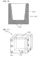
- Fig. 16 is a cross-sectional view of a conventional mold 121 formed of silicon dioxide (SiO 2 ) such as quartz or molten silica, graphite, or the like and having a bottom surface and side surfaces integrally formed therein.
- a mold release material 122 is applied to an inner surface of the mold 121.
- Such a integral-type mold 121 cannot be reused because the mold must be destroyed so as to take out a silicon ingot, so that the production cost of the silicon ingot is significantly high.
- an inner surface of the mold requires a draft angle (taper) for removing a molded object from a metal mold so as to form a raw material into a mold shape by cast molding, press molding, or the like. Therefore, a side surface of the silicon ingot cast by the mold 121 is provided with a reversed taper 123 that spreads toward the head of the ingot from the bottom thereof, so that an end material portion, which will not be a product, is enlarged. Therefore, a high-cost silicon raw material must be removed extra, so that the production cost of the silicon ingot is increased.
- Fig. 17 is a perspective view of a conventional assembly-type mold 131 composed of graphite or the like.
- One bottom surface member 132 and four lateral surface members 133 are joined to each other by driving an assembling screw 134. This allows a silicon ingot to be taken out without destroying the mold 131 differently from the integral-type mold.
- the mold made of high-purity graphite is high in cost, it must be repeatedly used so as to realize the cost reduction of a polycrystalline silicon ingot.
- silicon is a material that solidifies and expands because of a higher density in liquid silicon than in solid silicon
- the bottom surface member 132 and the lateral surface member 133 in the mold experience stress in the direction in which they spread outward.
- the assembly-type mold using the assembling screw 134 the stress due to solidification and expansion at the time of cooling and setting of the silicon melt causes shear stress and tensile stress to be applied to a screwed portion of the mold 131, so that the screw 134 fractures, or a thread of the screw 134 is stripped, for example.
- joining between the bottom surface member 132 and the lateral surface member 133 is loosened, so that the silicon melt leaks out of the mold, or it becomes impossible to reuse the screw 134 and a mold member.
- Such an assembly-type mold using a screw also has a problem that the screw 134 must be attached or detached one at a time in the case of assembling and disassembling, so that it takes much time to perform the work. Further, the bottom surface member 132 and the lateral surface member 133 must be respectively provided with screwed portions, so that the thickness of mold member cannot be reduced. Therefore, the cost of the mold member cannot be reduced, and the production cost of the silicon ingot is increased.
- the mold according to the present invention is set forth in claim 1 and is formed by combing a bottom surface member and a plurality of lateral surface members abutted against the bottom surface member, in which an engaging structure for fixing the adjacent lateral surface members to each other is provided on a side of each of the lateral surface members.
- the mold having such a configuration need not be provided with a screw hole for attaching a screw to the lateral surface member in the mold, the problem that a thread of the screw is stripped, a mold member itself cannot be employed, and the life of a high-cost graphite mold member is shortened is solved. Consequently, the increase in the production cost of a silicon ingot can be restrained. Assembly and disassembly work of the mold is more dramatically simplified, and working efficiency is more significantly improved, as compared with those in a conventional mold to which a large number of screws or bolts had to be attached for the purpose of fixing.
- the engaging structure is a structure in which the projection of one of the lateral surface member and the recess of the other lateral surface member adjacent thereto are engaged with each other, and out of engaging surfaces that are substantially level with a bottom surface of the bottom surface member, a distance between the engaging surface closest to the upper side of the lateral surface member and the upper side is in a range of not less than 1 cm nor more than 8 cm. The setting in this range effectively restrains warping at the top of the lateral surface member, so that the lateral surface member can be kept substantially perpendicular to the bottom surface member.
- the shapes of the engaging structures respectively provided on the sides on both sides of each of the lateral surface members are in an asymmetrical relationship with a center line of the lateral surface member used as a basis, so that the engaging strength between the lateral surface members is increased, so that the effect of warping and deflection is alleviated.
- the top and the bottom of the lateral surface member can be reversed. As a result, the life of the mold member can be lengthened. Since all the shapes of the four lateral surface members are the same, the mold is assembled only by the lateral surface members in one type of shape, so that the production cost of the silicon ingot can be restrained.
- the bottom surface member has a closed groove for dividing its upper surface into a square bottom surface center and a square bottom surface outer periphery, and the respective bottom sides of the four lateral surface members are engaged with the groove of the bottom surface member so as to surround the bottom surface center with the four lateral surface members combined.
- the mold can be so configured that wedge members are respectively arranged in clearances between outer peripheral surfaces of the four lateral surface members engaged with the groove of the bottom surface member and the bottom surface outer periphery.
- the lateral surface members in the mold are pressed by the wedge member, so that a joining portion between the bottom surface member and each of the lateral surface members is firmly fixed at the bottom of the mold to which stress due to the weight of a silicon melt is greatly applied. Therefore, the silicon melt can be prevented from leaking out of the mold, which makes it possible to increase the size of the mold.
- the mold may have a configuration in which the bottom surface member is in a square shape, and the four lateral surface members are abutted against a side surface of the bottom surface member, and comprising a mold holder for placing the bottom surface member and the four lateral surface members that are combined, a plurality of wedge receivers arranged on an upper surface of the mold holder, and wedge members respectively arranged in clearances between the outer peripheral surfaces of the four lateral surface members provided upright so as to surround the bottom surface member and the plurality of wedge receivers.
- the lateral surface members in the mold are pressed by the wedge member, so that a joining portion between the bottom surface member and each of the lateral surface members is firmly fixed at the bottom of the mold to which stress due to the weight of a silicon melt is greatly applied. Therefore, the silicon melt can be prevented from leaking out of the mold, which makes it possible to increase the size of the mold.
- the wedge receiver Even if the wedge receiver is removable from the upper surface of the mold holder, only the wedge receiver can be independently replaced even when it wears with repetitive use, so that the mold holder need not be replaced, and can be continuously reused. Therefore, the cost of the mold can be reduced.
- the joining portion between the bottom surface member and each of the lateral surface members can be firmly fixed by adjusting the clearance between the opposed two wedge receivers even when the joining portion between the bottom surface member and the lateral surface member or a surface where the wedge and the wedge receiver are brought into contact with each other wears.
- a frame-shaped member surrounding the outer periphery of the four lateral surface members integrated by engaging the adjacent lateral surface members for constraining displacement between the lateral surface members.
- the fixing strength of the engaging structure between the lateral surface members is increased by using the frame-shaped member, so that the mold can be increased in size and thinned. Further, even if stress applied to the lateral surface members is large, the lateral surface member can be prevented from warping.
- a frame-shaped member arranged with play given between the frame-shaped member and the four lateral surface members, and pressing jigs may be respectively driven into clearances between the frame-shaped member and four outer corners formed by the adjacent lateral surface members.
- the pressing jig allows the lateral surface member to be firmly pressed even if stress applied to the lateral surface member is large and can prevent the lateral surface member from being deflected. Assembly and disassembly work of the mold is dramatically simplified, and working efficiency is significantly improved.
- the pressing jig may have two jig surfaces respectively abutted against the outer peripheral surfaces of the two lateral surface members forming the outer corner of the mold.
- the pressing jigs may be arranged in four areas of the outer corners of the mold only, so that the number of members can be reduced, leading to simplified work and reduced material costs.
- the outer peripheral surfaces of the two lateral surface members forming the outer corner can be fixed with an uniform force by the two jig surfaces of the pressing jig.
- the pressing jig has a relief groove provided in an area corresponding to the outer corner of the mold such that the outer corner is not directly abutted thereagainst.
- the area corresponding to the outer corner is provided with the relief groove, so that the outer corner of the mold is prevented from being brought into contact with the pressing jig in attaching and detaching the pressing jig to and from the frame-shaped member. Even if attachment and detachment work is repeatedly performed, therefore, the outer corner can be prevented from being deformed and damaged, leading to reduction in the cost of the mold.
- the frame-shaped member may have a projection abutted against the opposed lateral surface member for constraining displacement therebetween provided in its inner periphery.
- the frame-shaped members are respectively arranged at positions of the engaging surfaces. This can prevent the lateral surface member from being deflected even if stress is greatly applied to the lateral surface member as the frame-shaped member is fixed.
- the mold further comprises a mold release material applied to a mold inner surface comprising the bottom surface member and the lateral surface members, and four corners and eight ridges respectively serving as locking sections between the bottom surface member and the lateral surface members and locking sections between the lateral surface members, an inner wall of the mold and the silicon ingot are hardly welded after the silicon melt is solidified, so that the bottom surface member and the lateral surface members can be repeatedly used many times. Since the four corners and the eight ridges respectively serving as the locking sections are reliably sealed by the mold release material, the leakage of the silicon melt is reduced.
- a method of forming a mold according to the present invention is set forth in claim 17 and comprises a first step of applying a mold release material to respective surfaces of one bottom surface member and four lateral surface members, followed by drying; a second step of providing the four lateral surface members upright with the bottom surface member used as a bottom surface, and assembling the members in a box shape such that the surfaces to which the mold release material is applied positioned inside; and a third step of additionally applying the mold release material to locking sections comprising four corners and eight ridges that are formed by the bottom surface member and the lateral surface members.
- Each of the release members may be coated with the mold release material before the mold is assembled, and the mold release material may be only additionally applied only to the joining portion between the mold members after the mold members are assembled to the shape of the mold 1, so that work is dramatically simplified and working efficiency is significantly improved.
- a polycrystalline silicon substrate producing method is a method of producing a silicon ingot using the mold according to the present invention that has been described and obtaining a polycrystalline silicon substrate from the silicon ingot.
- the polycrystalline silicon substrate produced by this method resists repetitive use, and is obtained from the silicon ingot produced using the mold whose assembly and disassembly work is significantly simple, so that lower costs can be expected.
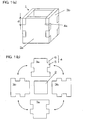
- Fig. 1 (a) is a perspective view showing a mold
- Fig. 1(b) is a developed view thereof.
- reference numeral 1 denotes a mold
- reference numeral 2 denotes a bottom surface member
- reference numeral 3 (3a, 3b) denotes a lateral surface member
- reference numeral 4 denotes an engaging section
- reference numeral 5 denotes a projection
- reference numeral 6 denotes a recess.
- the mold 1 is a division mold that can be divided and assembled.
- the mold 1 is composed of graphite, for example, and is a combination of one bottom surface member 2 composing the bottom of the mold and four lateral surface members 3 (3a and 3b) composing the sides of the mold 1.
- the four lateral surface members 3 are provided so as to surround the outer periphery of the bottom surface member 2 provided at the bottom.
- Each of the lateral surface members 3 comprises an engaging section 4 for engaging the projection 5 and the recess 6 on the side of the lateral surface member 3 so as to couple the lateral surface members 3 to each other.
- the lateral surface members 3 are combined and provided upright by engaging the projection 5 of the one lateral surface member 3a into the recess 6 of the other lateral surface member 3b or engaging the recess 6 of the one lateral surface member 3a into the projection 5 of the other lateral surface member 3b, thereby forming the mold 1.
- the above-mentioned mold 1 has a configuration using no screws, bolts, or the like for assembling and fixing the mold, unlike the conventional mold.
- the density of liquid silicon is higher than that of solid silicon, and silicon is a material that expands when it is solidified. Therefore, silicon experiences stress in the direction in which the bottom surface member 2 and the lateral surface members 3 in the mold 1 spread outward when a silicon melt is cooled and set within the mold 1.
- the mold 1does not have the problem that the fixing of a joining portion between the bottom surface member 2 and the lateral surface member 3 in the mold 1 or between the lateral surface members 3 is loosened by the fracture of a screw, a bolt, or the like and the wear of a thread, as compared with a configuration using screws, bolts, or the like, which can prevent the silicon melt that is being cooled and set within the mold 1 from leaking.
- the mold 1 is so configured that out of engaging surfaces 4a that are surfaces where the projection of the lateral surface member 3 and the recess of the other lateral surface member 3 adjacent thereto are fitted into or engaged with and abutted against each other (refer to surfaces substantially level with the bottom surface of the bottom surface member 2 out of surfaces composing the engaging section 4), the distance d between the engaging surface closest to the upper side of the lateral surface member and the upper side is within a range of not less than 1 cm nor more than 8, as shown in Fig. 1 .
- the distance d is preferably in a range of not less than 1 cm nor more than 4 cm.
- the lateral surface member 3a having the recess 6 is easily moved in a direction indicated by an arrow P both inward and outward because its upper part is not regulated by the other lateral surface member 3b in a joining portion between the projection 5 and the recess 6 respectively positioned at uppermost parts of the lateral surface members 3.
- the movement of the lateral surface member 3b is regulated by the adjacent lateral surface member 3a in a case where its upper part attempts to be curved inward, while there is nothing to be regulated in a case where the upper part attempts to be curved outward.
- the lateral surface member 3 may warp outward due to stress created by cooling and setting of the silicon melt.
- the lateral surface member 3 itself is opened by such warping of the lateral surface member 3, a side surface of a silicon ingot cast by the mold is also inclined, and an end material portion, which will not be a product, of the silicon ingot is enlarged so that an extra high-cost silicon raw material must be removed extra. Therefore, the production cost of the silicon ingot rises.
- the width d from the upper side of the lateral surface member 3 to the engaging surface 4a is as narrow as not less than 1 cm nor more than 8 cm and preferably not less than 1 cm nor more than 4 cm, therefore, warping of the upper part of the lateral surface member 3 caused by stress created by cooling and solidification of the silicon melt can be reduced.
- the range d When the range d is made smaller than 1 cm, wear due to repetitive use particularly extends to the projection 5, so that the projection 5 is liable to be damaged. Therefore, the life of the mold member is shortened.
- the range d is made larger than 8 cm, the upper part of the lateral surface member 3 warps, so that the lateral surface member 3 is not kept substantially perpendicular to the bottom surface member 2, and the end material portion, which will not be a product, is enlarged. Therefore, the production cost of the silicon ingot is increased.
- Fig. 3 (a) is a perspective view showing a mold according to the present invention, and Fig. 3 (b) is developed view thereof.
- a lateral surface member 3c is so adapted that the positions of a projection 5 and a recess 6 in an engaging section 4 that are respectively provided on the sides on both sides thereof are in an asymmetrical relationship with respect to a center line F of the lateral surface member 3c.
- the number of projections 5 and the number of recesses 6 that are provided on the one side of the lateral surface member 3c are respectively even numbers (two each in the drawing).
- the projection 5 and the recess 6 are thus respectively provided at both ends of the lateral surface member 3c so as to have an asymmetrical relationship so that the assembled mold 1 is firmly fixed with the effect of warping and deflection of the lateral surface member 3c alleviated.
- the lateral surface member 3c in the mold 1 according to the present embodiment has the projection 5 and the recess 6 provided on the sides on both sides thereof so as to satisfy a point-symmetrical relationship with respect to a center point G of the lateral surface member 3c.
- the projection 5 and the recess 6 provided on the sides on both sides thereof so as to satisfy a point-symmetrical relationship with respect to a center point G of the lateral surface member 3c.
- the projection 5 and the recess 6 thus have a point-symmetrical structure so that they have the same shape even if they are rotated through 180 degrees. Therefore, the concept on verticality of the lateral surface member 3c is eliminated.
- the mold 1 has a mold heating means composed of a resistance heating heater, an induction heating coil, or the like provided in its upper part, a side wall of the mold 1 being covered with a mold insulating material composed of a graphite molded member or the like, and has a cooling means provided in its lower part.
- a silicon melt poured into the mold 1 is cooled from the bottom of the mold so that the silicon melt can be solidified in one direction upward from the bottom only by being heated from the top of the mold. Therefore, as the upper part of the mold is heated by the mold heating means, the mold member vigorously wears, so that the life of the mold is shortened.
- the lateral surface member has the same shape even if it is rotated through 180 degrees. Therefore, the upper part and the lower part of the lateral surface member can be reversed. As a result, the life of the mold member can be lengthened.
- the distance d from the upper side of the lateral surface member 3 to the engaging surface 4a is made as narrow as not less than 1 cm nor more than 8 cm and preferably not less than 1 cm nor more than 4 cm, warping in the upper part of the lateral surface member 3c caused by stress created when the silicon melt is cooled and solidified can be reduced.
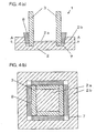
- Fig. 4 (a) is a side sectional view showing a mold according to the present invention
- Fig. 4 (b) is a cross-sectional view taken along a line A - A shown in Fig. 4 (a) .
- a lateral surface member 3 in a mold 1 has an engaging structure described in Figs. 1 to 3 .
- a bottom surface member 2 in the mold 1 has a groove 7 for accepting the bottom side of the assembled lateral surface member 3 on its surface.
- the groove 7 is in a square shape as viewed from the top, and divides the bottom surface member 2 into a bottom surface center 2a and a bottom surface outer periphery 2b.
- the bottom surface center 2a has its sides each corresponding to the bottom side of the lateral surface member 3 and serves as an inner bottom surface of the mold 1.
- wedges 8 are respectively arranged in clearances between outer peripheral surfaces of the four lateral surface members 3 and the bottom surface outer periphery 2b.
- the mold 1 is assembled by providing the bottom surface member 2 with the groove 7, placing the lateral surface member 3 in the groove 7, and driving the wedge 8.
- a carbon fiber-reinforced carbon material (C/C material), for example.
- the shape of the wedge 8 and the number of wedges to be used are not particularly limited.
- one long wedge 8 extending over the whole side surface of the lateral surface member 3 may be driven therein.
- a plurality of small wedges 8 may be attached to the lateral surface member 3.
- the bottom surface center 2a serving as the inner bottom surface of the mold 1 and the bottom surface outer periphery 2b having a wedge receiving function need not have the same height. It is preferable.that the bottom surface outer periphery 2b is made higher than the bottom surface center 2a, as shown in Fig. 4 (a) , for example, because the respective functions can be suitably performed.
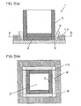
- Fig. 5 (a) is a side sectional view showing another embodiment of a mold according to the present invention
- Fig. 5 (b) is a cross-sectional view taken along a line B - B shown in Fig. 5 (a) .
- a lateral surface member 3 in the mold 1 has the engaging structure described in Figs. 1 to 3 .
- a bottom surface member 2 is in a substantially square shape as viewed from the top, whose sides respectively correspond to the bottom sides of four lateral surface members 3
- the mold 1 further comprises a mold holder 9 for placing a bottom surface member 2, four lateral surface members 3 provided upright so as to surround the bottom surface member 2 on an upper surface of the mold holder 9, a plurality of wedge receivers 10 surrounding respective outer peripheral surfaces of the lateral surface members 3, and wedges 8 respectively arranged in clearances between the outer peripheral surfaces of the lateral surface members 3 and the plurality of wedge receivers 10.
- the mold 1 is assembled by placing the bottom surface member 2 on the mold holder 9 provided with the wedge receivers 10, arranging the four lateral surface members 3 so as to surround the outer periphery of the bottom surface member 2, and respectively driving the wedges 8 between the outer surfaces of the lateral surface members 3 and the wedge receivers 10.
- the wedge receiver 10 and each of the lateral surface members 3 can be firmly fixed to each other without loosening a joining portion between the bottom surface member 2 and the lateral surface member 3 by driving the wedge 8 between the wedge receiver 10 and the lateral surface member 3. Therefore, the leakage of a silicon melt is restrained, so that the size of the mold 1 can be increased.
- the necessity of subjecting the bottom surface member 2 composed of a high-cost graphite mold member to special processing for preventing the leakage of the silicon melt is eliminated, so that the rise in the cost of the mold can be restrained.
- the mold according to the present invention may be so configured that a plurality of wedge receivers 10 (10a, 10b) provided on a mold holder 9 are removable from an upper surface of the mold holder 9, as shown in Fig. 6 . Even in a case where the wedge receiver 10 wears with repetitive use by removably attaching the wedge receiver 10 to the upper surface of the mold holder 9, only the wedge receiver 10 can be independently replaced, and the mold holder 9 need not be replaced and is continuously reusable. Therefore, the cost of the mold can be reduced.
- an example of a method of fixing the wedge receiver 10 is a method of subjecting the mold holder 9 and the wedge receiver 10 to hole processing and engaging a wedge receiver fixing member 11 having such a diameter that it is just engaged with a hole to fix the wedge receiver 10, as shown in Fig. 6 .
- wedge receivers 10 arranged parallel to each of lateral surface members 3 in a mold 1 are fixed so as to be interposed using a wedge receiver fixing bolt 12 and upper and lower nuts 13a and 13b in one or a plurality of areas, as shown in an enlarged sectional view around a wedge shown in Fig. 7 .
- the configuration as shown in Fig. 7 causes the wedge receiver 10 to be fixed to a mold holder 9 more reliably.
- a joining portion between a bottom surface member 2 and each of the lateral surface members 3 can be more firmly fixed to each other.
- the inside dimension D of a wedge receiver fixing hole 14 provided in the mold holder 9 so as to attach the wedge receiver fixing bolt 12 may be made larger than the outside dimension E of the wedge receiver fixing bolt 12, as shown in Fig. 7 . This allows the position of the wedge receiver 10 to be adjusted in a range determined from the inside dimension D and the outside dimension E. Therefore, a clearance between the opposed two wedge receivers can be adjusted.
- the wedge receivers 10a and 10b can be fixed without loosening the fixing of a mold member by adjusting the clearance between the opposed two wedge receivers 10a and 10b even when a joining portion between the bottom surface member 2 and each of the lateral surface members 3 or a surface where the wedge 8 and the wedge receiver 10 are brought into contact with each other wears, for example. It is desirable that the inside dimension D of the wedge receiver fixing hole 14 is increased within 5 mm which is larger than the outside dimension E of the wedge receiver fixing bolt 12.
- the adjustment width of the clearance between the opposed two wedge receivers 10a and 10b is increased by not less than an adjustment amount required to eliminate play produced by the wear of the member, which is not preferable because it becomes difficult to position of the wedge receivers 10a and 10b.
- Fig. 8 (a) is a perspective view showing a mold according to the present invention
- Figs. 8 (b) and 8 (c) are plan views each showing still another embodiment.
- the mold 1 comprises a frame-shaped member 15 arranged so as to surround the outer periphery of its side surfaces integrated by engaging adjacent lateral surface members 3 for constraining displacement therebetween.
- the engaging strength between the lateral surface members 3 is increased, and a joining portion between the bottom surface member 2 and each of the lateral surface members 3 is fixed, so that the mold can be increased in size and thinned. Since the use of the frame-shaped member 15 makes attachment and detachment to and from the mold 1 easy, and allows assembly and disassembly work of the mold 1 to be smoothly performed.
- the frame-shaped member 15 may be in such a shape that the whole periphery of the lateral surface member 3 is fixed, as shown in Fig. 8 (b) , or in such a shape that only the corners of the mold are fixed, as shown in Fig. 8 (c) .
- the frame-shaped member 15 is composed of a carbon fiber-reinforced carbon material (C/C material) being lightweight and high in strength, for example, as in the foregoing. If the thickness h thereof is set to 3 to 10 mm, handling is easy and sufficient strength is obtained.
- C/C material carbon fiber-reinforced carbon material
- the lateral surface member 3 in the mold 1 easily spreads toward its upper end due to expansion caused by cooling and setting of a silicon melt. Particularly when the mold 1 is increased in size and thinned, the effect thereof is great. Therefore, it is preferable that the frame-shaped member 15 is provided within 4 cm from the upper end of the mold 1.
- a mold described below, has a configuration in which play is given between the mold 1 and a frame-shaped member 15, and a pressing jig 16 is arranged in a clearance therebetween, to constrain displacement between lateral surface members 3.
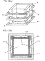
- Figs. 9 , 11 , and 12 are diagrams showing a mold having this configuration, where Fig. 9 (a) is a perspective view showing the configuration of the mold, and Fig. 9 (b) is a plan view thereof.
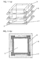
- Fig. 11 (a) is a perspective view showing a mold having another configuration, and Fig. 11 (b) is a plan view thereof.
- Fig. 12 (a) is a perspective view showing a mold having still another configuration, and Fig. 12 (b) is a plan view thereof.
- Figs. 10 (a) to 10 (c) are perspective views showing an example of a pressing jig in the mold according to the present invention shown in Figs. 11 (a) and 11 (b) .
- the mold 1 shown in Fig. 9 comprises a frame-shaped member 15 arranged with play given between the frame-shaped member and the mold 1 so as to surround the outer periphery of four lateral surface members 3 integrated by engaging the adjacent lateral surface members 3.
- a pressing jig 16 is arranged in a clearance between an outer corner formed by the adjacent lateral surface members 3 in the mold 1 and the frame-shaped member 15, to constrain displacement between the lateral surface members 3.
- two pressing jigs 16 are provided in four areas at each of the outer corners per one frame-shaped member 15.
- the two lateral surface members 3 forming the corner of the mold 1 are respectively pressed by the two pressing jigs 16.
- the frame-shaped member 15 is thus arranged with play between the frame-shaped member and the lateral surface member 3 in the mold 1, so that attachment to the mold 1 is easy, and the mold 1 and the frame-shaped member 15 are reliably fixed to each other by the pressing jigs 16. Even when the lateral surface member 3 is thinned, therefore, the mold 1 can be prevented from spreading outward due to expansion caused by cooling and setting of a silicon melt.
- the frame-shaped member 15 can be easily removed from the mold 1 by removing the pressing jigs 16. Therefore, assembly and disassembly work of the mold 1 can be more smoothly performed, as compared with assembly and disassembly work of the conventional mold to which a large number of screws or bolts must be attached for the purpose of fixing.
- the pressing jig 16 is in a wedge shape.
- the thinner pressing jig is inserted into a clearance between the mold 1 and the frame-shaped member 15 and is driven and fixed, so that each of the lateral surface members 3 in the mold 1 can be held more reliably. Further, the fixing strength of the frame-shaped member 15 can be also adjusted by adjusting the driving strength of the pressing jig 16.
- the pressing jig is formed from one member or formed by integrally assembling a plurality of members, as shown in Figs. 10 (a) to 10 (c) .
- the pressing jig may have two jig surfaces respectively abutted against the outer peripheral surfaces of the two lateral surface members 3 forming the outer corner of the mold 1.
- a pressing jig 17 shown in Fig. 10 (a) is an integral-type jig comprising two jig surfaces 17a and 17b.
- the pressing jig 17 is arranged at each of outer corners in four areas on side surfaces of the mold 1 and is so configured that the jig surfaces 17a and 17b are respectively abutted against the outer peripheral surfaces of the two lateral surface members 3 forming the corner. Consequently, the corner between the side surfaces of the mold 1 is held by the one pressing jig 17, so that two surfaces of the lateral surface members 3 forming the corner can be pressed with a more uniform force.
- a pressing jig 18 has a relief groove 18a provided in an area corresponding to an outer corner of the mold 1 such that the outer corner is not directly abutted against the pressing jig 18.
- This can prevent the corner between the side surfaces of the mold 1 from being brought into direct contact with the pressing jig 18 in attaching and detaching the pressing jig 18 to and from the frame-shaped member 15. Even if attachment and detachment work is repeatedly performed, therefore, the corner between the side surfaces of the mold 1 that is easy to damage can be prevented from being deformed and damaged, leading to reduction in the cost of the mold 1.
- a wide portion 19a that is wide in an upper part of an integral-type pressing jig 19.
- the wide portion 19a can be directly pressed in a case where the pressing jig 19 is inserted into a clearance between the mold 1 and a frame-shaped member 7.
- the wide portion 19a may be tapped.
- the pressing jig 19 has such an effect that it can be pulled out with the wide portion 19a held when it is removed, resulting in further improved workability.
- the inner periphery of a frame-shaped member 15 may be provided with projections 15a, directed toward opposed four lateral surface members 3 in the mold 1.
- the lateral surface member 3 in the mold 1 is deflected outward due to expansion caused by cooling and setting of a silicon melt, when a member of the mold 1 is thinned, the effect thereof is increased.
- the frame-shaped member 15 is provided with the projection 15a, an outer peripheral surface of the lateral surface member 3 is abutted against the projection 15a, and the movement thereof is regulated, so that outward deflection of the lateral surface member 3 can be restrained
- the projection amount of the projection 15a may be also the same as the width of a clearance between the mold 1 and the frame-shaped member 15, as also shown in a plan view of Fig. 12 (b) . It is desirable that the projection 15a presses a substantially central portion on an outer peripheral surface of the lateral surface member 3. The reason for this is that the displacement particularly at the center H of the lateral surface member 3 becomes significant due to expansion caused by cooling and setting of the silicon melt.
- projections 15a may be respectively provided in a plurality of (two or three or more) frame-shaped members 15 and brought into contact with one of the lateral surface members 3 in a plurality of areas.
- a straight line formed by connecting projections 15a respectively provided in the upper and lower frame-shaped members 15 passes through the center H.
- the center H is included inside a figure formed by connecting projections 15a respectively provided in the three frame-shaped members 15. The reason for this is that the displacement at the center H can be effectively restrained by each of the projections 15a.
- the projection 15a in the one frame-shaped member 15 may be brought into contact with the one lateral surface member 3 in two or more areas.
- the pressing jigs 16 to 19 are composed of a carbon fiber-reinforced carbon material (C/C material) or the like being lightweight and high in strength. It is desirable that a surface, in contact with the outer peripheral surface of the lateral surface member 3 in the mold 1, of each of the pressing jigs 16 to 19 is a plane, and a surface, in contact with the frame-shaped member 15, of the pressing jig is in a wedge shape having a predetermined slope.
- C/C material carbon fiber-reinforced carbon material
- the lateral surface member 3 in the mold 1 more easily spreads toward its upper end in the configuration according to the present invention due to expansion caused by cooling and setting of the silicon melt. Particularly when the mold 1 is increased in size and thinned, the effect thereof is large. Therefore, it is preferable that the frame-shaped member 15 is provided within 4 cm from the upper end of the mold 1.
- the frame-shaped member 15 is arranged at a position of an engaging surface 4a serving as a surface where a projection of the lateral surface member 3 and a recess of the adjacent lateral surface member 3, which are engaged with each other, are abutted against each other, as shown in Figs. 13 (a) and 13 (b) .
- the engaging surface 4a refers to a surface, which is substantially level with a bottom surface of the bottom surface member 2, out of surfaces composing the engaging section 4. Even if stress is greatly applied to the lateral surface member 3 as the frame-shaped member 15 is fixed, therefore, the lateral surface member 3 can be prevented from being deflected.
- a mold inner surface comprising a bottom surface member 2 and lateral surface members 3 and locking sections comprising four corners and eight ridges are provided with a mold release material.
- the mold release material can be formed by mixing powder of silicon nitride (Si 3 N 4 ) with a PVA (polyvinyl alcohol) solution and applying a mixture obtained to an inner surface of the mold 1, for example.
- Silicon nitride in the form of powder is changed into a slurry form by being mixed with the PVA solution or the like, so that it is easily applied to the mold 1.
- Used as the powder of silicon nitride is one having an average particle diameter of approximately 0.4 to 0.6 ⁇ m.
- Such silicon nitride is changed into a slurry form by being mixed in a polyvinyl alcohol solution having a concentration of approximately 5 to 15 % by weight, and is applied using a paddle, a brush, a dispenser, or the like.
- a mixture of powder of silicon nitride and powder of silicon dioxide may be applied.
- a specific method of forming a mold release material is carried out through three processes, next described.
- a mold release material in the form of a slurry obtained in the above-mentioned way is applied to surfaces of the bottom surface member 2 and the four lateral surface members 3, followed by drying.
- the four lateral surface members 3 are provided upright with the bottom surface member 2 used as a bottom surface, and are assembled in a box shape such that a surface coated with the mold release material positioned inside.
- the mold release material is additionally applied by a dispenser, for example, to locking sections, comprising four corners and eight ridges, which are formed by the bottom surface member 2 and the lateral surface members 3.
- each of the mold members may be coated with the mold release material before the mold 1 is assembled, and the mold release material may be only additionally applied to a joining portion between the mold members, so that work is dramatically simplified and working efficiency is significantly improved.
- the mold according to the present invention can be realized.
- a material for the mold member has been limited to one capable of carrying out an additional process for attaching screws, bolts, or the like to a mold member.
- a graphite material has been used.
- the above-mentioned complicated processing need not be performed, and the structure of the mold member can be significantly simplified. Therefore, the mold member is not limited to the graphite material.
- various types of refractories such as molten silica, silicon nitride, and silicon carbide can be used.
- a monocrystalline silicon ingot may be grown from the silicon melt using monocrystalline silicon held in a predetermined direction at the bottom of the mold as a seed.
- the material is not limited to a semiconductor nonmetal material.
- a metal material may be used, provided that it is cast by a casting method.
- a material mainly composed of carbon for example, a graphite felt and particularly, a mold insulating material (not shown) having its surface subjected to coating processing using carbon powder, or the like may be arranged on the outer periphery of the mold 1.
- the member may be interposed between the wedge 8 and the wedge receiver 10 or between the wedge 8 and the lateral surface member 3.
- the member may be interposed between the frame-shaped member 15 and the lateral surface member 3.
- Such a mold insulating material is for insulating a side surface of the mold 1 to solidify the mold 1 in one direction in a casting method for obtaining a polycrystalline silicon ingot, as described later.
- the polycrystalline silicon substrate is generally produced by a method referred to as a casting method.
- the casting method is a method of cooling and setting a silicon melt within a mold coated with a mold release material to form a polycrystalline silicon ingot. An end of the silicon ingot is removed, the remaining silicon ingot is cut down to desired dimensions, and the cut ingot is sliced to a desired thickness, to obtain a polycrystalline silicon substrate for forming a solar cell.
- a silicon casting device shown in Fig. 14 for example, is used.
- reference numeral 21a denotes a melting crucible
- reference numeral 21b denotes a holding crucible
- reference numeral 22 denotes a pouring port
- reference numeral 1 denotes a mold according to the present invention
- reference numeral 24 denotes heating means
- reference numeral 25 denotes a silicon melt.
- the melting crucible 21a for melting a silicon raw material is held in the holding crucible 21b and arranged therein, and the porting port 22 for pouring the silicon melt by inclining the melting crucible 21a is provided at an upper edge of the melting crucible 21a.
- the heating means 24 is arranged around the melting crucible 21a and the holding crucible 21b, and the mold 1 into which the silicon melt is poured is arranged below the melting crucible 21a and the holding crucible 21b.
- the melting crucible 21a uses high-purity quartz, for example, in consideration of a heat resistance performance, the fact that impurities are not diffused into the silicon melt, and so on.
- the holding crucible 21b is for holding the melting crucible 21a composed of quartz or the like because the melting crucible 21a is softened at high temperatures in the vicinity of a melting point of silicon so that the shape thereof cannot be maintained.
- Used as a material for the holding crucible 21b is graphite or the like.
- the heating means 24 include a resistance heating heater and an induction heating coil.
- the mold 1 arranged below the melting crucible 21a and the holding crucible 21b is used with a mold release material (not shown), described above, applied to its inner part.
- a mold insulating material (not shown) for restraining heat removal is placed around the mold 1.
- a carbon material is generally used for the mold insulating material in consideration of heat resisting properties, heat insulating properties, or the like.
- a cooling plate (not shown) for cooling and setting the poured silicon melt may, in some cases, be placed below the mold 1. These are all arranged within a closed chamber (not shown).
- a method of producing a silicon ingot using the silicon casting device shown in Fig. 14 is as follows. First, a silicon raw material is put into the melting crucible 21a, and the silicon raw material within the melting crucible 21a is dissolved by the heating means 24. After the silicon raw material is completely changed into a melt 25, the melting crucible 21a is inclined to pour the silicon melt into the mold placed below the melting crucible 21a from the pouring port 22 at the upper edge of the melting crucible 21a. After the silicon melt is poured, silicon within the mold is cooled from the bottom and is solidified in one direction, is then slowly cooled while controlling the temperature thereof to a temperature at which it can be taken out of a furnace, and is finally taken out of the furnace to complete the casting.
- the method is a method referred to as a pouring method for completely dissolving a silicon raw material serving as a melt in the mold 1 and pouring the melt, cooling silicon within the mold from the bottom after the melt is poured to solidify the silicon in one direction.
- a pouring method for completely dissolving a silicon raw material serving as a melt in the mold 1 and pouring the melt, cooling silicon within the mold from the bottom after the melt is poured to solidify the silicon in one direction.
- an in-mold melting method for putting a silicon raw material into the mold 1, dissolving the silicon raw material in the mold 1, and cooling the dissolved silicon from the bottom to solidify the silicon may be employed.
- Fig. 15 is a perspective view for explaining a method of slicing an ingot using a wire saw.
- An end material of a polycrystalline silicon ingot produced by the above-mentioned casting method is cut down to predetermined dimensions, to form a semiconductor ingot 31.
- the semiconductor ingot 31 adheres to a slice base 33 made of glass, a carbon material, or a resin with adhesives such as epoxy adhesives, the semiconductor ingot 31 is cut into a plurality of slices using a wire saw device.
- the semiconductor ingot 31 is made to adhere to a slice base 33, and is cut using one wire 35 composed of a piano wire having a diameter of approximately 100 to 300 ⁇ m, for example, while supplying a cutting fluid having abrasive grains of SiC or the like mixed with oil or water referred to as an abrasive grain slurry from upper several areas.
- Spiral grooves are provided so as to be spaced a predetermined distance apart from one another on a main roller 38.
- the wire 35 is pulled out of a wire supply reel, and is arranged substantially parallel to one another with predetermined spacing by being wound so as to be engaged with a groove on the main roller 38.
- a plurality of wires 35 stretched between the two main rollers 38 are moved to travel at high speed by thus rotating the two main rollers 38.
- a plurality of semiconductor ingots 31 are gradually lowered toward the wires 35 and pressed thereagainst, so that each of semiconductor ingots 31 is cut, to produce a semiconductor substrate having a thickness corresponding to the spacing between the wires 35.
- a large number of semiconductor ingots 31 can be simultaneously cut, and a kerf loss (cutting loss) can be reduced because cutting precision is higher than that in another cutting method using an outer peripheral edge, an inner peripheral edge, or the like, and a wire being employed is thin.
- a polycrystalline silicon substrate produced by this method resists repetitive use, and is obtained from a silicon ingot produced using a mold 1 whose assembly and disassembly work is simple, so that lower costs can be expected.
- one bottom surface member (20 mm in thickness) composed of graphite having a mold release material composed of silicon nitride applied thereto of 2 mm in thickness and four lateral surface members (20 mm in thickness) were assembled in a box shape, and were fixed using 32 assembling screws ( ⁇ 5 mm by 40 mm in length), to obtain a mold (220 mm by 220 mm in inside dimensions by 250 mm in height).
- one bottom plate (20 mm in thickness) composed of graphite having a mold release material composed of silicon nitride applied thereto of 2 mm in thickness and four lateral surface members (20 mm in thickness) were assembled in a box shape on a mold fixing holder, and were fixed using a wedge 8 as shown in Fig. 7 , to obtain a mold (220 mm by 220 mm in inside dimensions by 250 mm in height).
- Casting was repeated ten times by each of the two methods, to compare assembling work times of the mold, the presences or absences of leakage of the silicon melt, and wear conditions of the member.
- the average assembling time of the mold was 15 minutes; the number of times of leakage of the silicon melt was one; the number of times of replacement due to fracture of a mold fixing screw and wear of a thread was 22; the number of times of replacement due to wear of a thread processed in a bottom plate or a side plate was seven; and the number of times of replacement due to embedding of a screw that has fractured in a screw mounting hole processed in the bottom plate and the side plate was four.
- the average assembling time of the mold was four minutes; silicon never leaked; and all the members were in a usable state after ten times of casting.
- one bottom surface member (20 mm in thickness) composed of graphite having a mold release material composed of silicon nitride applied thereto of 2 mm in thickness and four lateral surface members (20 mm in thickness) were assembled in a box shape, and were fixed using 40 assembling screws ( ⁇ 5 mm by 40 mm in length), to obtain a mold (350 mm by 350 mm in inside dimensions by 350 mm in height).
- one bottom plate (10 mm in thickness) composed of graphite having a mold release material composed of silicon nitride applied thereto of 2 mm in thickness and four lateral surface members (2 mm in thickness) were assembled in a box shape on a mold fixing holder, and were fixed using a wedge 8 as shown in Fig. 7 , to obtain a mold (350 mm by 350 mm in inside dimensions by 350 mm in height) .
- a frame-shaped member 15 was placed on an engaging surface 4a of a projection and a recess of the lateral surface member 3, to change the height of the projection or the recess positioned in the uppermost part of the lateral surface member 3, that is, a distance d shown in Fig. 1 in a range from 0.5 to 10 cm.
- the silicon melt did not leak, and replacement of the member was not required.
- the height of the projection or the recess in the uppermost part was 8 cm, replacement was required once due to warping deformation of the mold member.
- the silicon melt did not leak.
- the height of the projection or the recess was 0.5 cm and 10 cm other than the most suitable conditions, replacement was required.
- the number of times of replacement of the member was made smaller, as compared with that in the conventional configuration, so that the effect of the present invention was confirmed.
Landscapes
- Chemical & Material Sciences (AREA)
- Organic Chemistry (AREA)
- Inorganic Chemistry (AREA)
- Engineering & Computer Science (AREA)
- Mechanical Engineering (AREA)
- Crystallography & Structural Chemistry (AREA)
- Materials Engineering (AREA)
- Metallurgy (AREA)
- Silicon Compounds (AREA)
Abstract
Claims (18)
- Moule (1) formé en combinant un élément de surface inférieure (2) et une pluralité d'éléments de surface latérale (3) qui butent contre l'élément de surface inférieure (2), dans lequel une structure d'engagement (4) pour fixer les éléments de surface latérale adjacents (3) l'un à l'autre est prévue sur un côté de chacun des éléments de surface latérale (3), et dans lequel les formes des structures d'engagement (4) prévues respectivement sur les côtés sur les deux côtés de l'élément de surface latérale (3) se trouvent dans une relation asymétrique avec un axe médian (F) de l'élément de surface latérale (3).
- Moule selon la revendication 1, dans lequel la structure d'engagement (4) comprend une saillie (5) et un évidement (6) qui sont prévus sur le côté de chacun des éléments de surface latérale (3).
- Moule selon la revendication 1, dans lequel le nombre d'éléments de surface latérale (3) qui butent contre l'élément de surface inférieure (2) est quatre.
- Moule selon l'une quelconque des revendications 1 à 3, dans lequel la structure d'engagement (4) comprend une ou plusieurs surface(s) d'engagement (4a) qui est (sont) sensiblement à niveau avec une surface inférieure de l'élément de surface inférieure (2), et une distance (d) entre un côté supérieur de l'élément de surface latérale (3) et la surface d'engagement (4a) la plus proche de celui-ci est comprise dans la gamme de pas moins de 1 cm à pas plus de 8 cm.
- Moule selon l'une quelconque des revendications 1 à 4, dans lequel les formes des structures d'engagement (4) prévues sur les côtés sur les deux côtés de l'élément de surface latérale (3) se trouvent dans une relation symétrique ponctuelle avec un point central (G) de l'élément de surface latérale (3).
- Moule selon l'une quelconque des revendications 1 à 5, dans lequel:l'élément de surface inférieure respectif (2a) comprend une rainure fermée (7) pour diviser sa surface supérieure en un centre de surface inférieure (2a) et une périphérie extérieure de surface inférieure (2b);les côtés inférieurs des éléments de surface latérale (3) sont engagés avec la rainure (7) de l'élément de surface inférieure de manière à entourer le centre de surface inférieure (2a) avec les éléments de surface latérale (3) combinés; etdes éléments de cale (8) sont agencés respectivement dans des dégagements entre les surfaces périphériques extérieures des éléments de surface latérale (3) engagés avec la rainure (7) de l'élément de surface inférieure et la périphérie extérieure de surface inférieure (2b).
- Moule selon l'une quelconque des revendications 1 à 5, dans lequel:les éléments de surface latérale (3) butent contre une surface latérale de l'élément de surface inférieure (2); et comprenant:un support de moule (9) pour placer l'élément de surface inférieure (2) et les éléments de surface latérale (3) qui sont combinés;un récepteur de cale (10) qui est agencé sur une surface supérieure du support de moule (9); etdes éléments de cale (8) qui sont agencés respectivement dans des dégagements entre les surfaces périphériques extérieures des éléments de surface latérale (3) prévus verticalement de manière à entourer l'élément de surface inférieure (2) et le récepteur de cale (10).
- Moule selon la revendication 7, dans lequel le récepteur de cale (10) peut être enlevé de la surface supérieure du support de moule (9).
- Moule selon la revendication 7 ou 8, dans lequel il existe une pluralité de récepteurs de cale (10), ainsi qu'un espacement entre un des récepteurs de cale (10a) et un autre récepteur de cale (10b) agencé dans une position opposée à celui-ci avec l'élément de surface inférieure (2) et les éléments de surface latérale (3) qui sont combinés et coincés entre ceux-ci sur la surface supérieure du support de moule (9).
- Moule selon l'une quelconque des revendications 1 à 9, comprenant en outre un élément en forme de cadre (15) qui est agencé de manière à entourer la périphérie extérieure des éléments de surface latérale (3) intégrés en engageant les éléments de surface latérale adjacents (3) afin de restreindre un déplacement entre les éléments de surface latérale (3).
- Moule selon l'une quelconque des revendications 1 à 9, comprenant en outre:un élément en forme de cadre (15) qui est agencé de manière à entourer la périphérie extérieure des éléments de surface latérale (3) intégrés en engageant les éléments de surface latérale adjacents (3) et avec un jeu entre l'élément en forme de cadre (15) et les éléments de surface latérale (3); etdes gabarits de serrage (16; 17; 18; 19) qui sont agencés respectivement dans des dégagements entre l'élément en forme de cadre (15) et des coins extérieurs formés par les éléments de surface latérale adjacents (3) afin de restreindre un déplacement entre les éléments de surface latérale (3).
- Moule selon la revendication 11, dans lequel le gabarit de serrage (17; 18; 19) présente deux surfaces de gabarit (17a, 17b) qui butent respectivement contre les surfaces périphériques extérieures des deux éléments de surface latérale (3) qui forment le coin extérieur du moule (1).
- Moule selon la revendication 12, dans lequel le gabarit de serrage (18) comporte une rainure de dépouille (18a) qui est prévue dans une région qui correspond au coin extérieur du moule (1), de telle sorte que le coin extérieur ne bute pas directement contre celle-ci.
- Moule selon l'une quelconque des revendications 11 à 13, dans lequel l'élément en forme de cadre (15) comporte une saillie (15a) qui bute contre l'élément de surface latérale opposé (3) afin de restreindre un déplacement entre ceux-ci prévu dans sa périphérie intérieure.
- Moule selon l'une quelconque des revendications 10 à 14, dans lequel la structure d'engagement (4) présente une ou plusieurs surface(s) d'engagement (4a) qui est (sont) sensiblement à niveau avec la surface inférieure de l'élément de surface inférieure (2), et les éléments en forme de cadre (15) sont respectivement agencés dans des positions des surfaces d'engagement (4a).
- Moule selon l'une quelconque des revendications 1 à 15, comprenant en outre une matière de démoulage qui est appliquée sur une surface intérieure du moule qui comprend l'élément de surface inférieure et l'élément de surface latérale et sur des sections de verrouillage qui sont formées par l'élément de surface inférieure et les éléments de surface latérale.
- Procédé de formation d'un moule (1) selon l'une quelconque des revendications 1 à 16, dans lequel le moule est formé en combinant un élément de surface inférieure (2) et une pluralité d'éléments de surface latérale (3) qui butent contre l'élément de surface inférieure (2), et dans lequel une structure d'engagement (4) pour fixer les éléments de surface latérale adjacents (3) l'un à l'autre est prévue sur un côté de chacun des éléments de surface latérale (3), et dans lequel les formes des structures d'engagement (4) respectivement prévues sur les côtés sur les deux côtés de l'élément de surface latérale (3) se trouvent dans une relation asymétrique avec un axe médian (F) de l'élément de surface latérale (3), le procédé comprenant:une première étape qui consiste à appliquer une matière de démoulage sur les surfaces respectives de l'élément de surface inférieure (2) et sur la pluralité d'éléments de surface latérale (3), suivie par un séchage;une deuxième étape qui consiste à disposer les éléments de surface latérale (3) verticalement avec l'élément de surface inférieure (2) qui est utilisé comme surface inférieure, et à assembler les éléments sous la forme d'une boîte de telle sorte que les surfaces auxquelles la matière de démoulage est appliquée soient positionnées à l'intérieur; etune troisième étape qui consiste à appliquer en plus la matière de démoulage sur les sections de verrouillage qui sont formées par l'élément de surface inférieure (2) et les éléments de surface latérale (3).
- Procédé de production d'un substrat de silicium poly-cristallin, comprenant les étapes qui consistent à produire un lingot de silicium (31) en utilisant le moule (1) selon l'une quelconque des revendications 1 à 16, et à obtenir un substrat de silicium poly-cristallin à partir du lingot de silicium (31).
Applications Claiming Priority (3)
| Application Number | Priority Date | Filing Date | Title |
|---|---|---|---|
| JP2004021174 | 2004-01-29 | ||
| JP2004096814 | 2004-03-29 | ||
| PCT/JP2005/001545 WO2005073129A1 (fr) | 2004-01-29 | 2005-01-27 | Moule, procede de formation de celui-ci, et procede de production d’un substrat en silicium polycristallin utilisant ce moule |
Publications (3)
| Publication Number | Publication Date |
|---|---|
| EP1717201A1 EP1717201A1 (fr) | 2006-11-02 |
| EP1717201A4 EP1717201A4 (fr) | 2008-11-26 |
| EP1717201B1 true EP1717201B1 (fr) | 2012-03-07 |
Family
ID=34829409
Family Applications (1)
| Application Number | Title | Priority Date | Filing Date |
|---|---|---|---|
| EP05704366A Expired - Lifetime EP1717201B1 (fr) | 2004-01-29 | 2005-01-27 | Moule, procede de formation de celui-ci, et procede de production d'un substrat en silicium polycristallin utilisant ce moule |
Country Status (6)
| Country | Link |
|---|---|
| US (1) | US8221111B2 (fr) |
| EP (1) | EP1717201B1 (fr) |
| JP (1) | JP5198731B2 (fr) |
| KR (1) | KR20070019970A (fr) |
| CN (1) | CN1914119B (fr) |
| WO (1) | WO2005073129A1 (fr) |
Families Citing this family (17)
| Publication number | Priority date | Publication date | Assignee | Title |
|---|---|---|---|---|
| JP4993874B2 (ja) * | 2005-05-06 | 2012-08-08 | 京セラ株式会社 | シリコンインゴット用の鋳型 |
| JP2006335582A (ja) * | 2005-05-31 | 2006-12-14 | Daiichi Kiden:Kk | 結晶シリコン製造装置とその製造方法 |
| EP2038454A1 (fr) * | 2006-06-23 | 2009-03-25 | Rec Scanwafer AS | Procédé et creuset pour la solidification directe de lingots de silicium multicristallin de qualité semi-conducteur |
| JP5286589B2 (ja) | 2008-05-01 | 2013-09-11 | イビデン株式会社 | ルツボ保持部材およびその製造方法 |
| US8859034B2 (en) * | 2009-01-28 | 2014-10-14 | Kyocera Corporation | Ingot mold for silicon ingot and method for making the same |
| EP2711445A1 (fr) * | 2009-07-16 | 2014-03-26 | MEMC Singapore Pte. Ltd. | Lingots de silicium multicristallin à faible concentration en oxygène |
| WO2011067201A1 (fr) * | 2009-12-04 | 2011-06-09 | Solarworld Innovations Gmbh | Dispositif servant à contenir une masse fondue de silicium |
| WO2011143067A2 (fr) * | 2010-05-10 | 2011-11-17 | Americarb, Inc. | Boîte de confinement |
| US20110289736A1 (en) * | 2010-05-25 | 2011-12-01 | High Concrete Group Llc | Method and apparatus for covering an end of a cable extending from a form during the manufacture of molded structural members |
| CN103140443B (zh) * | 2010-10-08 | 2015-10-14 | 吉坤日矿日石金属株式会社 | 硅锭制造用容器 |
| DE102010060742A1 (de) * | 2010-11-23 | 2012-05-24 | Kobra Formen Gmbh | Form zur Herstellung von Betonformsteinen |
| DE102011052016A1 (de) * | 2011-07-21 | 2013-01-24 | Deutsches Zentrum für Luft- und Raumfahrt e.V. | Bausatz für einen Schmelztiegel, Schmelztiegel und Verfahren zur Herstellung eines Schmelztiegels |
| ES2439820B1 (es) * | 2012-07-24 | 2015-01-12 | Games Pico Pao, S.L. | Sistema constructivo tridimensional |
| DE102014102980B4 (de) * | 2014-03-06 | 2017-12-21 | Ald Vacuum Technologies Gmbh | Hybridtiegel zur Kristallisation von Materialien, Verwendung des Hybridtiegels, Verfahren zur Herstellung von kristallinem Material sowie kristallines Produkt |
| CN105711022B (zh) * | 2016-04-01 | 2018-04-27 | 沃卡瑞(天津)贸易有限公司 | 滤料专用模具及滤料模块成型方法 |
| CN110625070A (zh) * | 2019-10-17 | 2019-12-31 | 邳州市政隆建设有限公司 | 一种半自动化铸造模具 |
| CN111618247A (zh) * | 2020-04-22 | 2020-09-04 | 安徽帮德电气有限公司 | 一种铝盒加工成型模具 |
Family Cites Families (60)
| Publication number | Priority date | Publication date | Assignee | Title |
|---|---|---|---|---|
| US1386003A (en) * | 1918-10-08 | 1921-08-02 | Westinghouse Electric & Mfg Co | Mold for micarta tubes, rods, and the like |
| US1512018A (en) * | 1922-09-11 | 1924-10-21 | Pinkney P Frazer | Stripper box |
| US1663450A (en) * | 1924-09-06 | 1928-03-20 | Gathmann Engineering Company | Shrink-head casing for ingot molds |
| US1523203A (en) * | 1924-11-01 | 1925-01-13 | Bloomfield H Howard | Feeder for ingot molds |
| US1572705A (en) * | 1925-09-16 | 1926-02-09 | Bourne Fuller Company | Method of molding shrink-head casings |
| US1572706A (en) * | 1925-09-16 | 1926-02-09 | Bourne Fuller Company | Mold for making shrink-head casings |
| US2056673A (en) * | 1930-12-05 | 1936-10-06 | Simonds Saw & Steel Co | Method of and apparatus for making composite ingots |
| US1952817A (en) * | 1931-10-14 | 1934-03-27 | Daniel Mervyn Simmons | Packing case |
| US2039872A (en) * | 1935-01-02 | 1936-05-05 | American Metal Co Ltd | Stool to support molds for casting metal |
| US2057942A (en) * | 1935-01-29 | 1936-10-20 | Fay Marc Aurele Alfred | Toy construction unit |
| US2086212A (en) * | 1935-04-29 | 1937-07-06 | R A Simpson Mfg Company Inc | Butter mold |
| US2433803A (en) * | 1945-06-22 | 1947-12-30 | Carnegie Illinois Steel Corp | Sectional hot top |
| US2465977A (en) * | 1947-04-03 | 1949-03-29 | Carnegie Illinois Steel Corp | Sectional hot top for large molds |
| US2691242A (en) * | 1951-07-03 | 1954-10-12 | F D Wallace | Interlocking toy building panels and blocks built therefrom |
| US2919045A (en) * | 1955-12-29 | 1959-12-29 | Englander Co Inc | Tote boxes |
| US2914825A (en) * | 1957-01-24 | 1959-12-01 | United States Steel Corp | Slotted hot top |
| US3060533A (en) * | 1959-09-16 | 1962-10-30 | Marburg Edgar | Hot tops with exothermic inserts |
| US3165798A (en) * | 1963-01-08 | 1965-01-19 | Bate Micheal Donald La | Self-supporting consumable hot top |
| US3246828A (en) * | 1963-08-12 | 1966-04-19 | Phillips Petroleum Co | Collapsible cartons |
| US3591212A (en) * | 1967-01-11 | 1971-07-06 | Jeff S Rhyne | Construction for dovetail joint |
| CA954267A (en) * | 1970-07-24 | 1974-09-10 | Rinei Kobori | Process and device for butt jointing and assembling panels of a building |
| US3692201A (en) * | 1970-09-23 | 1972-09-19 | Gerald G Garduna | Modular container panel |
| US3924376A (en) * | 1971-06-25 | 1975-12-09 | Sukeo Tsurumi | Cuboidal structure |
| US3743455A (en) * | 1971-09-30 | 1973-07-03 | Gen Dynamics Corp | Apparatus for diffusion molding |
| US3905740A (en) * | 1973-11-19 | 1975-09-16 | Beatrice Foods Co | Molding apparatus |
| US3898051A (en) * | 1973-12-28 | 1975-08-05 | Crystal Syst | Crystal growing |
| JPS52143176A (en) * | 1976-05-25 | 1977-11-29 | Shiyouzou Kumakaha | Packaging box |
| DE2745247C3 (de) * | 1977-10-07 | 1980-03-13 | Wacker-Chemitronic Gesellschaft Fuer Elektronik-Grundstoffe Mbh, 8263 Burghausen | Verfahren und Vorrichtung zur semikontinuierlichen Herstellung von Siliciumformkörpern |
| US4218418A (en) * | 1978-06-22 | 1980-08-19 | Crystal Systems, Inc. | Processes of casting an ingot and making a silica container |
| FR2500768A1 (fr) | 1981-02-27 | 1982-09-03 | Labo Electronique Physique | Creuset demontable, procede de fabrication, et cellules solaires au silicium ainsi obtenues |
| DE3440317C2 (de) * | 1984-11-05 | 1995-02-23 | Kabelmetal Ag | Verfahren zur Herstellung einer Stranggießkokille mit verschleißfesten Formstücken |
| JPS62108515A (ja) * | 1985-11-06 | 1987-05-19 | Osaka Titanium Seizo Kk | 多結晶シリコン半導体の製造方法および鋳造用鋳型 |
| US5161709A (en) * | 1989-01-30 | 1992-11-10 | World Container Corporation | Hinged collapsible container |
| NZ233510A (en) * | 1989-05-03 | 1993-09-27 | Robert John Duncanson | Panels joined by tongue and recess formation |
| JP2871795B2 (ja) * | 1990-03-13 | 1999-03-17 | 富士重工業株式会社 | 複合材部品成形型 |
| KR920009637A (ko) * | 1990-11-13 | 1992-06-25 | 다카다 쥬우이찌로오 | 에어백장치의 모듈커버의 성형방법 |
| US5490604A (en) * | 1991-07-11 | 1996-02-13 | Shape Plastics Corp. | Composter |
| US5501354A (en) * | 1992-05-26 | 1996-03-26 | Stromberg; Per S. | Collapsible container |
| JPH06144824A (ja) | 1992-09-16 | 1994-05-24 | Kawasaki Steel Corp | 多結晶シリコンの製造方法 |
| US5765707A (en) * | 1993-07-02 | 1998-06-16 | Kenevan; Timothy Paul | Modular shipping container |
| US5361923A (en) * | 1993-09-13 | 1994-11-08 | The Fabri-Form Co. | Stackable and collapsible container |
| WO1995018047A1 (fr) * | 1993-12-30 | 1995-07-06 | Hae Soon Oh | Boite pliante et depliante |
| US6253520B1 (en) * | 1995-11-03 | 2001-07-03 | Edward E. Houk | Interlocking components and assembly system |
| BE1010487A6 (nl) * | 1996-06-11 | 1998-10-06 | Unilin Beheer Bv | Vloerbekleding bestaande uit harde vloerpanelen en werkwijze voor het vervaardigen van dergelijke vloerpanelen. |
| CN1092602C (zh) * | 1996-10-14 | 2002-10-16 | 川崎制铁株式会社 | 多晶硅的制造方法和装置 |
| US6074523A (en) * | 1996-11-11 | 2000-06-13 | Nippon Kodoshi Corporation | Method of manufacturing highly-airtightened porous paper |
| JPH10188285A (ja) | 1996-12-19 | 1998-07-21 | Sony Corp | 光学記録方法及び光学記録媒体 |
| JPH10182285A (ja) | 1996-12-20 | 1998-07-07 | Kawasaki Steel Corp | 金属シリコン凝固精製用鋳型 |
| JPH10190025A (ja) | 1996-12-24 | 1998-07-21 | Kawasaki Steel Corp | 多結晶シリコンインゴット鋳造用鋳型 |
| US5895045A (en) * | 1997-05-27 | 1999-04-20 | Serigraph, Inc. | Modular card construction toy |
| JP3520957B2 (ja) * | 1997-06-23 | 2004-04-19 | シャープ株式会社 | 多結晶半導体インゴットの製造方法および装置 |
| ES2221307T3 (es) * | 1998-01-26 | 2004-12-16 | Pqr 59 Properties (Pty) Ltd. | Recipiente apilable. |
| US6202847B1 (en) * | 1999-01-19 | 2001-03-20 | Design Ideas, Ltd. | Stackable boxes |
| GB9911979D0 (en) * | 1999-05-24 | 1999-07-21 | British Nuclear Fuels Plc | A container for nuclear fuel elements |
| JP3360111B2 (ja) | 1999-07-23 | 2002-12-24 | 独立行政法人産業技術総合研究所 | ヒステリシスが小さく水蒸気耐久性のある吸放湿材料 |
| US6843386B2 (en) * | 2001-01-15 | 2005-01-18 | Norseman Plastics Limited | Biased latch hinge |
| US7159730B2 (en) * | 2002-01-23 | 2007-01-09 | Donald Rumpel | Folding crate with array connection features |
| US8021483B2 (en) * | 2002-02-20 | 2011-09-20 | Hemlock Semiconductor Corporation | Flowable chips and methods for the preparation and use of same, and apparatus for use in the methods |
| PL191233B1 (pl) * | 2002-12-31 | 2006-04-28 | Barlinek Sa | Panel podłogowy |
| US7017766B2 (en) * | 2003-03-10 | 2006-03-28 | Rehrig Pacific Company | Collapsible container with side wall latching capability |
-
2005
- 2005-01-27 EP EP05704366A patent/EP1717201B1/fr not_active Expired - Lifetime
- 2005-01-27 KR KR1020067014475A patent/KR20070019970A/ko not_active Withdrawn
- 2005-01-27 WO PCT/JP2005/001545 patent/WO2005073129A1/fr not_active Ceased
- 2005-01-27 CN CN200580003282XA patent/CN1914119B/zh not_active Expired - Fee Related
- 2005-01-27 JP JP2005517569A patent/JP5198731B2/ja not_active Expired - Fee Related
- 2005-01-27 US US10/597,514 patent/US8221111B2/en not_active Expired - Fee Related
Also Published As
| Publication number | Publication date |
|---|---|
| CN1914119B (zh) | 2010-09-29 |
| EP1717201A1 (fr) | 2006-11-02 |
| KR20070019970A (ko) | 2007-02-16 |
| US8221111B2 (en) | 2012-07-17 |
| JP5198731B2 (ja) | 2013-05-15 |
| CN1914119A (zh) | 2007-02-14 |
| WO2005073129A1 (fr) | 2005-08-11 |
| JPWO2005073129A1 (ja) | 2007-09-13 |
| EP1717201A4 (fr) | 2008-11-26 |
| US20080230678A1 (en) | 2008-09-25 |
Similar Documents
| Publication | Publication Date | Title |
|---|---|---|
| US8221111B2 (en) | Mold, method of forming the same, and method of producing polycrystalline silicon substrate using the mold | |
| US7540919B2 (en) | Solidification of crystalline silicon from reusable crucible molds | |
| CN102337582B (zh) | 制造硅晶铸锭的方法 | |
| KR101281033B1 (ko) | 온도 조절이 용이한 연속주조법을 이용한 태양전지용 실리콘 기판 제조 장치 및 이를 이용한 실리콘 기판 제조 방법 | |
| JP4993874B2 (ja) | シリコンインゴット用の鋳型 | |
| KR101080757B1 (ko) | 연속주조법을 이용한 태양전지용 실리콘 기판 직접 제조 장치, 이를 이용하여 제조된 태양전지용 실리콘 기판 및 그 제조 방법 | |
| CN201942777U (zh) | 一种多晶铸锭炉石墨坩埚组件 | |
| JP3993814B2 (ja) | 多結晶シリコンインゴットの切断方法 | |
| JP4497943B2 (ja) | シリコン鋳造用鋳型とそれを用いたシリコン鋳造装置 | |
| CN106835264A (zh) | 一种籽晶夹持器 | |
| CN103140443B (zh) | 硅锭制造用容器 | |
| JP4675550B2 (ja) | 一方向凝固シリコンインゴット及びこの製造方法並びにシリコン板及び太陽電池用基板 | |
| JPH09263489A (ja) | シリコン鋳造用鋳型および鋳造法 | |
| JP4726454B2 (ja) | 多結晶シリコンインゴットの鋳造方法、これを用いた多結晶シリコンインゴット、多結晶シリコン基板、並びに太陽電池素子 | |
| JP4741341B2 (ja) | 半導体インゴットの切断方法 | |
| JP2006111529A (ja) | シリコン鋳造用鋳型 | |
| CN221936313U (zh) | 一种籽晶磨削工装 | |
| JP2007015010A (ja) | 鋳型 | |
| JP4412919B2 (ja) | 鋳造装置 | |
| JP4365669B2 (ja) | シリコン鋳造用鋳型 | |
| CN112899777A (zh) | 籽晶片及其制备方法、晶硅锭的制备方法 | |
| JP2006272373A (ja) | 鋳型及びこれを用いた鋳造装置並びに多結晶シリコンインゴットの製造方法 | |
| JPH0558781A (ja) | 多結晶シリコン半導体の製造方法 | |
| Schmid et al. | Heat exchanger method, ingot casting; fixed abrasive method, multi-wire slicing: Phase II. Silicon sheet growth development for the Large-Area Silicon Sheet Task of the Low-Cost Silicon Solar Array Project. Quarterly progress report No. 2, January 1, 1978--March 31, 1978 |
Legal Events
| Date | Code | Title | Description |
|---|---|---|---|
| PUAI | Public reference made under article 153(3) epc to a published international application that has entered the european phase |
Free format text: ORIGINAL CODE: 0009012 |
|
| 17P | Request for examination filed |
Effective date: 20060826 |
|
| AK | Designated contracting states |
Kind code of ref document: A1 Designated state(s): DE GB |
|
| RIN1 | Information on inventor provided before grant (corrected) |
Inventor name: AMANO, YOSHIYUKI,C/O KYOCERA CORPORATION Inventor name: SAKAI, YOUHEI,C/O KYOCERA CORPORATION |
|
| DAX | Request for extension of the european patent (deleted) | ||
| RBV | Designated contracting states (corrected) |
Designated state(s): DE GB |
|
| A4 | Supplementary search report drawn up and despatched |
Effective date: 20081023 |
|
| 17Q | First examination report despatched |
Effective date: 20090310 |
|
| REG | Reference to a national code |
Ref country code: DE Ref legal event code: R079 Ref document number: 602005033020 Country of ref document: DE Free format text: PREVIOUS MAIN CLASS: C01B0033020000 Ipc: B22C0009000000 |
|
| RIC1 | Information provided on ipc code assigned before grant |
Ipc: C30B 11/00 20060101ALI20110211BHEP Ipc: C01B 33/02 20060101ALI20110211BHEP Ipc: B22C 9/00 20060101AFI20110211BHEP |
|
| GRAP | Despatch of communication of intention to grant a patent |
Free format text: ORIGINAL CODE: EPIDOSNIGR1 |
|
| GRAS | Grant fee paid |
Free format text: ORIGINAL CODE: EPIDOSNIGR3 |
|
| GRAA | (expected) grant |
Free format text: ORIGINAL CODE: 0009210 |
|
| AK | Designated contracting states |
Kind code of ref document: B1 Designated state(s): DE GB |
|
| REG | Reference to a national code |
Ref country code: GB Ref legal event code: FG4D |
|
| REG | Reference to a national code |
Ref country code: DE Ref legal event code: R096 Ref document number: 602005033020 Country of ref document: DE Effective date: 20120503 |
|
| PLBE | No opposition filed within time limit |
Free format text: ORIGINAL CODE: 0009261 |
|
| STAA | Information on the status of an ep patent application or granted ep patent |
Free format text: STATUS: NO OPPOSITION FILED WITHIN TIME LIMIT |
|
| 26N | No opposition filed |
Effective date: 20121210 |
|
| REG | Reference to a national code |
Ref country code: DE Ref legal event code: R097 Ref document number: 602005033020 Country of ref document: DE Effective date: 20121210 |
|
| REG | Reference to a national code |
Representative=s name: VIERING, JENTSCHURA & PARTNER PATENT- UND RECH, DE Ref country code: DE Ref legal event code: R082 Ref document number: 602005033020 Country of ref document: DE Ref country code: DE Ref legal event code: R082 Ref document number: 602005033020 Country of ref document: DE Representative=s name: VIERING, JENTSCHURA & PARTNER MBB PATENT- UND , DE |
|
| REG | Reference to a national code |
Ref country code: DE Ref legal event code: R082 Ref document number: 602005033020 Country of ref document: DE Representative=s name: VIERING, JENTSCHURA & PARTNER PATENT- UND RECH, DE Ref country code: DE Ref legal event code: R082 Ref document number: 602005033020 Country of ref document: DE Representative=s name: VIERING, JENTSCHURA & PARTNER MBB PATENT- UND , DE |
|
| PGFP | Annual fee paid to national office [announced via postgrant information from national office to epo] |
Ref country code: DE Payment date: 20160119 Year of fee payment: 12 |
|
| PGFP | Annual fee paid to national office [announced via postgrant information from national office to epo] |
Ref country code: GB Payment date: 20160127 Year of fee payment: 12 |
|
| REG | Reference to a national code |
Ref country code: DE Ref legal event code: R119 Ref document number: 602005033020 Country of ref document: DE |
|
| GBPC | Gb: european patent ceased through non-payment of renewal fee |
Effective date: 20170127 |
|
| PG25 | Lapsed in a contracting state [announced via postgrant information from national office to epo] |
Ref country code: DE Free format text: LAPSE BECAUSE OF NON-PAYMENT OF DUE FEES Effective date: 20170801 Ref country code: GB Free format text: LAPSE BECAUSE OF NON-PAYMENT OF DUE FEES Effective date: 20170127 |