EP1717609A1 - Spektraler Reinigungsfilter für einen mehrschichtigen Spiegel, lithografische Vorrichtung mit einem derartigen mehrschichtigen Spiegel, Verfahren zur Vergrößerung des Verhältnisses von erwünschter und unerwünschter Strahlung sowie Geräteherstellungsverfahren - Google Patents
Spektraler Reinigungsfilter für einen mehrschichtigen Spiegel, lithografische Vorrichtung mit einem derartigen mehrschichtigen Spiegel, Verfahren zur Vergrößerung des Verhältnisses von erwünschter und unerwünschter Strahlung sowie Geräteherstellungsverfahren Download PDFInfo
- Publication number
- EP1717609A1 EP1717609A1 EP06113136A EP06113136A EP1717609A1 EP 1717609 A1 EP1717609 A1 EP 1717609A1 EP 06113136 A EP06113136 A EP 06113136A EP 06113136 A EP06113136 A EP 06113136A EP 1717609 A1 EP1717609 A1 EP 1717609A1
- Authority
- EP
- European Patent Office
- Prior art keywords
- layer
- radiation
- mirror
- spectral purity
- thickness
- Prior art date
- Legal status (The legal status is an assumption and is not a legal conclusion. Google has not performed a legal analysis and makes no representation as to the accuracy of the status listed.)
- Granted
Links
Images



Classifications
-
- G—PHYSICS
- G03—PHOTOGRAPHY; CINEMATOGRAPHY; ANALOGOUS TECHNIQUES USING WAVES OTHER THAN OPTICAL WAVES; ELECTROGRAPHY; HOLOGRAPHY
- G03F—PHOTOMECHANICAL PRODUCTION OF TEXTURED OR PATTERNED SURFACES, e.g. FOR PRINTING, FOR PROCESSING OF SEMICONDUCTOR DEVICES; MATERIALS THEREFOR; ORIGINALS THEREFOR; APPARATUS SPECIALLY ADAPTED THEREFOR
- G03F7/00—Photomechanical, e.g. photolithographic, production of textured or patterned surfaces, e.g. printing surfaces; Materials therefor, e.g. comprising photoresists; Apparatus specially adapted therefor
- G03F7/70—Microphotolithographic exposure; Apparatus therefor
- G03F7/70216—Mask projection systems
- G03F7/70308—Optical correction elements, filters or phase plates for manipulating imaging light, e.g. intensity, wavelength, polarisation, phase or image shift
-
- B—PERFORMING OPERATIONS; TRANSPORTING
- B82—NANOTECHNOLOGY
- B82Y—SPECIFIC USES OR APPLICATIONS OF NANOSTRUCTURES; MEASUREMENT OR ANALYSIS OF NANOSTRUCTURES; MANUFACTURE OR TREATMENT OF NANOSTRUCTURES
- B82Y10/00—Nanotechnology for information processing, storage or transmission, e.g. quantum computing or single electron logic
-
- B—PERFORMING OPERATIONS; TRANSPORTING
- B82—NANOTECHNOLOGY
- B82Y—SPECIFIC USES OR APPLICATIONS OF NANOSTRUCTURES; MEASUREMENT OR ANALYSIS OF NANOSTRUCTURES; MANUFACTURE OR TREATMENT OF NANOSTRUCTURES
- B82Y40/00—Manufacture or treatment of nanostructures
-
- G—PHYSICS
- G02—OPTICS
- G02B—OPTICAL ELEMENTS, SYSTEMS OR APPARATUS
- G02B1/00—Optical elements characterised by the material of which they are made; Optical coatings for optical elements
- G02B1/10—Optical coatings produced by application to, or surface treatment of, optical elements
-
- G—PHYSICS
- G02—OPTICS
- G02B—OPTICAL ELEMENTS, SYSTEMS OR APPARATUS
- G02B5/00—Optical elements other than lenses
- G02B5/08—Mirrors
- G02B5/0816—Multilayer mirrors, i.e. having two or more reflecting layers
-
- G—PHYSICS
- G02—OPTICS
- G02B—OPTICAL ELEMENTS, SYSTEMS OR APPARATUS
- G02B5/00—Optical elements other than lenses
- G02B5/08—Mirrors
- G02B5/0891—Ultraviolet [UV] mirrors
-
- G—PHYSICS
- G02—OPTICS
- G02B—OPTICAL ELEMENTS, SYSTEMS OR APPARATUS
- G02B5/00—Optical elements other than lenses
- G02B5/20—Filters
- G02B5/28—Interference filters
- G02B5/283—Interference filters designed for the ultraviolet
-
- G—PHYSICS
- G03—PHOTOGRAPHY; CINEMATOGRAPHY; ANALOGOUS TECHNIQUES USING WAVES OTHER THAN OPTICAL WAVES; ELECTROGRAPHY; HOLOGRAPHY
- G03F—PHOTOMECHANICAL PRODUCTION OF TEXTURED OR PATTERNED SURFACES, e.g. FOR PRINTING, FOR PROCESSING OF SEMICONDUCTOR DEVICES; MATERIALS THEREFOR; ORIGINALS THEREFOR; APPARATUS SPECIALLY ADAPTED THEREFOR
- G03F1/00—Originals for photomechanical production of textured or patterned surfaces, e.g., masks, photo-masks, reticles; Mask blanks or pellicles therefor; Containers specially adapted therefor; Preparation thereof
- G03F1/22—Masks or mask blanks for imaging by radiation of 100nm or shorter wavelength, e.g. X-ray masks, extreme ultraviolet [EUV] masks; Preparation thereof
- G03F1/24—Reflection masks; Preparation thereof
-
- G—PHYSICS
- G03—PHOTOGRAPHY; CINEMATOGRAPHY; ANALOGOUS TECHNIQUES USING WAVES OTHER THAN OPTICAL WAVES; ELECTROGRAPHY; HOLOGRAPHY
- G03F—PHOTOMECHANICAL PRODUCTION OF TEXTURED OR PATTERNED SURFACES, e.g. FOR PRINTING, FOR PROCESSING OF SEMICONDUCTOR DEVICES; MATERIALS THEREFOR; ORIGINALS THEREFOR; APPARATUS SPECIALLY ADAPTED THEREFOR
- G03F7/00—Photomechanical, e.g. photolithographic, production of textured or patterned surfaces, e.g. printing surfaces; Materials therefor, e.g. comprising photoresists; Apparatus specially adapted therefor
- G03F7/70—Microphotolithographic exposure; Apparatus therefor
- G03F7/70008—Production of exposure light, i.e. light sources
- G03F7/70033—Production of exposure light, i.e. light sources by plasma extreme ultraviolet [EUV] sources
-
- G—PHYSICS
- G03—PHOTOGRAPHY; CINEMATOGRAPHY; ANALOGOUS TECHNIQUES USING WAVES OTHER THAN OPTICAL WAVES; ELECTROGRAPHY; HOLOGRAPHY
- G03F—PHOTOMECHANICAL PRODUCTION OF TEXTURED OR PATTERNED SURFACES, e.g. FOR PRINTING, FOR PROCESSING OF SEMICONDUCTOR DEVICES; MATERIALS THEREFOR; ORIGINALS THEREFOR; APPARATUS SPECIALLY ADAPTED THEREFOR
- G03F7/00—Photomechanical, e.g. photolithographic, production of textured or patterned surfaces, e.g. printing surfaces; Materials therefor, e.g. comprising photoresists; Apparatus specially adapted therefor
- G03F7/70—Microphotolithographic exposure; Apparatus therefor
- G03F7/70216—Mask projection systems
- G03F7/70233—Optical aspects of catoptric systems, i.e. comprising only reflective elements, e.g. extreme ultraviolet [EUV] projection systems
-
- G—PHYSICS
- G03—PHOTOGRAPHY; CINEMATOGRAPHY; ANALOGOUS TECHNIQUES USING WAVES OTHER THAN OPTICAL WAVES; ELECTROGRAPHY; HOLOGRAPHY
- G03F—PHOTOMECHANICAL PRODUCTION OF TEXTURED OR PATTERNED SURFACES, e.g. FOR PRINTING, FOR PROCESSING OF SEMICONDUCTOR DEVICES; MATERIALS THEREFOR; ORIGINALS THEREFOR; APPARATUS SPECIALLY ADAPTED THEREFOR
- G03F7/00—Photomechanical, e.g. photolithographic, production of textured or patterned surfaces, e.g. printing surfaces; Materials therefor, e.g. comprising photoresists; Apparatus specially adapted therefor
- G03F7/70—Microphotolithographic exposure; Apparatus therefor
- G03F7/70483—Information management; Active and passive control; Testing; Wafer monitoring, e.g. pattern monitoring
- G03F7/7055—Exposure light control in all parts of the microlithographic apparatus, e.g. pulse length control or light interruption
- G03F7/70575—Wavelength control, e.g. control of bandwidth, multiple wavelength, selection of wavelength or matching of optical components to wavelength
-
- G—PHYSICS
- G03—PHOTOGRAPHY; CINEMATOGRAPHY; ANALOGOUS TECHNIQUES USING WAVES OTHER THAN OPTICAL WAVES; ELECTROGRAPHY; HOLOGRAPHY
- G03F—PHOTOMECHANICAL PRODUCTION OF TEXTURED OR PATTERNED SURFACES, e.g. FOR PRINTING, FOR PROCESSING OF SEMICONDUCTOR DEVICES; MATERIALS THEREFOR; ORIGINALS THEREFOR; APPARATUS SPECIALLY ADAPTED THEREFOR
- G03F7/00—Photomechanical, e.g. photolithographic, production of textured or patterned surfaces, e.g. printing surfaces; Materials therefor, e.g. comprising photoresists; Apparatus specially adapted therefor
- G03F7/70—Microphotolithographic exposure; Apparatus therefor
- G03F7/708—Construction of apparatus, e.g. environment aspects, hygiene aspects or materials
- G03F7/7095—Materials, e.g. materials for housing, stage or other support having particular properties, e.g. weight, strength, conductivity, thermal expansion coefficient
- G03F7/70958—Optical materials or coatings, e.g. with particular transmittance, reflectance or anti-reflection properties
-
- G—PHYSICS
- G21—NUCLEAR PHYSICS; NUCLEAR ENGINEERING
- G21K—HANDLING OF PARTICLES OR IONISING RADIATION NOT OTHERWISE PROVIDED FOR; IRRADIATION DEVICES; GAMMA RAY OR X-RAY MICROSCOPES
- G21K1/00—Arrangements for handling particles or ionising radiation, e.g. focusing or moderating
- G21K1/06—Arrangements for handling particles or ionising radiation, e.g. focusing or moderating using diffraction, refraction or reflection, e.g. monochromators
- G21K1/062—Devices having a multilayer structure
-
- G—PHYSICS
- G21—NUCLEAR PHYSICS; NUCLEAR ENGINEERING
- G21K—HANDLING OF PARTICLES OR IONISING RADIATION NOT OTHERWISE PROVIDED FOR; IRRADIATION DEVICES; GAMMA RAY OR X-RAY MICROSCOPES
- G21K2201/00—Arrangements for handling radiation or particles
- G21K2201/06—Arrangements for handling radiation or particles using diffractive, refractive or reflecting elements
- G21K2201/067—Construction details
Definitions
- the present invention relates to a spectral purity filter for a multi-layer mirror, a lithographic apparatus including such multi-layer mirror, a method for enlarging the ratio of desired radiation and undesired radiation and a device manufacturing method wherein such a multi-layer mirror is used.
- a lithographic apparatus is a machine that applies a desired pattern onto a substrate, usually onto a target portion of the substrate.
- a lithographic apparatus can be used, for example, in the manufacture of integrated circuits (ICs).
- a patterning device which is alternatively referred to as a mask or a reticle, may be used to generate a circuit pattern to be formed on an individual layer of the IC.
- This pattern can be transferred onto a target portion (e.g. including part of, one, or several dies) on a substrate (e.g. a silicon wafer). Transfer of the pattern is typically via imaging onto a layer of radiation-sensitive material (resist) provided on the substrate.
- resist radiation-sensitive material
- a single substrate will contain a network of adjacent target portions that are successively patterned.
- lithographic apparatus include steppers, in which each target portion is irradiated by exposing an entire pattern onto the target portion at one time, and scanners, in which each target portion is irradiated by scanning the pattern through a radiation beam in a given direction (the "scanning" direction) while synchronously scanning the substrate parallel or anti-parallel to this direction. It is also possible to transfer the pattern from the patterning device to the substrate by imprinting the pattern onto the substrate.
- EUV Extreme UtraViolet
- soft x-ray Possible sources include, for example, laser-produced plasma sources, discharge plasma sources, or synchrotron radiation from electron storage rings.
- the source of EUV radiation is typically a plasma source, for example a laser-produced plasma or a discharge source.
- an EUV source may emit several different wavelengths of light, some of which may be undesired radiation, such as deep ultra-violet radiation (DUV).
- DUV deep ultra-violet radiation
- This non-EUV radiation can, in some instances, be harmful for the EUV lithography system because it can result in a loss of contrast.
- SPPF spectral purity filter
- spectral purity filters are based on blazed gratings. These gratings are often difficult to produce, since the surface quality of the triangular shaped pattern should be high. For example, for some gratings the roughness of the surface should be lower than 1 nm RMS.
- the current spectral purity filter folds the path of the light, which means that it cannot be removed from the system unless another mirror is used to replace the spectral purity filter, thereby causing losses. In order to keep flexibility it may be desirable to be able to remove the spectral purity filter from the system at will, in order to evade the losses caused by the spectral purity filter.
- the present invention provides a multi-layer mirror including on top of the multi-layer mirror a spectral purity enhancement layer, especially for application in an EUV lithographic apparatus.
- This spectral purity enhancement layer includes at least a first spectral purity enhancement layer, but between the multi-layer mirror and first spectral purity enhancement layer there may be also an intermediate layer or a second spectral purity enhancement layer and intermediate layer.
- multi-layer mirrors with the following configurations: multi-layer mirror/first spectral purity enhancement layer; multi-layer mirror/intermediate layer/first spectral purity enhancement layer; and multi-layer mirror/second spectral purity enhancement layer/intermediate layer/first spectral purity enhancement layer.
- These and other embodiments may enhance the spectral purity of normal incidence radiation, such that DUV radiation is diminished relatively stronger than EUV radiation.
- FIG. 1 schematically depicts a lithographic apparatus 1 according to an embodiment of the present invention.
- the apparatus 1 includes an illumination system (illuminator) IL configured to condition a radiation beam B (e.g. UV radiation or EUV radiation).
- a support (e.g. a mask table) MT is configured to support a patterning device (e.g. a mask) MA and is connected to a first positioning device PM configured to accurately position the patterning device in accordance with certain parameters.
- a substrate table (e.g. a wafer table) WT is configured to hold a substrate (e.g. a resist-coated wafer) W and is connected to a second positioning device PW configured to accurately position the substrate in accordance with certain parameters.
- a projection system (e.g. a refractive projection lens system) PS is configured to project a pattern imparted to the radiation beam B by patterning device MA onto a target portion C (e.g. including one or more dies) of the substrate W.
- the illumination system may include various types of optical components, such as refractive, reflective, magnetic, electromagnetic, electrostatic or other types of optical components, or any combination thereof, to direct, shape, and/or control radiation.
- optical components such as refractive, reflective, magnetic, electromagnetic, electrostatic or other types of optical components, or any combination thereof, to direct, shape, and/or control radiation.
- the support supports, e.g. bears the weight of, the patterning device. It holds the patterning device in a manner that depends on the orientation of the patterning device, the design of the lithographic apparatus, and other conditions, such as for example whether or not the patterning device is held in a vacuum environment.
- the support can use mechanical, vacuum, electrostatic or other clamping techniques to hold the patterning device.
- the support may be a frame or a table, for example, which may be fixed or movable as required. The support may ensure that the patterning device is at a desired position, for example with respect to the projection system. Any use of the terms "reticle” or “mask” herein may be considered synonymous with the more general term "patterning device.”
- patterning device used herein should be broadly interpreted as referring to any device that can be used to impart a radiation beam with a pattern in its cross-section such as to create a pattern in a target portion of the substrate. It should be noted that the pattern imparted to the radiation beam may not exactly correspond to the desired pattern in the target portion of the substrate, for example if the pattern includes phase-shifting features or so called assist features. Generally, the pattern imparted to the radiation beam will correspond to a particular functional layer in a device being created in the target portion, such as an integrated circuit.
- the patterning device may be transmissive or reflective.
- Examples of patterning devices include masks, programmable mirror arrays, and programmable LCD panels.
- Masks are well known in lithography, and include mask types such as binary, alternating phase-shift, and attenuated phase-shift, as well as various hybrid mask types.
- An example of a programmable mirror array employs a matrix arrangement of small mirrors, each of which can be individually tilted so as to reflect an incoming radiation beam in different directions. The tilted mirrors impart a pattern in a radiation beam which is reflected by the mirror matrix.
- projection system used herein should be broadly interpreted as encompassing any type of projection system, including refractive, reflective, catadioptric, magnetic, electromagnetic and electrostatic optical systems, or any combination thereof, as appropriate for the exposure radiation being used, or for other factors such as the use of an immersion liquid or the use of a vacuum. Any use of the term “projection lens” herein may be considered as synonymous with the more general term “projection system”.
- the apparatus is of a reflective type (e.g. employing a reflective mask).
- the apparatus may be of a transmissive type (e.g. employing a transmissive mask).
- the lithographic apparatus may be of a type having two (dual stage) or more substrate tables (and/or two or more mask tables). In such "multiple stage” machines the additional tables may be used in parallel, or preparatory processes may be carried out on one or more tables while one or more other tables are being used for exposure.
- the lithographic apparatus may also be of a type wherein at least a portion of the substrate may be covered by a liquid having a relatively high refractive index, e.g. water, so as to fill a space between the projection system and the substrate.
- a liquid having a relatively high refractive index e.g. water
- An immersion liquid may also be applied to other spaces in the lithographic apparatus, for example, between the mask and the projection system. Immersion techniques are well known in the art for increasing the numerical aperture of projection systems.
- immersion as used herein does not mean that a structure, such as a substrate, must be submerged in liquid, but rather only means that liquid is located, for example, between the projection system and the substrate during exposure.
- the illuminator IL receives radiation from a radiation source SO.
- the source and the lithographic apparatus may be separate entities, for example when the source is an excimer laser. In such cases, the source is not considered to form part of the lithographic apparatus and the radiation is passed from the source SO to the illuminator IL with the aid of a beam delivery system including, for example, suitable directing mirrors and/or a beam expander. In other cases the source may be an integral part of the lithographic apparatus, for example when the source is a mercury lamp.
- the source SO and the illuminator IL, together with the beam delivery system if required, may be referred to as a radiation system.
- the illuminator IL may include an adjusting device configured to adjust the angular intensity distribution of the radiation beam. Generally, at least the outer and/or inner radial extent (commonly referred to as ⁇ -outer and ⁇ -inner, respectively) of the intensity distribution in a pupil plane of the illuminator can be adjusted.
- the illuminator IL may include various other components, such as an integrator and a condenser. The illuminator may be used to condition the radiation beam, to have a desired uniformity and intensity distribution in its cross-section.
- the radiation beam B is incident on the patterning device (e.g., mask MA), which is held on the support (e.g., mask table MT), and is patterned by the patterning device. Having traversed the mask MA, the radiation beam B passes through the projection system PS, which projects the beam onto a target portion C of the substrate W.
- the substrate table WT can be moved accurately, e.g. so as to position different target portions C in the path of the radiation beam B.
- the first positioning device PM and another position sensor IF1 e.g.
- an interferometric device linear encoder or capacitive sensor
- an interferometric device linear encoder or capacitive sensor
- movement of the mask table MT may be realized with the aid of a long-stroke module (coarse positioning) and a short-stroke module (fine positioning), which form part of the first positioning device PM.
- movement of the substrate table WT may be realized using a long-stroke module and a short-stroke module, which form part of the second positioning device PW.
- the mask table MT may be connected to a short-stroke actuator only, or may be fixed.
- Mask MA and substrate W may be aligned using mask alignment marks M1, M2 and substrate alignment marks P1, P2.
- substrate alignment marks as illustrated occupy dedicated target portions, they may be located in spaces between target portions (these are known as scribe-lane alignment marks).
- the mask alignment marks may be located between the dies.
- the depicted apparatus could be used in at least one of the following modes:
- lens may refer to any one or combination of various types of optical components, including refractive, reflective, magnetic, electromagnetic and electrostatic optical components.
- layer used herein, as known to the person skilled in the art, may describe layers having one or more boundary surfaces with other layers and/or with other media like vacuum (in use). However, it should be understood that “layer” may also mean part of a structure. The term “layer” may also indicate a number of layers. These layers can be, for example, next to each other or on top of each other, etc. They may also include one material or a combination of materials. It should also be noted that the term “layers” used herein may describe continuous or discontinuous layers. In the present invention, the term “material” used herein may also be interpreted as a combination of materials.
- UV radiation e.g. having a wavelength ⁇ of 365, 248, 193, 157 or 126 nm
- EUV or soft X-ray radiation e.g. having a wavelength in the range of 5-20 nm
- particle beams such as ion beams or electron beams.
- UV radiation refers to radiation with wavelengths of approximately 100-400 nm.
- VUV Vacuum UV (i.e. UV absorbed by air) and refers to wavelengths of approximately 100-200 nm.
- DUV Deep UV, and is usually used in lithography for the wavelengths produced by excimer lasers like 126 nm - 248 nm.
- radiation having a wavelength in the range of, for example, 5-20 nm relates to radiation with a certain wavelength band with, of which at least part of it is found in the range of 5-20 nm.
- indices of refraction refer to indices of refraction at a radiation wavelength or within a radiation wavelength range selected from the range of 100-400 nm, for example between 100 and 200 nm.
- Fig. 2 shows the projection apparatus 1 in more detail, including a radiation system 42, an illumination optics unit 44, and the projection optics system PS.
- the radiation system 42 includes the radiation source SO which may be formed by a discharge plasma.
- EUV radiation may be produced by a gas or vapor, for example Xe gas, Li vapor or Sn vapor in which a very hot plasma is created to emit radiation in the EUV range of the electromagnetic spectrum.
- the very hot plasma is created by causing an at least partially ionized plasma by, for example, an electrical discharge, as known to the person skilled in the art. Partial pressures of, for example, 10 Pa of Xe, Li, Sn vapor or any other suitable gas or vapor may be required for efficient generation of the radiation.
- the radiation emitted by radiation source SO is passed from a source chamber 47 into a collector chamber 48 via a gas barrier or contamination trap 49, which is positioned in or behind an opening in source chamber 47.
- the gas barrier 49 includes a channel structure such as, for example, described in detail in U.S. Patents 6,614,505 , 6,359,969 and 6,576,912 , and WO 04/104707 , which are incorporated herein by reference.
- the collector chamber 48 includes a radiation collector 50 which may be formed by a grazing incidence collector.
- the collector 50 may include several reflectors 142, 143, 146.
- the reflector 142 is referred to as the inner reflector and the reflector 146 is referred to as the outer reflector.
- Radiation collectors 50 are known from the prior art.
- One example of a radiation collector that may be used in the present invention is described, for example in U.S. Patent Application Publication 2004/0094274 A1 (for example in Figures 3 and 4), which is incorporated herein by reference.
- Radiation passed by collector 50 can be reflected off a grating spectral filter 51 to be focused in a virtual source point 52 at an aperture in the collector chamber 48.
- a beam of radiation 56 is reflected in illumination optics unit 44 via normal incidence reflectors 53, 54 onto a reticle or mask positioned on reticle or mask table MT.
- a patterned beam 57 is formed which is imaged in projection system PS via reflective elements 58, 59 onto wafer stage or substrate table WT. More elements than shown may generally be present in illumination optics unit 44 and projection system PS.
- Grating spectral filter 51 may be present, depending upon the type of lithographic apparatus. Further, there may be more mirrors present than those shown in the figures, e.g. there may be 1-4 more reflective elements be present than 58, 59, as would be appreciated by one skilled in the art, and as described, for example, in U.S. Patent 6,556,648 , which is herein incorporated by reference.
- the lithographic apparatus as shown in Figures 1 and 2 may be a lithographic apparatus, for example an EUV lithographic apparatus, including an illumination system configured to condition a radiation beam; a support configured to support a patterning device, the patterning device being configured to impart the radiation beam with a pattern in its cross-section to form a patterned radiation beam; - a substrate table configured to hold a substrate; a projection system configured to project the patterned radiation beam onto a target portion of the substrate; a source of radiation; and a collector mirror.
- an EUV lithographic apparatus including an illumination system configured to condition a radiation beam; a support configured to support a patterning device, the patterning device being configured to impart the radiation beam with a pattern in its cross-section to form a patterned radiation beam; - a substrate table configured to hold a substrate; a projection system configured to project the patterned radiation beam onto a target portion of the substrate; a source of radiation; and a collector mirror.
- the radiation used in the lithographic apparatus and method of the present invention, and collected by the collector mirror 50 includes EUV radiation having a wavelength selected from the range of 5-20 nm, for example 13.5 nm.
- FIG. 3 schematically depicts a multi-layer mirror 100 according to the present invention.
- the multi-layer mirror 100 includes a multi-layer mirror stack 102, for example including a number of alternating Mo/Si, or W/Si, or WRe/Si, layers.
- the multi-layer mirror 100 may be a normal incidence mirror.
- Multi-layer mirrors and normal incidence mirrors are known to the person skilled in the art. Such mirrors are, for example, described in: " Layered synthetic microstructures as Bragg diffractors for X rays and extreme ultraviolet: theory and predicted performance" by J. H. Underwood and T. W.
- the multi-layer stack 102 has a top layer 103, which may be Mo or Si (i.e.
- a spectral purity enhancement layer 104 On top of this multi-layer stack top layer 103 there is provided a spectral purity enhancement layer 104 and optionally an additional cap layer 105.
- a number of embodiments of the multi-layer mirror according to the present invention are schematically depicted in more detail in Figures 4a-c.
- Figure 4a schematically depicts a multi-layer mirror according to an embodiment of the present invention, including a) a multi-layer stack 102, the multi-layer stack 102 including a plurality of alternating layers with a multi-layer stack top layer 103, and b) a spectral filter top layer 104 arranged on the multi-layer stack.
- the spectral filter top layer 104 may include a first spectral purity enhancement layer 110 having a layer thickness d1; an intermediate layer 111 having a layer thickness d2; and a second spectral purity enhancement layer 112 having a layer thickness d3, the second spectral purity enhancement layer being arranged on the multi-layer stack top layer 103.
- a cap layer 105 may be provided.
- Figure 4b schematically depicts another embodiment of the multi-layer mirror 100 according to the present invention, including a) a multi-layer stack 102, the multi-layer stack 102 including a plurality of alternating layers with a multi-layer stack top layer 103, and b) a spectral filter top layer 104 arranged on the multi-layer stack.
- the spectral filter top layer 104 may include a first spectral purity enhancement layer 110 having a layer thickness d1; and an intermediate layer 111 having a layer thickness d2; the intermediate layer 111 being arranged on the multi-layer stack top layer 103.
- Figure 4c schematically depicts another embodiment of the multi-layer mirror 100 according to the present invention, including a) a multi-layer stack 102, the multi-layer stack 102 including a plurality of alternating layers with a multi-layer stack top layer 103, and b) a spectral filter top layer 104 arranged on the multi-layer stack.
- the spectral filter top layer 104 may include a first spectral purity enhancement layer 110 having a layer thickness d1; the first spectral purity enhancement layer 110 being arranged on the multi-layer stack top layer 103.
- spectral filter top layers 104 Using these spectral filter top layers 104, specific bands of radiation frequencies can be filtered out. This provides flexibility, because the amount of suppression can be tuned by varying one or more chosen materials (ml, m2 and m3, respectively), chosen layer thicknesses (d1, d2 and d2, respectively) of the respective layers included in the spectral purity enhancement layer 104, and by choosing the number of multi-layer mirrors that receive such a spectral filter top layer 104. In this way, the required suppression of undesired radiation, for example DUV, can be used, with minimized losses for EUV. Different spectral filter top layers 104 can be used on different mirrors in order to make the suppression broader or stronger.
- a spectral filter top layer 104 including only a first spectral purity enhancement layer 110 for example as shown in Figure 4c. Subsequently, two other embodiments are discussed, the former directed to a spectral filter top layer 104 including two spectral purity enhancement layers, separated by an intermediate layer, and the latter directed to a spectral filter top layer 104 including a first spectral purity enhancement layer and an intermediate layer.
- Figure 5 schematically depicts the multi-layer mirror 100 according to the embodiment of the invention as depicted in Figure 4c, including a multi-layer stack 102 and a spectral filter top layer 104 including only a first spectral purity enhancement layer 110 with layer thickness d1.
- Figure 5 in facts shows a 3-layer system, wherein the first "layer” is the atmosphere above multi-layer mirror 100, for example a vacuum under processing conditions. The second layer is the first spectral purity enhancement layer 110; and the third layer of the system is the multi-layer stack 102. Radiation under normal incidence, for example between up to about 15°, is considered since the multi-layer stack 102 may also be used for normal incident light. Accordingly, the results are not polarization dependent, i.e. transverse electric mode (TE) is the same as transverse magnetic mode (TM).
- TE transverse electric mode
- TM transverse magnetic mode
- the Fresnel reflection are well known and can be found in virtually any book on optics (see, for example, E. Hecht, "Optics,” 2nd edition, Addison Wesley, 1997 , which is incorporated herein by reference).
- r pq (N p -N q )/(N p +N q ).
- the thickness of the first spectral purity enhancement layer 110 may be as small as possible in order to avoid EUV losses.
- the first spectral purity enhancement layer 110 includes a material m1 selected from Si 3 N 4 , SiO 2 , ZnS, Te, diamond, CsI, Se, SiC, amorphous carbon, MgF 2 , CaF 2 , TiO 2 , Ge, PbF 2 , ZrO 2 , BaTiO 3 , LiF or NaF.
- material m1 is selected from Si 3 N 4 , SiO 2 , ZnS, Te, diamond, CsI, Se, SiC or amorphous carbon.
- the spectral filter top layer 104 in this embodiment first spectral purity enhancement layer 110, has a layer thickness d1 between about 0.5 and 30 nm.
- Table 1 examples of embodiments of a single layer spectral purity enhancement layer 104 Material of spectral purity enhancement layer 104 (i.e.
- first spectral purity enhancement layer 110 Wavelength range (nm) Thickness of d1 (nm) Further embodiment of thickness of d1 (nm) a-C 100-150 1-10 3-7 SiC 200-300 3-17 5-15 SiC 300-400 17-30 19-28 Si 3 N 4 130-200 5-10 6-9 Si 3 N 4 200-250 10-15 11-14 d-C 130-180 3-5 3.5-4.5 d-C 100-200 0.5-10 2-8 d-C 200-300 7-20 9-19 SiO 2 100-140 3-5 3.5-4.5
- a reflection that is as low as possible requires, when projecting a ray r of beam PB on multi-layer mirror 1, destructive interference between the undesired radiation that is directly reflected and undesired radiation that has propagated at least one roundtrip in the first spectral purity enhancement layer 110.
- N complex index of refraction
- n real part of the complex index of refraction
- k imaginary part of the complex index of refraction
- Table 2 reflections and transmissions at interfaces in model of Figure 4c and 5 for 198.4 nm radiation Interface Reflection Transmission Air/Si 3 N 4 Magnitude: 0.45 Phase: 0.019* ⁇ Magnitude: 0.552 Phase: - 0.015* ⁇ Si 3 N 4 /(a-Si) Magnitude: 0.589 Phase: 0.532* ⁇ Magnitude: 1.211 Phase: -0.161* ⁇ Si 3 N 4 /Air Magnitude: 0.45 Phase: -0.981* ⁇ Magnitude: 1.449 Phase: 0.006* ⁇
- the reflections and transmissions relevant for the phase difference between the direct reflection and the contribution that has propagated once through first spectral purity enhancement layer 110 are in italics.
- Table 2 shows a large phase shift due to the reflection at the Si 3 N 4 /a-Si interface of 0.532* ⁇ .
- the other phase shifts at the interface are relatively small and the total phase difference between the direct reflection and the contribution that has propagated once through first spectral purity enhancement layer 110 is 0.52* ⁇ .
- Due to the high real index of the Si 3 N 4 layer a thickness of only about 4-11 nm, for example about 9 nm, is sufficient for an additional phase shift of 0.48* ⁇ and a total phase difference of ⁇ assuming undesired radiation having a wavelength of 198.4 nm.
- the initial value for thickness should be chosen such that relation (3) is obeyed. If necessary, further experimentation can be performed by minimizing the reflection for the system with the multi-layer stack.
- the refractive index of the first spectral purity enhancement layer 110 is in an embodiment chosen such that magnitude of the reflection at the interface between first spectral purity enhancement layer 110 and the multi-layer stack top layer 103 of multi-layer stack 102 is large and also the phase shift due to the reflection at this interface is large.
- a multi-layer mirror 100 wherein the first spectral purity enhancement layer 110 has an imaginary part of the complex index of refraction k ⁇ 0.25*n + 1.07, wherein n is the real part of the complex index of refraction.
- the real part of the complex index of refraction is equal or larger than 1.5 and the imaginary part of the complex index of refraction is equal or smaller than 2.
- the first spectral purity enhancement layer 110 has a real part of the complex index of refraction equal or larger than 2 and a imaginary part of the complex index of refraction is equal or smaller than 1.6.
- the indices of refraction here refer to indices of refraction at a radiation wavelength or within a radiation wavelength range selected from the range of 100-400 nm, for example between 100 and 200 nm. For example, when it is desired to diminish radiation at a wavelength of 190 nm, or within a wavelength range of 130-190 nm, materials and layer thicknesses are selected fulfilling the criteria as described herein.
- a multi-layer mirror 100 including a) a multi-layer stack 102, the multi-layer stack 102 including a plurality of alternating layers with a multi-layer stack top layer 103, and b) a spectral filter top layer 104 arranged on the multi-layer stack 102, the spectral filter top layer 104 including: a first spectral purity enhancement layer 110 including a material m1 and having a layer thickness d1, being arranged on the multi-layer stack top layer 103, wherein the first spectral purity enhancement layer 110 includes a material m1 having an imaginary part of the complex index of refraction k ⁇ 0.25*n + 1.07 , wherein n is the real part of the complex index of refraction and the spectral filter top layer 110 has a layer thickness d1 between 0.5 and 30 nm.
- a multi-layer mirror 100 including a) a multi-layer stack 102, the multi-layer stack 102 including a plurality of alternating layers with a multi-layer stack top layer 103, and b) a spectral filter top layer 104 arranged on the multi-layer stack 102, the spectral filter top layer 104 including a first spectral purity enhancement layer 110 including a material m1 and having a layer thickness d1, being arranged on the multi-layer stack top layer 103, wherein the first spectral purity enhancement layer 110 includes a material m1 having a real part of the complex index of refraction equal to or larger than 2 and a imaginary part of the complex index of refraction equal to or smaller than 1.6, and the spectral filter top layer 110 has a layer thickness d1 between 0.5 and 30 nm.
- a multi-layer mirror 100 wherein the material of the layer and the layer thickness d of the layer included in the spectral filter top layer 104 (i.e. the material m1 and layer thickness d1 of first spectral purity enhancement layer 110) are designed such as to: minimize absorption and/or destructive interference of radiation having a wavelength selected from a first wavelength range of 5-20 nm, and maximize absorption and/or destructive interference of radiation having a wavelength selected from a second wavelength range of 100-400 nm.
- a multi-layer mirror 100 including a) a multi-layer stack 102, the multi-layer stack 102 including a plurality of alternating layers with a multi-layer stack top layer 103, and b) a spectral filter top layer 104 arranged on the multi-layer stack 102, the spectral filter top layer 104 including a first spectral purity enhancement layer 110 including a material m1 and having a layer thickness d1, being arranged on the multi-layer stack top layer 103, wherein the first spectral purity enhancement layer 110 includes a material m1 selected from Si 3 N 4 , SiO 2 , ZnS, Te, diamond, CsI, Se, SiC, amorphous carbon, MgF 2 , CaF 2 , TiO 2 , Ge, PbF 2 , ZrO 2 , BaTiO 3 , LiF or NaF and the spectral filter top layer 110 has a layer thickness d1 between 0.5 and 30 nm.
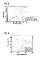
- Figures 7 and 8 depict the influence of the selection of a number of materials m1 for the spectral purity enhancement layer 104 (i.e. 110) on the reflectivity, and the influence of the thickness d (i.e. d1) of a spectral purity enhancement layer 110 of Si 3 N 4 on the reflectivity, respectively.
- These embodiments are all directed to a standard 50 layer Si/Mo multiplayer mirrors 100, with a top layer 103 of a certain material (e.g. Si).
- the percentages listed in the legend give the reflectivity for 13.5 nm EUV radiation; the values on the y-axis indicate the reflectivity (*100%).
- Figure 7 shows some theoretical examples of first spectral purity enhancement layers 110 on a multi-layer mirror 1 for the 100-200 nm range.
- Embodiments of good candidate materials m1 for first spectral purity enhancement layers 110 are amorphous carbon, diamond, SiC and Si 3 N 4 . Simulations indicate that a combination of high index of refraction in the target wavelength and a low absorption for EUV are desirable (see also above).
- the resulting reflectivity curves are a combination of the reflectivity curve for the multi-layer mirror 100 (i.e. the multi-layer stack 102) and the spectral purity enhancement layer 104 (i.e. in these embodiments first spectral purity enhancement layer 110).
- the reflectivity curve of the first spectral purity enhancement layer 110 also changes depending on the thickness (see also above; and Figure 6). Due to this, the wavelength with minimum reflectivity depends on the thickness of first spectral purity enhancement layer 110.
- Figure 8 shows another embodiment using Si 3 N 4 as first spectral purity enhancement layer 110 and a Si/Mo multi-layer stack 102 with varying thickness d1.
- a spectral purity enhancement layer 104 e.g. a spectral purity enhancement layer 1-4 only including a first spectral purity enhancement layer 110, LP-CVD, PE-CVD or other techniques may be used.
- LP-CVD a spectral purity enhancement layer 1-4 only including a first spectral purity enhancement layer 110
- PE-CVD PE-CVD or other techniques
- a model study was made by depositing a Si 3 N 4 layer on a silicon wafer in order to test the principle of SPE-layers in practice.
- a layer thickness d1 of 15 nm is chosen.
- the lowest theoretical reflectivity is about 10%, so the first spectral purity enhancement layer 110 does not work very well in this range, but the reflectivity loss is sufficient to be able to show proof-of-principle.
- the thickness d1 of the deposited Si 3 N 4 layer 110 was determined to be 13.5 nm (LP-CVD deposition time was 1 minute and 45 seconds), with an estimated RMS surface roughness of around 0.5 nm.
- Figure 9 shows the measured reflectivity curve for the Si 3 N 4 coated silicon-wafer, compared with the measured reflectivity curve for a bare silicon wafer. The theoretical curves from IMD are also shown. It is evident that the experimental first spectral purity enhancement layer 110 has a very good agreement with the calculated values, which demonstrates that the principle of the spectral purity enhancement layer 104 (in this embodiment only first spectral purity enhancement layer 110) works as expected.
- a cap layer 105 may be present on top of the spectral purity enhancement layer 104.
- the spectral filter top layer 104 further includes a cap layer 105 on top of the first spectral purity enhancement layer 110, including Ru and having a layer thickness d4 between 0.5 and 2.5 nm.
- a material m4 selected from BN, B 4 C, B, C (e.g. diamond-like carbon), TiN, Pd, Rh, Au, or C 2 F 4 .
- the first spectral purity enhancement layer 110 is further used as cap layer 105.
- Suitable materials m4 as for use as cap layer 105 may be selected from Si 3 N 4 , SiC, MgF 2 or LiF.
- the cap layer may provide a further protection against oxidation of chemical of physical attack by particles from the source or other particles or gasses present in, for example, a lithographic apparatus wherein the multi-layer mirror 100 according to the present invention is used.
- the spectral filter top layer 104 further includes a cap layer 105 on top of the first spectral purity enhancement layer 110, the cap layer 105 including a material m4 selected from Ru, BN, B 4 C, B, C (e.g. diamond-like carbon), TiN, Pd, Rh, Au, C 2 F 4 , Si 3 N 4 , SiC, MgF 2 or LiF, and having a layer thickness d4 between 0.5 and 11 nm.
- materials m1 of first spectral purity enhancement layer 110 includes a material different from material m4 of cap layer 105, for example m1 is Si 3 N 4 and m4 is Ru.
- FIG. 10 An example reflection (y-axis * 100%) of an embodiment with a cap layer 105 as a function of the wavelength of the radiation is shown in Figure 10, which depicts the influence of a cap layer 105 including Ru on a spectral purity enhancement layer 110 on the reflectivity.
- the normal suppression of light by a conventional multi-layer mirror 100 is not sufficient in the DUV range between 130 and 190 nm and that the current DUV intensity needs to be reduced to 10% of its current power. These are typical values that one might expect for an EUV lithography tool.
- the EUV lithography system contains typically 11 Si/Mo multi-layer mirrors.
- the first spectral purity enhancement layer 110 according to above described embodiments will be placed on some of these mirrors 100, e.g. on multi-layer stack top layer 103, in order to achieve enough suppression in the DUV range. Using a first spectral purity enhancement layer 110 provides flexibility in choosing the suppression and resulting losses for EUV light.
- a 5 nm Si 3 N 4 first spectral purity enhancement layer 110 is chosen.
- Figure 11 shows the suppression of DUV light for an increasing number (1-5) of first spectral purity enhancement layers 110, i.e. an increasing number of multi-layer mirrors 100 including such first spectral purity enhancement layer 110, and also shows the target of 10% reflectivity in the DUV range (horizontal dashed line). From Figure 11 it can be seen that two multi-layer mirrors with Ru-capped 5 nm Si 3 N 4 first spectral purity enhancement layer 110 are enough to reach the desired DUV suppression. In fact, with two first spectral purity enhancement layers 110 the DUV is reduced to below 15% for any wavelength in the range of 130-190 nm and the average reduction is down to 7%.
- the EUV losses caused by this can be calculated by comparing the reflectivity of two normal Ru-capped multi-layer mirrors 100 (R ⁇ 75% per mirror, total R tot ⁇ 56%) with two Ru-capped multi-layer mirrors 100 with 5 nm Si 3 N 4 first spectral purity enhancement layers 110 (R ⁇ 63 % per mirror, R tot ⁇ 40%), resulting in a loss of 16% for EUV light due to the first spectral purity enhancement layers 110.
- a normal spectral purity filter has 50% losses.
- the losses are 6% per multi-layer mirror 1, which means that the multi-layer mirror 1 reflectivity should be 69% instead of the calculated 63%.
- This extra EUV loss is due to interference effects occurring for the EUV wavelength.
- the Si 3 N 4 layer can be split into two parts, with a layer of for instance Mo in-between.
- the calculated EUV reflectivity for the mirror is 68%, completely in agreement with EUV absorption in the first spectral purity enhancement layer 110. This will be elucidated below in another aspect of the present invention.
- the multi-layer mirror 100 according to the present invention is a normal incidence mirror configured to reflect radiation having a wavelength selected from a first wavelength range of 5-20 nm.
- the multi-layer mirror 100 according to the present invention is a normal incidence Si/Mo multi-layer mirror configured to reflect radiation having a wavelength selected from the wavelength range of 12-15 nm, for example 13.5 nm EUV radiation.
- the present invention also provides a method for enlarging the ratio of radiation having a wavelength selected from a first wavelength range of 5-20 nm and radiation having a wavelength selected from a second wavelength range of 100-400 nm in a beam of radiation of a source emitting radiation in both wavelength ranges, by reflecting at least part of the beam of radiation of the source on a mirror.
- the lithographic apparatus includes two or more multi-layer mirrors 100 according to the present invention, which are placed as normal incidence mirrors in the beam of radiation produced by the source SO.
- a lithographic apparatus and/or a method are provided wherein a plurality of multi-layer mirrors 100 according to the present invention are used, e.g. in a further embodiment two or more, and wherein reflected radiation of a multi-layer mirror closest to a source in the beam of radiation generated by the source, is reflected on one or more next multi-layer mirrors 100, respectively.
- a lithographic apparatus and/or a method wherein the lithographic apparatus includes a plurality of multi-layer mirrors 100 as described above and wherein the materials m1 of the layers 104 (i.e. first spectral purity enhancement layer 110) and the layer thicknesses d (i.e. d1) of the layers 110 included in the spectral filter top layers 104 of the different multi-layer mirrors 100, respectively, are designed such as to: minimize absorption and/or destructive interference of radiation having a wavelength selected from a first wavelength range of 5-20 nm; and maximize absorption and/or destructive interference of radiation having a wavelength selected from a substantial part of the wavelength range of 100-400 nm.
- the filtering away of undesired wavelengths can be tuned such that desired wavelength, for example between 5 and 20 nm is not reduced substantially (e.g. less than about 50 % reduction with respect to the same multi-layer mirrors without such first spectral purity enhancement layers 110), whereas DUV radiation is reduced substantially (e.g. a reduction with 90 %, or about 95%, or even about 99% or more, with respect to the same multi-layer mirrors without such first spectral purity enhancement layers 110).
- Such a reduction may apply in an embodiment to a substantial part of the wavelength range of 100-400 nm, for example for 15% of the wavelength range between 100 and 400 nm, i.e. for at least about 15% of the wavelength range, the radiation reduction is at least about 90% of the total radiation at this about 15% part of the wavelength range. In an embodiment, at least the radiation at wavelengths between about 130 and 190 nm is reduced with about 90%, or more.
- one or more multi-layer mirrors 100 may be supplied with a spectral purity enhancement layer 104 designed for reduction of radiation having a wavelength in the range of 100-200 nm and one or more multi-layer mirrors 100 may be supplied with a spectral purity enhancement layer 104 designed for reduction of radiation having a wavelength in the range of 200-300 nm.
- a device manufacturing method including providing a beam of radiation; patterning the beam of radiation; projecting the patterned beam of radiation onto a target portion of a substrate; enlarging the ratio of radiation having a wavelength selected from a first wavelength range of 5-20 nm and radiation having a wavelength selected from a second wavelength range of 100-400 nm in a beam of radiation of a source emitting radiation in both wavelength ranges by reflecting at least part of the beam of radiation of the source on a mirror according to the embodiments as described above.
- a number of multi-layer mirrors 100 with first spectral purity enhancement layers 110 may be used.
- a multi-layer mirror 100 including a) a multi-layer stack 102, the multi-layer stack 102 including a plurality of alternating layers with a multi-layer stack top layer 103, and b) a spectral filter top layer 104 arranged on the multi-layer stack 103, the spectral filter top layer 104 including a first spectral purity enhancement layer 110 including a material m1 and having a layer thickness d1; an intermediate layer 111 including a material m2 and having a layer thickness d2; a second spectral purity enhancement layer 112 including a material m3 and having a layer thickness d3, the second spectral purity enhancement layer 112 being arranged on the multi-layer stack top layer 103.
- a thickness of the first spectral purity enhancement layer 110 may be determined for which the interference in the EUV does not give negative effects (see above embodiment with a spectral purity enhancement layer 104 including only a first spectral purity enhancement layer 110), for example a thickness for interference in the EUV regions does not occur (for example a 7 nm Si 3 N 4 layer may not have losses due to EUV interference), or one chooses the extra layer 111 in-between, which is described in the present embodiment (spectral filter top layer 104 including a first 110 and second 112 spectral purity enhancement layer 110 and an intermediate layer 111).
- first spectral purity enhancement layer 110 e.g. Si 3 N 4
- first spectral purity enhancement layer 110 is "split" into two parts, i.e. a first spectral purity enhancement layer 110 and a second spectral purity enhancement layer 112, with a intermediate layer 111, for example Mo, in-between.
- a first spectral purity enhancement layer 110 is "split" into two parts, i.e. a first spectral purity enhancement layer 110 and a second spectral purity enhancement layer 112, with a intermediate layer 111, for example Mo, in-between.
- the calculated EUV reflectivity for the mirror 100 can be 68%, assuming Si 3 N 4 , completely in agreement with EUV absorption in the first spectral purity enhancement layer 110.
- split spectral purity enhancement layer refers to the embodiment as depicted in Figure 4a: one first spectral purity enhancement layer 110, and intermediate layer 111 and a second spectral purity enhancement layer 112.
- Figure 11 shows the same calculation as shown with the solid curves (i.e.
- one or more multi-layer mirrors 100 each having a spectral purity enhancement layer 104 including only a first spectral purity enhancement layer 110), but in this case with a first spectral purity enhancement layer 110 of 2.5 nm Si 3 N 4 , followed by an intermediate layer 111 of 2 nm Mo, followed by a second spectral purity enhancement layer 112 of 2.5 nm Si 3 N 4 , followed by a 2.5 nm Ru cap layer 105.
- the curves look very similar, but the dotted curve have slightly less DUV suppression and is slightly shifted to shorter wavelengths.
- three multi-layer mirrors 100 with the spectral purity enhancement layer of this embodiment may be needed in order to reach suppression below 10%, but the total losses are much lower, namely 11% EUV loss with an average DUV suppression down to 3.4% (three Ru-capped mirrors R tot ⁇ 42%; 3 Mo-split spectral purity enhancement layers 110 and 112 Ru-capped mirrors R tot ⁇ 31%).
- the total losses for EUV are 50%, with an average DUV reduction down to 0.7% (roughly two orders of magnitude).
- a maximum of seven spectral purity enhancement layers 110+112 i.e. seven spectral purity enhancement layers 104, each including layers 110, 111 and 112, and each being arranged on different multi-layer mirrors 100, respectively
- the thickness of d1+d2 is approximately the same as the thickness of d1 as given in the above described embodiment and as indicated in the embodiments of Table 1.
- the present embodiment may use a Ru cap layer 105.
- a multi-layer mirror 100 including a) a multi-layer stack 102, the multi-layer stack 102 including a plurality of alternating layers with a multi-layer stack top layer 103, and b) a spectral filter top layer 104 arranged on the multi-layer stack 102, the spectral filter top layer 104 including a first spectral purity enhancement layer 110 including a material m1 and having a layer thickness d1; an intermediate layer 111 including a material m2 and having a layer thickness d2; a second spectral purity enhancement layer 112 including a material m3 and having a layer thickness d3, the second spectral purity enhancement layer 112 being arranged on the multi-layer stack top layer 103, wherein the first 110 and second 112 spectral purity enhancement layers include independently a material (m1 and m3, respectively) selected from Si 3 N4, SiO 2 , ZnS, Te, diamond, CsI, Se, SiC,
- the multi-layer mirror 100 further optionally includes a cap layer 105 on top of the first spectral purity enhancement layer 104, including Ru and having a layer thickness d4 between 0.5 and 2.5 nm.
- the present invention provides a multi-layer mirror 100, wherein the intermediate layer includes a metal.
- the intermediate layer includes a material m2 selected from Be, B, C, Si, P, S, K, Ca, Sc, Br, Rb, Sr, Y, Zr, Nb, Mo, Ba, La, Ce, Pr, Pa or U.
- a multi-layer mirror 100 wherein the first spectral purity enhancement layer 110 and the second spectral purity enhancement layer 112 have an imaginary part of the complex index of refraction k ⁇ 0.25*n + 1.07, wherein n is the real part of the complex index of refraction.
- real part of the complex index of refraction is equal or larger than 1.5 and the imaginary part of the complex index of refraction is equal or smaller than 2.
- the first spectral purity enhancement layer 110 and the second spectral purity enhancement layer 112 have a real part of the complex index of refraction equal or larger than 2 and a imaginary part of the complex index of refraction is equal or smaller than 1.6.
- the indices of refraction here refer to indices of refraction at a radiation wavelength or within a radiation wavelength range selected from the range of 100-400 nm, and in a embodiment between 100 and 200 nm.
- materials and layer thicknesses of the respective layers are selected fulfilling the criteria as described herein.
- a multi-layer mirror 100 including a) a multi-layer stack 102, the multi-layer stack 102 including a plurality of alternating layers with a multi-layer stack top layer 103, and b) a spectral filter top layer 104 arranged on the multi-layer stack 102, the spectral filter top layer 104 including a first spectral purity enhancement layer 110 including a material m1 and having a layer thickness d1; an intermediate layer 111 including a material m2 and having a layer thickness d2; a second spectral purity enhancement layer 112 including a material m3 and having a layer thickness d3, the second spectral purity enhancement layer 112 being arranged on the multi-layer stack top layer 103, wherein the first 110 and second 112 spectral purity enhancement layers include independently a material (m1 and m3, respectively) having an imaginary part of the complex index of refraction k ⁇ 0.25*n + 1.07, wherein
- a multi-layer mirror 100 including a) a multi-layer stack 102, the multi-layer stack 102 including a plurality of alternating layers with a multi-layer stack top layer 103, and b) a spectral filter top layer 104 arranged on the multi-layer stack 102, the spectral filter top layer 104 including a first spectral purity enhancement layer 110 including a material m1 and having a layer thickness d1; an intermediate layer 111 including a material m2 and having a layer thickness d2; a second spectral purity enhancement layer 112 including a material m3 and having a layer thickness d3, the second spectral purity enhancement layer 112 being arranged on the multi-layer stack top layer 103, wherein the first 110 and second 112 spectral purity enhancement layers include independently a material (m1 and m3, respectively) having a real part of the complex index of refraction equal or larger than 2 and a imaginary part of the complex
- a multi-layer mirror 100 wherein the materials (ml, m2 and m3, respectively) of the layers and the layer thicknesses (d1, d2 and d3, respectively) of the layers included in the spectral filter top layer are designed such as to minimize absorption and/or destructive interference of radiation having a wavelength selected from a first wavelength range of 5-20 nm, and maximize absorption and/or destructive interference of radiation having a wavelength selected from a second wavelength range of 100-400 nm.
- a multi-layer mirror 100 wherein the first 110 and second 112 spectral purity enhancement layers include Si 3 N 4 , each layer independently having a layer thickness d1 and d3, respectively, between 1.5 and 3.5 nm, and wherein the intermediate layer 111 includes Mo, having a layer thickness d2 between 1 and 3 nm.
- Alternative embodiments may have the same dimensions but with m1 and m2 each independently selected from Si 3 N 4 , SiO 2 , ZnS, Te, diamond, CsI, Se, SiC, amorphous carbon, MgF 2 , CaF 2 , TiO 2 Ge, PbF 2 , ZrO 2 BaTiO 3 , LiF or NaF.
- the multi-layer mirror 100 according to the present invention is a normal incidence mirror configured to reflect radiation having a wavelength selected from a first wavelength range of 5-20 nm.
- the multi-layer mirror 100 according to the present invention is a normal incidence Si/Mo multi-layer mirror configured to reflect radiation having a wavelength selected from the wavelength range of 12-15 nm, for example 13.5 nm EUV radiation.
- the present invention also provides a method for enlarging the ratio of radiation having a wavelength selected from a first wavelength range of 5-20 nm and radiation having a wavelength selected from a second wavelength range of 100-400 nm in a beam of radiation of a source emitting radiation in both wavelength ranges, by reflecting at least part of the beam of radiation of the source on a mirror according to this embodiment.
- the lithographic apparatus includes two or more multi-layer mirrors 100 according to the present invention, which are placed as normal incidence mirrors in the radiation produced by the source SO.
- a lithographic apparatus and/or a method are provided wherein a plurality of multi-layer mirrors 100 according to the present invention are used, for example in a further embodiment two or more, and wherein reflected radiation of a multi-layer mirror closest to a source in the radiation generated by the source, is reflected on one or more next multi-layer mirrors 100, respectively.
- a lithographic apparatus an/or a method, wherein the lithographic apparatus includes a plurality of multi-layer mirrors 100 as described above and wherein the materials m1, m2 and m3, respectively of the first spectral purity enhancement layer 110, intermediate layer 111 and second spectral purity enhancement layer 112, respectively, included in spectral purity enhancement layer 104 and the layer thicknesses d1, d2 and d3 of the layers 110, 111 and 112, respectively, included in the spectral filter top layers 104 of the different multi-layer mirrors 100, respectively, are designed to minimize absorption and/or destructive interference of radiation having a wavelength selected from a first wavelength range of 5-20 nm, and maximize absorption and/or destructive interference of radiation having a wavelength selected from a substantial part of the wavelength range of 100-400 nm.
- the filtering away of undesired wavelengths can be tuned such that desired radiation, for example with a wavelength between 5 and 20 nm, is not reduced substantially (e.g.
- a reduction preferably applies in an embodiment to a substantial part of the wavelength range of 100-400 nm, e.g. for 15% of the wavelength range between 100 and 400 nm.
- at least the radiation at wavelengths between about 130 and 190 nm is reduced with about 90%, or more.
- one or more multi-layer mirrors 100 may be supplied with a spectral purity enhancement layer 104 designed for reduction of radiation having a wavelength in the range of 100-200 nm and one or more multi-layer mirrors 100 may be supplied with a spectral purity enhancement layer 104 designed for reduction of radiation having a wavelength in the range of 200-300 nm.
- a device manufacturing method including providing a beam of radiation; patterning the beam of radiation; projecting the patterned beam of radiation onto a target portion of a substrate; enlarging the ratio of radiation having a wavelength selected from a first wavelength range of 5-20 nm and radiation having a wavelength selected from a second wavelength range of 100-400 nm in a beam of radiation of a source emitting radiation in both wavelength ranges by reflecting at least part of the beam of radiation of the source on a mirror according to the embodiments as described above.
- the spectral purity enhancement layer 104 includes only a first spectral purity enhancement layer 110 and an intermediate layer 111, wherein the latter is positioned on the multi-layer stack top layer 103.
- a multi-layer mirror 100 including a) a multi-layer stack 102, the multi-layer stack 102 including a plurality of alternating layers with a multi-layer stack top layer 103, and b) a spectral filter top layer 104 arranged on the multi-layer stack 103, the spectral filter top layer 104 including a first spectral purity enhancement layer 110 including a material m1 and having a layer thickness d1; an intermediate layer 111 including a material m2 and having a layer thickness d2, the intermediate layer 111 being arranged on the multi-layer stack top layer 103.
- the present embodiment may be combined with the optional cap layer 105, for example Ru having a layer thickness d4 between 0.5 and 2.5 nm.
- the multi-layer mirror 100 further optionally includes a cap layer 105 on top of the first spectral purity enhancement layer 104, including Ru and having a layer thickness d4 between 0.5 and 2.5 nm.
- a multi-layer mirror 100 including a) a multi-layer stack 102, the multi-layer stack 102 including a plurality of alternating layers with a multi-layer stack top layer 103, and b) a spectral filter top layer 104 arranged on the multi-layer stack 102, the spectral filter top layer 104 including a first spectral purity enhancement layer 110 including a material m1 and having a layer thickness d1; an intermediate layer 111 including a material m2 and having a layer thickness d2, the intermediate layer 111 being arranged on the multi-layer stack top layer 103, wherein the first spectral purity enhancement layer 110 includes a material m1 selected from Si 3 N 4 , SiO 2 , ZnS, Te, diamond, CsI, Se, SiC, amorphous carbon, MgF 2 , CaF 2 , TiO2, Ge, PbF 2 , ZrO 2 , BaTiO 3 , Li
- the present invention provides a multi-layer mirror 100, wherein the intermediate layer 111 includes a metal.
- the intermediate layer 111 includes a material m2 selected from Be, B, C, Si, P, S, K, Ca, Sc, Br, Rb, Sr, Y, Zr, Nb, Mo, Ba, La, Ce, Pr, Pa or U.
- a multi-layer mirror 100 wherein the first spectral purity enhancement layer 110 has an imaginary part of the complex index of refraction k ⁇ 0.25*n + 1.07, wherein n is the real part of the complex index of refraction.
- real part of the complex index of refraction is equal or larger than 1.5 and the imaginary part of the complex index of refraction is equal or smaller than 2.
- the first spectral purity enhancement layer 110 has a real part of the complex index of refraction equal or larger than 2 and a imaginary part of the complex index of refraction is equal or smaller than 1.6.
- the indices of refraction here refer to indices of refraction at a radiation wavelength or within a radiation wavelength range selected from the range of 100-400 nm, and in a embodiment between 100 and 200 nm.
- materials and layer thicknesses of the respective layers are selected fulfilling the criteria as described herein.
- a multi-layer mirror 100 including a) a multi-layer stack 102, the multi-layer stack 102 including a plurality of alternating layers with a multi-layer stack top layer 103, and b) a spectral filter top layer 104 arranged on the multi-layer stack 102, the spectral filter top layer 104 including a first spectral purity enhancement layer 110 including a material m1 and having a layer thickness d1; an intermediate layer 111 including a material m2 and having a layer thickness d2, the intermediate layer 111 being arranged on the multi-layer stack top layer 103, wherein the first spectral purity enhancement layer 110 includes a material m1 having a complex index of refraction k ⁇ 0.25*n + 1.07, n is the real part of the complex index of refraction, the intermediate layer 111 includes a material m2 different from material m1 of the first spectral purity enhancement layer 110, and the spectral
- a multi-layer mirror 100 including a) a multi-layer stack 102, the multi-layer stack 102 including a plurality of alternating layers with a multi-layer stack top layer 103, and b) a spectral filter top layer 104 arranged on the multi-layer stack 102, the spectral filter top layer 104 including a first spectral purity enhancement layer 110 including a material m1 and having a layer thickness d1; an intermediate layer 111 including a material m2 and having a layer thickness d2, the intermediate layer 111 being arranged on the multi-layer stack top layer 103, wherein the first spectral purity enhancement layer 110 includes a material m1 having a real part of the complex index of refraction equal or larger than 2 and a imaginary part of the complex index of refraction is equal or smaller than 1.6, wherein the intermediate layer 111 includes a material m2 different from material m1 of the first spectral purity enhancement layer 110 and
- a multi-layer mirror 100 wherein the materials (m1 and m2, respectively) of the layers and the layer thicknesses (d1 and d2, respectively) of the layers included in the spectral filter top layer are designed to minimize absorption and/or destructive interference of radiation having a wavelength selected from a first wavelength range of 5-20 nm, and maximize absorption and/or destructive interference of radiation having a wavelength selected from a second wavelength range of 100-400 nm.
- a multi-layer mirror 100 wherein the first 110 spectral purity enhancement layer includes Si 3 N 4 , having a layer thickness d1 between 4 and 1 nm, and wherein the intermediate layer 111 includes Mo, having a layer thickness d2 between 1 and 3 nm.
- the multi-layer mirror 100 according to the present invention is a normal incidence mirror configured to reflect radiation having a wavelength selected from a first wavelength range of 5-20 nm.
- the multi-layer mirror 100 according to the present invention is a normal incidence Si/Mo multi-layer mirror configured to reflect radiation having a wavelength selected from the wavelength range of 12-15 nm, e.g. 13.5 nm EUV radiation.
- the present invention also provides a method for enlarging the ratio of radiation having a wavelength selected from a first wavelength range of 5-20 nm and radiation having a wavelength selected from a second wavelength range of 100-400 nm in a beam of radiation of a source emitting radiation in both wavelength ranges, by reflecting at least part of the beam of radiation of the source on a mirror.
- the lithographic apparatus includes two or more multi-layer mirrors 100 according to the present invention, which are placed as normal incidence mirrors in the radiation produced by the source SO.
- a lithographic apparatus and/or a method are provided wherein a plurality of multi-layer mirrors 100 according to the present invention are used, for example in a further embodiment two or more, and wherein reflected radiation of a multi-layer mirror closest to a source in the radiation generated by the source is reflected on one or more next multi-layer mirrors 100, respectively.
- a lithographic apparatus and/or a method wherein the lithographic apparatus includes a plurality of multi-layer mirrors 100 as described above and wherein the materials m1 and m2, of the layers first spectral purity enhancement layer 110 and intermediate layer 111, respectively, included in spectral purity enhancement layer 104 and the layer thicknesses d1 and d2, of the layers 110 and 111, respectively, included in the spectral filter top layers 104 of the different multi-layer mirrors 100, respectively, are designed to minimize absorption and/or destructive interference of radiation having a wavelength selected from a first wavelength range of 5-20 nm, and maximize absorption and/or destructive interference of radiation having a wavelength selected from a substantial part of the wavelength range of 100-400 nm.
- the filtering away of undesired wavelengths can be tuned such that desired wavelength, for example between 5 and 20 nm is not reduced substantially (e.g. less than about 50 % reduction with respect to the same multi-layer mirrors without such first spectral purity enhancement layers 110), whereas DUV radiation is reduced substantially (e.g.
- Such a reduction may apply in an embodiment to a substantial part of the wavelength range of 100-400 nm, e.g. for about 15% of the wavelength range between 100 and 400 nm.
- at least the radiation at wavelengths between about 130 and 190 nm is reduced with about 90%, or more.
- one or more multi-layer mirrors 100 may be supplied with a spectral purity enhancement layer 104 designed for reduction of radiation having a wavelength in the range of 100-200 nm and one or more multi-layer mirrors 100 may be supplied with a spectral purity enhancement layer 104 designed for reduction of radiation having a wavelength in the range of 200-300 nm.
- a device manufacturing method including providing a beam of radiation using the illumination system; patterning the beam of radiation; projecting the patterned beam of radiation onto a target portion of the substrate; enlarging the ratio of radiation having a wavelength selected from a first wavelength range of 5-20 nm and radiation having a wavelength selected from a second wavelength range of 100-400 nm in radiation of a source emitting radiation in both wavelength ranges by reflecting at least part of the radiation of the source on a mirror according to the embodiments as described above.
- a lithographic apparatus a method for enlarging the ratio of desired (EUV) to undesired (DUV) radiation and/or a device manufacturing method, wherein two or more multi-layer mirrors 100 selected from the three embodiments as described above are used.
- one or more multi-layer mirrors 100 may be supplied with a spectral purity enhancement layer 104 designed for reduction of radiation having a wavelength in the range of 100-200 nm and one or more multi-layer mirrors 100 may be supplied with a spectral purity enhancement layer 104 designed for reduction of radiation having a wavelength in the range of 200-300 nm.
- first spectral purity enhancement layer 110 may also be applied.
- this may be a multi-layer mirror 100 including a multi-layer stack 102 with on top of the multi-layer stack top layer 103 one or more selected of the following layer stacks (wherein the first (most left) number represents the layer arranged on the multi-layer stack top layer 103, and wherein n symbolizes the number of repeating the layer combinations): (110/111) n , (111/110) n , (110/111) n /110, and (111/110) n /110.
- a cap layer 105 may be provided on the final layer (the last (most right) number), e.g. schematically: 102/(110/111) n /110/105.
- multi-layer mirror 100 may include a multi-layer (mirror) stack 102, e.g. including a number of alternating Mo/Si, or W/Si or WRe/Si, or other type of multi-layer stack, wherein multi-layer stack top layer 103 may include, for example Mo, Si, W, or WRe, etc.
- the spectral filter top layer 104 is arranged, which may further optionally be capped with a cap layer 105 including a material m4 selected from Ru, BN, B 4 C, B, C (e.g.
- cap layer 105 includes Ru, having a layer thickness d4 between 0.5 and 2.5 nm.
- this multi-layer stack top layer 103 does not represent one of the layers of the multi-layer stack 102, but represents a cap layer, including a material m5 selected from Ru, BN, B 4 C, B, C (e.g. diamond-like carbon), TiN, Pd, Rh, Au, C 2 F 4 , Si 3 N 4 , SiC, MgF 2 or LiF, having a layer thickness d5 between 0.5 and 11 nm.
- a material m5 selected from Ru, BN, B 4 C, B, C (e.g. diamond-like carbon), TiN, Pd, Rh, Au, C 2 F 4 , Si 3 N 4 , SiC, MgF 2 or LiF, having a layer thickness d5 between 0.5 and 11 nm.
- multi-layer mirror 100 includes a) a multi-layer mirror stack 102, the multi-layer stack 102 including a plurality of alternating layers with a multi-layer stack top layer 103, wherein multi-layer stack top layer 103 represents a cap layer (with layer thickness d5) and b) a spectral filter top layer 104 arranged on the multi-layer stack 102, wherein this spectral filter top layer 104 is a spectral filter top layer 104 according to one of the above described embodiments.
- material m5 of cap layer/multi-layer stack top layer 103 is not the same material as material m1 of first spectral purity enhancement layer 110.
- a multi-layer mirror 100 including a) a multi-layer stack 102, the multi-layer stack 102 including a plurality of alternating layers with a multi-layer stack top layer 103, wherein multi-layer stack top layer 103 represents a cap layer, and b) a spectral filter top layer 104 arranged on the multi-layer stack 102, the spectral filter top layer 104 including a first spectral purity enhancement layer 110 including a material m1 and having a layer thickness d1, being arranged on the multi-layer stack top layer 103, wherein the first spectral purity enhancement layer 110 includes a material m1 selected from Si 3 N 4 , SiO 2 , ZnS, Te, diamond, CsI, Se, SiC, amorphous carbon, MgF 2 , CaF 2 , TiO 2 , Ge, PbF 2 , ZrO 2 , BaTiO 3 , LiF or NaF, the spectral filter top layer 110 has
- the multi-layer stack top layer 103 includes Ru and has a layer thickness d5 between 0.5 and 2.5 nm.
- Spectral filter top layer 110 includes in an embodiment a layer thickness d1 of 4-11 nm Si 3 N 4 (m5), and in a variation 5-7 nm Si 3 N 4 (m5).
- a second cap layer 105 may be present, arranged on spectral filter top layer 104 (as shown in Figures 3 and 4a).
- a spectral purity enhancement layer 104 is suited to suppress light in a certain target wavelength range, such as the DUV range between 130 and 190 nm.
- a typical suppression of more than 1 order of magnitude can be achieved in the DUV region from 130-190 nm, using two mirrors with spectral purity enhancement layers 104, including a cap layer 105 of e.g. Ru. Without the Ru cap layer 105, even better suppression can be achieved with lower losses.
- a cap layer 105 of e.g. Ru e.g. Ru
- EUV loss can be reduced by splitting the spectral purity enhancement layer 104 in two parts, as described above and schematically depicted in Figure 4a.
- the spectral purity enhancement layer 104 can also act as a cap-layer to protect the multi-layer mirror 100 against oxidation.
- Different materials can be used for different wavelengths.
- Different spectral purity enhancement layers 104 can be used on different mirrors in order to achieve a broader absorption range (with different materials), or a stronger suppression (with the same material as spectral purity enhancement layer).
- the spectral purity enhancement layer 104 normally does not lead to extra reflectivity for wavelengths other than the target wavelength range.
- spectral purity enhancement layer 104 has the advantage of high flexibility, because one can choose the number of spectral purity enhancement layers 104 (and therefore the losses) depending on the suppression that is required.
- the spectral purity enhancement layers 104 can be added at any time.
- lithographic apparatus in the manufacture of ICs
- the lithographic apparatus described herein may have other applications, such as the manufacture of integrated optical systems, guidance and detection patterns for magnetic domain memories, flat-panel displays, liquid-crystal displays (LCDs), thin-film magnetic heads, etc.
- any use of the terms “wafer” or “die” herein may be considered as synonymous with the more general terms “substrate” or “target portion”, respectively.
- the substrate referred to herein may be processed, before or after exposure, in for example a track (a tool that typically applies a layer of resist to a substrate and develops the exposed resist), a metrology tool and/or an inspection tool. Where applicable, the disclosure herein may be applied to such and other substrate processing tools. Further, the substrate may be processed more than once, for example in order to create a multi-layer IC, so that the term substrate used herein may also refer to a substrate that already contains multiple processed layers.
- imprint lithography a topography in a patterning device defines the pattern created on a substrate.
- the topography of the patterning device may be pressed into a layer of resist supplied to the substrate whereupon the resist is cured by applying electromagnetic radiation, heat, pressure or a combination thereof.
- the patterning device is moved out of the resist leaving a pattern in it after the resist is cured.
- the present invention may take the form of a computer program containing one or more sequences of machine-readable instructions describing a method as disclosed above, or a data storage medium (e.g. semiconductor memory, magnetic or optical disk) having such a computer program stored therein.
- a data storage medium e.g. semiconductor memory, magnetic or optical disk
- a material m1 (and where applicable m3) is selected that fulfills both these criteria.
- material m1 of first spectral purity enhancement layer 110 (and where applicable material m3 of second spectral purity enhancement layer 112) has a real part of the complex index of refraction equal or larger than 2 and a imaginary part of the complex index of refraction is equal or smaller than 1.6.
- silicon nitride is referred to as Si 3 N 4 . However, this should be interpreted as including all Si-N compounds, such as SiN.
- the present invention is not limited to application of the lithographic apparatus or use in the lithographic apparatus as described in the embodiments. Further, the drawings usually only include the elements and features that are necessary to understand the present invention. Beyond that, the drawings of the lithographic apparatus are schematic and not to scale. The present invention is not limited to those elements, shown in the schematic drawings (e.g. the number of mirrors drawn in the schematic drawings). Further, the present invention is not confined to the lithographic apparatus described in Figures 1 and 2.
Landscapes
- Physics & Mathematics (AREA)
- General Physics & Mathematics (AREA)
- Engineering & Computer Science (AREA)
- Optics & Photonics (AREA)
- Chemical & Material Sciences (AREA)
- Nanotechnology (AREA)
- Crystallography & Structural Chemistry (AREA)
- High Energy & Nuclear Physics (AREA)
- Public Health (AREA)
- General Engineering & Computer Science (AREA)
- Spectroscopy & Molecular Physics (AREA)
- Health & Medical Sciences (AREA)
- Environmental & Geological Engineering (AREA)
- Epidemiology (AREA)
- Theoretical Computer Science (AREA)
- Manufacturing & Machinery (AREA)
- Condensed Matter Physics & Semiconductors (AREA)
- Mathematical Physics (AREA)
- Plasma & Fusion (AREA)
- Exposure And Positioning Against Photoresist Photosensitive Materials (AREA)
- Exposure Of Semiconductors, Excluding Electron Or Ion Beam Exposure (AREA)
- Optical Elements Other Than Lenses (AREA)
- Optical Filters (AREA)
Priority Applications (2)
| Application Number | Priority Date | Filing Date | Title |
|---|---|---|---|
| EP10181596A EP2261698B1 (de) | 2005-04-27 | 2006-04-26 | Spektraler Reinigungsfilter für einen mehrschichtigen Spiegel, lithografische Vorrichtung mit einem derartigen mehrschichtigen Spiegel, Verfahren zur Vergrößerung des Verhältnisses von erwünschter und unerwünschter Strahlung sowie Geräteherstellungsverfahren |
| EP10181598A EP2261699B1 (de) | 2005-04-27 | 2006-04-26 | Spektraler Reinigungsfilter für einen mehrschichtigen Spiegel, lithografische Vorrichtung mit einem derartigen mehrschichtigen Spiegel, Verfahren zur Vergrößerung des Verhältnisses von erwünschter und unerwünschter Strahlung sowie Geräteherstellungsverfahren |
Applications Claiming Priority (1)
| Application Number | Priority Date | Filing Date | Title |
|---|---|---|---|
| US11/115,406 US7336416B2 (en) | 2005-04-27 | 2005-04-27 | Spectral purity filter for multi-layer mirror, lithographic apparatus including such multi-layer mirror, method for enlarging the ratio of desired radiation and undesired radiation, and device manufacturing method |
Related Child Applications (2)
| Application Number | Title | Priority Date | Filing Date |
|---|---|---|---|
| EP10181596.7 Division-Into | 2010-09-29 | ||
| EP10181598.3 Division-Into | 2010-09-29 |
Publications (2)
| Publication Number | Publication Date |
|---|---|
| EP1717609A1 true EP1717609A1 (de) | 2006-11-02 |
| EP1717609B1 EP1717609B1 (de) | 2012-04-11 |
Family
ID=36764463
Family Applications (3)
| Application Number | Title | Priority Date | Filing Date |
|---|---|---|---|
| EP10181598A Expired - Lifetime EP2261699B1 (de) | 2005-04-27 | 2006-04-26 | Spektraler Reinigungsfilter für einen mehrschichtigen Spiegel, lithografische Vorrichtung mit einem derartigen mehrschichtigen Spiegel, Verfahren zur Vergrößerung des Verhältnisses von erwünschter und unerwünschter Strahlung sowie Geräteherstellungsverfahren |
| EP10181596A Expired - Lifetime EP2261698B1 (de) | 2005-04-27 | 2006-04-26 | Spektraler Reinigungsfilter für einen mehrschichtigen Spiegel, lithografische Vorrichtung mit einem derartigen mehrschichtigen Spiegel, Verfahren zur Vergrößerung des Verhältnisses von erwünschter und unerwünschter Strahlung sowie Geräteherstellungsverfahren |
| EP06113136A Expired - Lifetime EP1717609B1 (de) | 2005-04-27 | 2006-04-26 | Spektraler Reinigungsfilter für einen mehrschichtigen Spiegel, lithografische Vorrichtung mit einem derartigen mehrschichtigen Spiegel, Verfahren zur Vergrößerung des Verhältnisses von erwünschter und unerwünschter Strahlung sowie Geräteherstellungsverfahren |
Family Applications Before (2)
| Application Number | Title | Priority Date | Filing Date |
|---|---|---|---|
| EP10181598A Expired - Lifetime EP2261699B1 (de) | 2005-04-27 | 2006-04-26 | Spektraler Reinigungsfilter für einen mehrschichtigen Spiegel, lithografische Vorrichtung mit einem derartigen mehrschichtigen Spiegel, Verfahren zur Vergrößerung des Verhältnisses von erwünschter und unerwünschter Strahlung sowie Geräteherstellungsverfahren |
| EP10181596A Expired - Lifetime EP2261698B1 (de) | 2005-04-27 | 2006-04-26 | Spektraler Reinigungsfilter für einen mehrschichtigen Spiegel, lithografische Vorrichtung mit einem derartigen mehrschichtigen Spiegel, Verfahren zur Vergrößerung des Verhältnisses von erwünschter und unerwünschter Strahlung sowie Geräteherstellungsverfahren |
Country Status (8)
| Country | Link |
|---|---|
| US (5) | US7336416B2 (de) |
| EP (3) | EP2261699B1 (de) |
| JP (2) | JP2006310793A (de) |
| KR (1) | KR100779699B1 (de) |
| CN (1) | CN100559217C (de) |
| AT (1) | ATE553403T1 (de) |
| SG (1) | SG126906A1 (de) |
| TW (1) | TWI302992B (de) |
Cited By (9)
| Publication number | Priority date | Publication date | Assignee | Title |
|---|---|---|---|---|
| WO2010022839A3 (en) * | 2008-08-28 | 2010-06-03 | Asml Netherlands B.V. | Spectral purity filter and lithographic apparatus |
| WO2011117009A1 (en) * | 2010-03-24 | 2011-09-29 | Asml Netherlands B.V. | Lithographic apparatus and spectral purity filter |
| US8121254B2 (en) | 2007-01-25 | 2012-02-21 | Nikon Corporation | Optical element, exposure apparatus using this, and device manufacturing method |
| WO2012119672A1 (en) | 2011-03-04 | 2012-09-13 | Asml Netherlands B.V. | Lithograpic apparatus, spectral purity filter and device manufacturing method |
| EP2511944A4 (de) * | 2009-12-09 | 2014-09-03 | Asahi Glass Co Ltd | Mit einer reflektierenden schicht ausgestattetes substrat für die euv-lithographie, reflektierender maskenrohling für die euv-lithographie, reflektierende maske für die euv-lithographie und verfahren zur herstellung des mit einer reflektierenden schicht ausgestatteten substrats |
| WO2015058931A1 (de) * | 2013-10-23 | 2015-04-30 | Carl Zeiss Smt Gmbh | Vielschichtstruktur für euv-spiegel |
| WO2015062919A1 (de) * | 2013-11-04 | 2015-05-07 | Carl Zeiss Smt Gmbh | Spiegel, insbesondere für eine mikrolithographische projektionsbelichtungsanlage |
| WO2015086419A1 (en) * | 2013-12-09 | 2015-06-18 | Element Six Technologies Limited | Synthetic diamond optical mirrors |
| US11112672B2 (en) | 2015-10-16 | 2021-09-07 | Oxford University Innovation Limited | Optical device |
Families Citing this family (76)
| Publication number | Priority date | Publication date | Assignee | Title |
|---|---|---|---|---|
| US7843632B2 (en) * | 2006-08-16 | 2010-11-30 | Cymer, Inc. | EUV optics |
| DE10309084A1 (de) | 2003-03-03 | 2004-09-16 | Carl Zeiss Smt Ag | Reflektives optisches Element und EUV-Lithographiegerät |
| JP4532991B2 (ja) * | 2004-05-26 | 2010-08-25 | キヤノン株式会社 | 投影光学系、露光装置及びデバイス製造方法 |
| US7336416B2 (en) * | 2005-04-27 | 2008-02-26 | Asml Netherlands B.V. | Spectral purity filter for multi-layer mirror, lithographic apparatus including such multi-layer mirror, method for enlarging the ratio of desired radiation and undesired radiation, and device manufacturing method |
| US7518797B2 (en) * | 2005-12-02 | 2009-04-14 | Carl Zeiss Smt Ag | Microlithographic exposure apparatus |
| US7329876B2 (en) * | 2006-01-26 | 2008-02-12 | Xtreme Technologies Gmbh | Narrow-band transmission filter for EUV radiation |
| US7736820B2 (en) * | 2006-05-05 | 2010-06-15 | Asml Netherlands B.V. | Anti-reflection coating for an EUV mask |
| US7666555B2 (en) * | 2006-12-29 | 2010-02-23 | Intel Corporation | Pellicle, methods of fabrication and methods of use for extreme ultraviolet lithography |
| US7965378B2 (en) * | 2007-02-20 | 2011-06-21 | Asml Holding N.V | Optical system and method for illumination of reflective spatial light modulators in maskless lithography |
| US20080266651A1 (en) * | 2007-04-24 | 2008-10-30 | Katsuhiko Murakami | Optical apparatus, multilayer-film reflective mirror, exposure apparatus, and device |
| DE102007051671A1 (de) | 2007-10-26 | 2009-05-07 | Carl Zeiss Smt Ag | Abbildende Optik sowie Projektionsbelichtungsanlage für die Mikrolithographie mit einer derartigen abbildenden Optik |
| US20090250637A1 (en) * | 2008-04-02 | 2009-10-08 | Cymer, Inc. | System and methods for filtering out-of-band radiation in EUV exposure tools |
| TWI420134B (zh) * | 2008-05-09 | 2013-12-21 | Hon Hai Prec Ind Co Ltd | 光學鏡片及其鍍膜方法 |
| WO2009147014A1 (en) * | 2008-06-04 | 2009-12-10 | Asml Netherlands B.V. | Multilayer mirror and lithographic apparatus |
| JP5067483B2 (ja) * | 2008-06-19 | 2012-11-07 | 旭硝子株式会社 | Euvリソグラフィ用反射型マスクブランク |
| NL2002968A1 (nl) * | 2008-06-30 | 2009-12-31 | Asml Netherlands Bv | Optical element, lithographic apparatus including such an optical element, device manufacturing method, and device manufactured thereby. |
| EP2326990B1 (de) | 2008-07-11 | 2013-03-13 | ASML Netherlands BV | Spektraler reinheitsfilter, strahlungsquelle, lithografischer apparat und verfahren zur herstellung einer vorrichtung |
| KR101607228B1 (ko) * | 2008-08-14 | 2016-03-29 | 에이에스엠엘 네델란즈 비.브이. | 방사선 소스, 리소그래피 장치 및 디바이스 제조 방법 |
| NL2003303A (en) * | 2008-08-29 | 2010-03-11 | Asml Netherlands Bv | Spectral purity filter, lithographic apparatus including such a spectral purity filter, device manufacturing method, and device manufactured thereby. |
| WO2010032753A1 (ja) * | 2008-09-18 | 2010-03-25 | 株式会社ニコン | 開口絞り、光学系、露光装置及び電子デバイスの製造方法 |
| IT1395244B1 (it) * | 2008-12-17 | 2012-09-05 | St Microelectronics Srl | Procedimento di fabbricazione di un dispositivo emettitore di radiazione ottica a cavita' risonante |
| KR101694283B1 (ko) | 2009-02-13 | 2017-01-09 | 에이에스엠엘 네델란즈 비.브이. | 다층 거울 및 리소그래피 장치 |
| DE102009032779A1 (de) * | 2009-07-10 | 2011-01-13 | Carl Zeiss Smt Ag | Spiegel für den EUV-Wellenlängenbereich, Projektionsobjektiv für die Mikrolithographie mit einem solchen Spiegel und Projektionsbelichtungsanlage für die Mikrolithographie mit einem solchen Projektionsobjektiv |
| US8519325B1 (en) * | 2009-08-24 | 2013-08-27 | Zhenyu Lu | Optical radiation concentrator |
| DE102009045170A1 (de) * | 2009-09-30 | 2011-04-07 | Carl Zeiss Smt Gmbh | Reflektives optisches Element und Verfahren zum Betrieb einer EUV-Lithographievorrichtung |
| DE102009044462A1 (de) | 2009-11-06 | 2011-01-05 | Carl Zeiss Smt Ag | Optisches Element, Beleuchtungssystem und Projektionsbelichtungsanlage |
| CN103080840B (zh) * | 2010-06-25 | 2016-01-27 | Asml荷兰有限公司 | 光刻设备和方法 |
| DE102010036955A1 (de) * | 2010-08-12 | 2012-02-16 | Asml Netherlands B.V. | Reflektives optisches Element und optisches System für die EUV-Lithographie |
| EP2434345B1 (de) * | 2010-09-27 | 2013-07-03 | Imec | Verfahren und System zur Beurteilung der Flachheit von EUV Masken |
| DE102010062597A1 (de) | 2010-12-08 | 2012-06-14 | Carl Zeiss Smt Gmbh | Reflektives optisches Abbildungssystem |
| CN102621815B (zh) * | 2011-01-26 | 2016-12-21 | Asml荷兰有限公司 | 用于光刻设备的反射光学部件及器件制造方法 |
| US8310679B2 (en) * | 2011-01-31 | 2012-11-13 | Indian Institute Of Science | Apparatus and methods for sensing or imaging using stacked thin films |
| WO2012125647A2 (en) | 2011-03-16 | 2012-09-20 | Kla-Tencor Corporation | Euv actinic reticle inspection system using imaging sensor with thin film spectral purity filter coating |
| JP2012222349A (ja) * | 2011-04-05 | 2012-11-12 | Asml Netherlands Bv | 多層ミラーおよびリソグラフィ装置 |
| DE102011076011A1 (de) * | 2011-05-18 | 2012-11-22 | Carl Zeiss Smt Gmbh | Reflektives optisches Element und optisches System für die EUV-Lithographie |
| JP5951010B2 (ja) * | 2011-06-15 | 2016-07-13 | エーエスエムエル ネザーランズ ビー.ブイ. | 多層ミラー、多層ミラーを生成する方法およびリソグラフィ装置 |
| US8761346B2 (en) * | 2011-07-29 | 2014-06-24 | General Electric Company | Multilayer total internal reflection optic devices and methods of making and using the same |
| DE102011083462A1 (de) | 2011-09-27 | 2013-03-28 | Carl Zeiss Smt Gmbh | EUV-Spiegel mit einer Oxynitrid-Deckschicht mit stabiler Zusammensetzung |
| DE102011083461A1 (de) | 2011-09-27 | 2013-03-28 | Carl Zeiss Smt Gmbh | Verfahren zum Erzeugen einer Deckschicht aus Siliziumoxid an einem EUV-Spiegel |
| US9927094B2 (en) * | 2012-01-17 | 2018-03-27 | Kla-Tencor Corporation | Plasma cell for providing VUV filtering in a laser-sustained plasma light source |
| DE102012207141A1 (de) * | 2012-04-27 | 2013-10-31 | Carl Zeiss Laser Optics Gmbh | Verfahren zur Reparatur von optischen Elementen sowie optisches Element |
| CN102681054B (zh) * | 2012-05-08 | 2014-03-19 | 太原理工大学 | 基于光子晶体的全可见光波段全角度反射器 |
| DE102012105369B4 (de) * | 2012-06-20 | 2015-07-16 | Fraunhofer-Gesellschaft zur Förderung der angewandten Forschung e.V. | Multilayer-Spiegel für den EUV-Spektralbereich |
| US10185234B2 (en) * | 2012-10-04 | 2019-01-22 | Asml Netherlands B.V. | Harsh environment optical element protection |
| US9151881B2 (en) * | 2012-11-12 | 2015-10-06 | Kla-Tencor Corporation | Phase grating for mask inspection system |
| DE102013203746A1 (de) * | 2013-03-05 | 2013-12-19 | Carl Zeiss Smt Gmbh | Reflektives optisches Element für die EUV-Lithographie |
| US9632411B2 (en) | 2013-03-14 | 2017-04-25 | Applied Materials, Inc. | Vapor deposition deposited photoresist, and manufacturing and lithography systems therefor |
| US9417515B2 (en) * | 2013-03-14 | 2016-08-16 | Applied Materials, Inc. | Ultra-smooth layer ultraviolet lithography mirrors and blanks, and manufacturing and lithography systems therefor |
| US20140272684A1 (en) | 2013-03-12 | 2014-09-18 | Applied Materials, Inc. | Extreme ultraviolet lithography mask blank manufacturing system and method of operation therefor |
| US9354508B2 (en) | 2013-03-12 | 2016-05-31 | Applied Materials, Inc. | Planarized extreme ultraviolet lithography blank, and manufacturing and lithography systems therefor |
| US9612521B2 (en) * | 2013-03-12 | 2017-04-04 | Applied Materials, Inc. | Amorphous layer extreme ultraviolet lithography blank, and manufacturing and lithography systems therefor |
| US20160216382A1 (en) * | 2013-08-26 | 2016-07-28 | Teledyne Dalsa B.V. | A radiation detector and a method thereof |
| WO2015039705A1 (en) | 2013-09-23 | 2015-03-26 | Carl Zeiss Smt Gmbh | Multilayer mirror |
| US9529249B2 (en) * | 2013-11-15 | 2016-12-27 | Taiwan Semiconductor Manufacturing Company, Ltd. | Extreme ultraviolet lithography process and mask |
| KR102145934B1 (ko) * | 2014-05-20 | 2020-08-19 | 동우 화인켐 주식회사 | 광경화 패턴의 형성 방법 |
| CN104297820A (zh) * | 2014-09-26 | 2015-01-21 | 中国科学院长春光学精密机械与物理研究所 | 一种提高了极紫外光谱纯度及抗氧化性的多层膜 |
| KR102244758B1 (ko) * | 2014-10-27 | 2021-04-28 | 삼성디스플레이 주식회사 | 표시 패널 및 이의 제조 방법 |
| EA027713B1 (ru) * | 2015-01-20 | 2017-08-31 | Общество С Ограниченной Ответственностью "Изовак Технологии" | Способ изготовления многозонного оптического чип фильтра и его конструкция |
| CN104749662A (zh) * | 2015-04-21 | 2015-07-01 | 中国科学院长春光学精密机械与物理研究所 | 具有极紫外光谱纯度及热稳定性的多层膜 |
| CN104749663A (zh) * | 2015-04-21 | 2015-07-01 | 中国科学院长春光学精密机械与物理研究所 | 具有极紫外光谱纯度和抗辐照损伤的多层膜 |
| CN107949551B (zh) * | 2015-08-26 | 2021-02-02 | 山特维克知识产权股份有限公司 | 基于平版印刷制造的金刚石复合材料 |
| CN105446088A (zh) * | 2015-12-21 | 2016-03-30 | 中国科学院长春光学精密机械与物理研究所 | 具有微结构和光谱纯化层的光源收集镜 |
| FR3059434B1 (fr) * | 2016-11-29 | 2019-05-17 | Centre National De La Recherche Scientifique - Cnrs | Composant de selection spectrale pour radiations xuv |
| US10468149B2 (en) * | 2017-02-03 | 2019-11-05 | Globalfoundries Inc. | Extreme ultraviolet mirrors and masks with improved reflectivity |
| CN108680981B (zh) * | 2018-05-16 | 2020-12-01 | 德州尧鼎光电科技有限公司 | 一种深紫外窄带滤光片制备方法 |
| CN109254338A (zh) * | 2018-10-26 | 2019-01-22 | 中国科学院长春光学精密机械与物理研究所 | 一种19.5nm多层膜反射镜 |
| KR102263833B1 (ko) * | 2019-09-09 | 2021-06-11 | 주식회사 와이즈가드 | 기능성 산화물층을 포함하는 광기능성 패턴 구조물 |
| TW202119136A (zh) * | 2019-10-18 | 2021-05-16 | 美商應用材料股份有限公司 | 多層反射器及其製造和圖案化之方法 |
| US11448970B2 (en) * | 2020-09-09 | 2022-09-20 | Taiwan Semiconductor Manufacturing Co., Ltd. | Lithography system and methods |
| US12426391B2 (en) * | 2021-04-30 | 2025-09-23 | Spectricity | Hyperspectral filter structure and method of manufacture |
| CN112820439B (zh) * | 2020-12-31 | 2023-01-06 | 苏州闻道电子科技有限公司 | 一种用于x射线与软x射线波段的滤片及其制备方法 |
| JP7590915B2 (ja) * | 2021-04-30 | 2024-11-27 | 信越化学工業株式会社 | 反射型マスクブランク及び反射型マスクの製造方法 |
| CN113776662B (zh) * | 2021-09-02 | 2022-12-16 | 同济大学 | 超高真空环境远紫外-极紫外光斩波周期调制分光装置 |
| CN115132084B (zh) * | 2022-07-01 | 2023-09-26 | 武汉华星光电半导体显示技术有限公司 | 显示装置 |
| US12442104B2 (en) | 2023-04-20 | 2025-10-14 | Applied Materials, Inc. | Nanocrystalline diamond with amorphous interfacial layer |
| CN118604920B (zh) * | 2024-05-22 | 2025-04-01 | 昆山杜克大学 | 热辐射抑制层及其制备方法和热管理器件 |
Citations (4)
| Publication number | Priority date | Publication date | Assignee | Title |
|---|---|---|---|---|
| US5958605A (en) * | 1997-11-10 | 1999-09-28 | Regents Of The University Of California | Passivating overcoat bilayer for multilayer reflective coatings for extreme ultraviolet lithography |
| US20040051954A1 (en) * | 2002-09-04 | 2004-03-18 | Robert Bristol | Etched silicon diffraction gratings for use as euv spectral purity filters |
| US20040105083A1 (en) * | 2002-08-28 | 2004-06-03 | Asml Netherlands B.V. | Lithographic apparatus and device manufacturing method |
| WO2004053540A1 (en) * | 2002-12-12 | 2004-06-24 | Carl Zeiss Smt Ag | Protective coating system for reflective optical elements, reflective optical element and methods for the production thereof |
Family Cites Families (15)
| Publication number | Priority date | Publication date | Assignee | Title |
|---|---|---|---|---|
| NL1008352C2 (nl) * | 1998-02-19 | 1999-08-20 | Stichting Tech Wetenschapp | Inrichting, geschikt voor extreem ultraviolet lithografie, omvattende een stralingsbron en een verwerkingsorgaan voor het verwerken van de van de stralingsbron afkomstige straling, alsmede een filter voor het onderdrukken van ongewenste atomaire en microscopische deeltjes welke door een stralingsbron zijn uitgezonden. |
| JPH11311704A (ja) * | 1998-02-26 | 1999-11-09 | Nikon Corp | 紫外光用ミラー |
| US6295164B1 (en) * | 1998-09-08 | 2001-09-25 | Nikon Corporation | Multi-layered mirror |
| US6229652B1 (en) * | 1998-11-25 | 2001-05-08 | The Regents Of The University Of California | High reflectance and low stress Mo2C/Be multilayers |
| US6228512B1 (en) * | 1999-05-26 | 2001-05-08 | The Regents Of The University Of California | MoRu/Be multilayers for extreme ultraviolet applications |
| TWI267704B (en) * | 1999-07-02 | 2006-12-01 | Asml Netherlands Bv | Capping layer for EUV optical elements |
| FR2802311B1 (fr) * | 1999-12-08 | 2002-01-18 | Commissariat Energie Atomique | Dispositif de lithographie utilisant une source de rayonnement dans le domaine extreme ultraviolet et des miroirs multicouches a large bande spectrale dans ce domaine |
| TW573234B (en) * | 2000-11-07 | 2004-01-21 | Asml Netherlands Bv | Lithographic projection apparatus and integrated circuit device manufacturing method |
| US6576912B2 (en) * | 2001-01-03 | 2003-06-10 | Hugo M. Visser | Lithographic projection apparatus equipped with extreme ultraviolet window serving simultaneously as vacuum window |
| US6614505B2 (en) * | 2001-01-10 | 2003-09-02 | Asml Netherlands B.V. | Lithographic projection apparatus, device manufacturing method, and device manufactured thereby |
| US6644372B2 (en) * | 2001-03-22 | 2003-11-11 | Ren Judkins | Cordless blind |
| KR101095394B1 (ko) | 2003-05-22 | 2011-12-16 | 코닌클리즈케 필립스 일렉트로닉스 엔.브이. | 하나 이상의 광학 컴포넌트를 클리닝하기 위한 방법 및장치 |
| US7193228B2 (en) * | 2004-03-10 | 2007-03-20 | Cymer, Inc. | EUV light source optical elements |
| US7336416B2 (en) * | 2005-04-27 | 2008-02-26 | Asml Netherlands B.V. | Spectral purity filter for multi-layer mirror, lithographic apparatus including such multi-layer mirror, method for enlarging the ratio of desired radiation and undesired radiation, and device manufacturing method |
| NO331034B1 (no) * | 2010-03-16 | 2011-09-19 | Polewall As | Framgangsmate for a rette en optisk mottaker mot en lyskilde og et apparat for utovelse av framgangsmaten |
-
2005
- 2005-04-27 US US11/115,406 patent/US7336416B2/en not_active Expired - Lifetime
-
2006
- 2006-01-24 US US11/337,807 patent/US7463413B2/en not_active Expired - Lifetime
- 2006-03-13 JP JP2006067463A patent/JP2006310793A/ja active Pending
- 2006-04-14 TW TW095113523A patent/TWI302992B/zh not_active IP Right Cessation
- 2006-04-26 CN CNB2006100799433A patent/CN100559217C/zh not_active Expired - Fee Related
- 2006-04-26 EP EP10181598A patent/EP2261699B1/de not_active Expired - Lifetime
- 2006-04-26 AT AT06113136T patent/ATE553403T1/de active
- 2006-04-26 EP EP10181596A patent/EP2261698B1/de not_active Expired - Lifetime
- 2006-04-26 EP EP06113136A patent/EP1717609B1/de not_active Expired - Lifetime
- 2006-04-26 SG SG200602823A patent/SG126906A1/en unknown
- 2006-04-27 KR KR1020060038353A patent/KR100779699B1/ko not_active Expired - Fee Related
-
2008
- 2008-08-28 US US12/230,384 patent/US7706057B2/en not_active Expired - Fee Related
-
2009
- 2009-06-19 JP JP2009146868A patent/JP5406602B2/ja not_active Expired - Fee Related
-
2010
- 2010-03-05 US US12/718,682 patent/US20100149512A1/en not_active Abandoned
-
2011
- 2011-02-16 US US13/028,795 patent/US8139200B2/en not_active Expired - Lifetime
Patent Citations (4)
| Publication number | Priority date | Publication date | Assignee | Title |
|---|---|---|---|---|
| US5958605A (en) * | 1997-11-10 | 1999-09-28 | Regents Of The University Of California | Passivating overcoat bilayer for multilayer reflective coatings for extreme ultraviolet lithography |
| US20040105083A1 (en) * | 2002-08-28 | 2004-06-03 | Asml Netherlands B.V. | Lithographic apparatus and device manufacturing method |
| US20040051954A1 (en) * | 2002-09-04 | 2004-03-18 | Robert Bristol | Etched silicon diffraction gratings for use as euv spectral purity filters |
| WO2004053540A1 (en) * | 2002-12-12 | 2004-06-24 | Carl Zeiss Smt Ag | Protective coating system for reflective optical elements, reflective optical element and methods for the production thereof |
Cited By (19)
| Publication number | Priority date | Publication date | Assignee | Title |
|---|---|---|---|---|
| US8121254B2 (en) | 2007-01-25 | 2012-02-21 | Nikon Corporation | Optical element, exposure apparatus using this, and device manufacturing method |
| EP2109134A4 (de) * | 2007-01-25 | 2012-10-10 | Nikon Corp | Optisches element, belichtungsvorrichtung mit dem optischen element und bauelementeherstellungsverfahren |
| US8665420B2 (en) | 2008-08-28 | 2014-03-04 | Asml Netherlands B.V. | Spectral purity filter and lithographic apparatus |
| KR20110083609A (ko) * | 2008-08-28 | 2011-07-20 | 에이에스엠엘 네델란즈 비.브이. | 스펙트럼 퓨리티 필터 및 리소그래피 장치 |
| KR101668338B1 (ko) | 2008-08-28 | 2016-10-21 | 에이에스엠엘 네델란즈 비.브이. | 스펙트럼 퓨리티 필터 및 리소그래피 장치 |
| WO2010022839A3 (en) * | 2008-08-28 | 2010-06-03 | Asml Netherlands B.V. | Spectral purity filter and lithographic apparatus |
| EP2511945A4 (de) * | 2009-12-09 | 2014-09-03 | Asahi Glass Co Ltd | Mehrschichtiger spiegel für die euv-lithographie und herstellungsverfahren dafür |
| EP2511944A4 (de) * | 2009-12-09 | 2014-09-03 | Asahi Glass Co Ltd | Mit einer reflektierenden schicht ausgestattetes substrat für die euv-lithographie, reflektierender maskenrohling für die euv-lithographie, reflektierende maske für die euv-lithographie und verfahren zur herstellung des mit einer reflektierenden schicht ausgestatteten substrats |
| WO2011117009A1 (en) * | 2010-03-24 | 2011-09-29 | Asml Netherlands B.V. | Lithographic apparatus and spectral purity filter |
| WO2012119672A1 (en) | 2011-03-04 | 2012-09-13 | Asml Netherlands B.V. | Lithograpic apparatus, spectral purity filter and device manufacturing method |
| US9594306B2 (en) | 2011-03-04 | 2017-03-14 | Asml Netherlands B.V. | Lithographic apparatus, spectral purity filter and device manufacturing method |
| US10001709B2 (en) | 2011-03-04 | 2018-06-19 | Asml Netherlands B.V. | Lithographic apparatus, spectral purity filter and device manufacturing method |
| WO2015058931A1 (de) * | 2013-10-23 | 2015-04-30 | Carl Zeiss Smt Gmbh | Vielschichtstruktur für euv-spiegel |
| WO2015062919A1 (de) * | 2013-11-04 | 2015-05-07 | Carl Zeiss Smt Gmbh | Spiegel, insbesondere für eine mikrolithographische projektionsbelichtungsanlage |
| US9810993B2 (en) | 2013-11-04 | 2017-11-07 | Carl Zeiss Smt Gmbh | Mirror, in particular for a microlithographic projection exposure apparatus |
| WO2015086419A1 (en) * | 2013-12-09 | 2015-06-18 | Element Six Technologies Limited | Synthetic diamond optical mirrors |
| US10191190B2 (en) | 2013-12-09 | 2019-01-29 | Element Six Technologies Limited | Synthetic diamond optical mirrors |
| US11112672B2 (en) | 2015-10-16 | 2021-09-07 | Oxford University Innovation Limited | Optical device |
| US11573472B2 (en) | 2015-10-16 | 2023-02-07 | Oxford University Innovation Limited | Optical device |
Also Published As
| Publication number | Publication date |
|---|---|
| KR100779699B1 (ko) | 2007-11-26 |
| CN1854771A (zh) | 2006-11-01 |
| US20110134410A1 (en) | 2011-06-09 |
| US7706057B2 (en) | 2010-04-27 |
| US20080316595A1 (en) | 2008-12-25 |
| JP2006310793A (ja) | 2006-11-09 |
| EP2261699A1 (de) | 2010-12-15 |
| JP5406602B2 (ja) | 2014-02-05 |
| EP2261698A1 (de) | 2010-12-15 |
| EP1717609B1 (de) | 2012-04-11 |
| EP2261698B1 (de) | 2013-03-20 |
| US7336416B2 (en) | 2008-02-26 |
| US20100149512A1 (en) | 2010-06-17 |
| EP2261699B1 (de) | 2013-03-27 |
| US20060245057A1 (en) | 2006-11-02 |
| US8139200B2 (en) | 2012-03-20 |
| KR20060113519A (ko) | 2006-11-02 |
| TWI302992B (en) | 2008-11-11 |
| JP2009294659A (ja) | 2009-12-17 |
| US20060245058A1 (en) | 2006-11-02 |
| SG126906A1 (en) | 2006-11-29 |
| CN100559217C (zh) | 2009-11-11 |
| US7463413B2 (en) | 2008-12-09 |
| ATE553403T1 (de) | 2012-04-15 |
| TW200643481A (en) | 2006-12-16 |
Similar Documents
| Publication | Publication Date | Title |
|---|---|---|
| US7463413B2 (en) | Spectral purity filter for a multi-layer mirror, lithographic apparatus including such multi-layer mirror, method for enlarging the ratio of desired radiation and undesired radiation, and device manufacturing method | |
| US7736820B2 (en) | Anti-reflection coating for an EUV mask | |
| US9897930B2 (en) | Optical element comprising oriented carbon nanotube sheet and lithographic apparatus comprising such optical element | |
| EP2283388B1 (de) | Strahlungssystem, strahlungskollektor, system zur konfiguration von bestrahlungen, spektralreinheitsfilter für ein strahlungssystem und verfahren zur formung eines spektralreinheitsfilters | |
| KR101668338B1 (ko) | 스펙트럼 퓨리티 필터 및 리소그래피 장치 | |
| US7203275B2 (en) | Multilayer film reflector and X-ray exposure system | |
| US20090046267A1 (en) | Lithographic apparatus with enhanced spectral purity, device manufacturing method and device manufactured thereby | |
| US7196343B2 (en) | Optical element, lithographic apparatus including such an optical element, device manufacturing method, and device manufactured thereby | |
| EP1596252B1 (de) | Lithographischer Apparat und Verfahren zur Herstellung einer Vorrichtung | |
| JP5752786B2 (ja) | 多層ミラー及びそのロバスト性を改善する方法 | |
| CN102105837B (zh) | 反射镜、光刻设备以及器件制造方法 | |
| US9046780B2 (en) | Multilayer mirror and lithographic apparatus | |
| EP1557722A1 (de) | Optisches Element, dasselbe verwendender lithographischer Apparat und Verfahren zur Herstellung einer Vorrichtung |
Legal Events
| Date | Code | Title | Description |
|---|---|---|---|
| PUAI | Public reference made under article 153(3) epc to a published international application that has entered the european phase |
Free format text: ORIGINAL CODE: 0009012 |
|
| AK | Designated contracting states |
Kind code of ref document: A1 Designated state(s): AT BE BG CH CY CZ DE DK EE ES FI FR GB GR HU IE IS IT LI LT LU LV MC NL PL PT RO SE SI SK TR |
|
| AX | Request for extension of the european patent |
Extension state: AL BA HR MK YU |
|
| 17P | Request for examination filed |
Effective date: 20070502 |
|
| 17Q | First examination report despatched |
Effective date: 20070612 |
|
| AKX | Designation fees paid |
Designated state(s): AT BE BG CH CY CZ DE DK EE ES FI FR GB GR HU IE IS IT LI LT LU LV MC NL PL PT RO SE SI SK TR |
|
| GRAP | Despatch of communication of intention to grant a patent |
Free format text: ORIGINAL CODE: EPIDOSNIGR1 |
|
| RIC1 | Information provided on ipc code assigned before grant |
Ipc: G02B 5/28 20060101ALI20111110BHEP Ipc: G21K 1/06 20060101ALI20111110BHEP Ipc: B82Y 10/00 20110101ALI20111110BHEP Ipc: G02B 1/10 20060101ALI20111110BHEP Ipc: G03F 7/20 20060101ALI20111110BHEP Ipc: G02B 5/08 20060101AFI20111110BHEP |
|
| RIN1 | Information on inventor provided before grant (corrected) |
Inventor name: BANINE, VADIM YEVGENYEVICH Inventor name: BAKKER, LEVINUS PIETER Inventor name: VAN HERPEN, MAARTEN MARINUS JOHANNES WILHELMUS Inventor name: KLUNDER, DERK JAN WILFRED |
|
| GRAS | Grant fee paid |
Free format text: ORIGINAL CODE: EPIDOSNIGR3 |
|
| GRAA | (expected) grant |
Free format text: ORIGINAL CODE: 0009210 |
|
| AK | Designated contracting states |
Kind code of ref document: B1 Designated state(s): AT BE BG CH CY CZ DE DK EE ES FI FR GB GR HU IE IS IT LI LT LU LV MC NL PL PT RO SE SI SK TR |
|
| REG | Reference to a national code |
Ref country code: GB Ref legal event code: FG4D |
|
| REG | Reference to a national code |
Ref country code: CH Ref legal event code: EP |
|
| REG | Reference to a national code |
Ref country code: AT Ref legal event code: REF Ref document number: 553403 Country of ref document: AT Kind code of ref document: T Effective date: 20120415 |
|
| REG | Reference to a national code |
Ref country code: IE Ref legal event code: FG4D |
|
| REG | Reference to a national code |
Ref country code: DE Ref legal event code: R096 Ref document number: 602006028706 Country of ref document: DE Effective date: 20120614 |
|
| REG | Reference to a national code |
Ref country code: NL Ref legal event code: VDEP Effective date: 20120411 |
|
| REG | Reference to a national code |
Ref country code: AT Ref legal event code: MK05 Ref document number: 553403 Country of ref document: AT Kind code of ref document: T Effective date: 20120411 |
|
| LTIE | Lt: invalidation of european patent or patent extension |
Effective date: 20120411 |
|
| PG25 | Lapsed in a contracting state [announced via postgrant information from national office to epo] |
Ref country code: SE Free format text: LAPSE BECAUSE OF FAILURE TO SUBMIT A TRANSLATION OF THE DESCRIPTION OR TO PAY THE FEE WITHIN THE PRESCRIBED TIME-LIMIT Effective date: 20120411 Ref country code: LT Free format text: LAPSE BECAUSE OF FAILURE TO SUBMIT A TRANSLATION OF THE DESCRIPTION OR TO PAY THE FEE WITHIN THE PRESCRIBED TIME-LIMIT Effective date: 20120411 Ref country code: PL Free format text: LAPSE BECAUSE OF FAILURE TO SUBMIT A TRANSLATION OF THE DESCRIPTION OR TO PAY THE FEE WITHIN THE PRESCRIBED TIME-LIMIT Effective date: 20120411 Ref country code: CY Free format text: LAPSE BECAUSE OF FAILURE TO SUBMIT A TRANSLATION OF THE DESCRIPTION OR TO PAY THE FEE WITHIN THE PRESCRIBED TIME-LIMIT Effective date: 20120411 Ref country code: IS Free format text: LAPSE BECAUSE OF FAILURE TO SUBMIT A TRANSLATION OF THE DESCRIPTION OR TO PAY THE FEE WITHIN THE PRESCRIBED TIME-LIMIT Effective date: 20120811 Ref country code: FI Free format text: LAPSE BECAUSE OF FAILURE TO SUBMIT A TRANSLATION OF THE DESCRIPTION OR TO PAY THE FEE WITHIN THE PRESCRIBED TIME-LIMIT Effective date: 20120411 |
|
| PG25 | Lapsed in a contracting state [announced via postgrant information from national office to epo] |
Ref country code: GR Free format text: LAPSE BECAUSE OF FAILURE TO SUBMIT A TRANSLATION OF THE DESCRIPTION OR TO PAY THE FEE WITHIN THE PRESCRIBED TIME-LIMIT Effective date: 20120712 Ref country code: MC Free format text: LAPSE BECAUSE OF NON-PAYMENT OF DUE FEES Effective date: 20120430 Ref country code: PT Free format text: LAPSE BECAUSE OF FAILURE TO SUBMIT A TRANSLATION OF THE DESCRIPTION OR TO PAY THE FEE WITHIN THE PRESCRIBED TIME-LIMIT Effective date: 20120813 Ref country code: LV Free format text: LAPSE BECAUSE OF FAILURE TO SUBMIT A TRANSLATION OF THE DESCRIPTION OR TO PAY THE FEE WITHIN THE PRESCRIBED TIME-LIMIT Effective date: 20120411 Ref country code: SI Free format text: LAPSE BECAUSE OF FAILURE TO SUBMIT A TRANSLATION OF THE DESCRIPTION OR TO PAY THE FEE WITHIN THE PRESCRIBED TIME-LIMIT Effective date: 20120411 |
|
| REG | Reference to a national code |
Ref country code: CH Ref legal event code: PL |
|
| PG25 | Lapsed in a contracting state [announced via postgrant information from national office to epo] |
Ref country code: BE Free format text: LAPSE BECAUSE OF FAILURE TO SUBMIT A TRANSLATION OF THE DESCRIPTION OR TO PAY THE FEE WITHIN THE PRESCRIBED TIME-LIMIT Effective date: 20120411 |
|
| REG | Reference to a national code |
Ref country code: IE Ref legal event code: MM4A |
|
| PG25 | Lapsed in a contracting state [announced via postgrant information from national office to epo] |
Ref country code: CH Free format text: LAPSE BECAUSE OF NON-PAYMENT OF DUE FEES Effective date: 20120430 Ref country code: IE Free format text: LAPSE BECAUSE OF NON-PAYMENT OF DUE FEES Effective date: 20120426 Ref country code: NL Free format text: LAPSE BECAUSE OF FAILURE TO SUBMIT A TRANSLATION OF THE DESCRIPTION OR TO PAY THE FEE WITHIN THE PRESCRIBED TIME-LIMIT Effective date: 20120411 Ref country code: DK Free format text: LAPSE BECAUSE OF FAILURE TO SUBMIT A TRANSLATION OF THE DESCRIPTION OR TO PAY THE FEE WITHIN THE PRESCRIBED TIME-LIMIT Effective date: 20120411 Ref country code: AT Free format text: LAPSE BECAUSE OF FAILURE TO SUBMIT A TRANSLATION OF THE DESCRIPTION OR TO PAY THE FEE WITHIN THE PRESCRIBED TIME-LIMIT Effective date: 20120411 Ref country code: LI Free format text: LAPSE BECAUSE OF NON-PAYMENT OF DUE FEES Effective date: 20120430 Ref country code: EE Free format text: LAPSE BECAUSE OF FAILURE TO SUBMIT A TRANSLATION OF THE DESCRIPTION OR TO PAY THE FEE WITHIN THE PRESCRIBED TIME-LIMIT Effective date: 20120411 Ref country code: RO Free format text: LAPSE BECAUSE OF FAILURE TO SUBMIT A TRANSLATION OF THE DESCRIPTION OR TO PAY THE FEE WITHIN THE PRESCRIBED TIME-LIMIT Effective date: 20120411 Ref country code: SK Free format text: LAPSE BECAUSE OF FAILURE TO SUBMIT A TRANSLATION OF THE DESCRIPTION OR TO PAY THE FEE WITHIN THE PRESCRIBED TIME-LIMIT Effective date: 20120411 Ref country code: CZ Free format text: LAPSE BECAUSE OF FAILURE TO SUBMIT A TRANSLATION OF THE DESCRIPTION OR TO PAY THE FEE WITHIN THE PRESCRIBED TIME-LIMIT Effective date: 20120411 |
|
| PLBE | No opposition filed within time limit |
Free format text: ORIGINAL CODE: 0009261 |
|
| STAA | Information on the status of an ep patent application or granted ep patent |
Free format text: STATUS: NO OPPOSITION FILED WITHIN TIME LIMIT |
|
| PG25 | Lapsed in a contracting state [announced via postgrant information from national office to epo] |
Ref country code: IT Free format text: LAPSE BECAUSE OF FAILURE TO SUBMIT A TRANSLATION OF THE DESCRIPTION OR TO PAY THE FEE WITHIN THE PRESCRIBED TIME-LIMIT Effective date: 20120411 |
|
| 26N | No opposition filed |
Effective date: 20130114 |
|
| GBPC | Gb: european patent ceased through non-payment of renewal fee |
Effective date: 20120711 |
|
| PG25 | Lapsed in a contracting state [announced via postgrant information from national office to epo] |
Ref country code: ES Free format text: LAPSE BECAUSE OF FAILURE TO SUBMIT A TRANSLATION OF THE DESCRIPTION OR TO PAY THE FEE WITHIN THE PRESCRIBED TIME-LIMIT Effective date: 20120722 Ref country code: GB Free format text: LAPSE BECAUSE OF NON-PAYMENT OF DUE FEES Effective date: 20120711 |
|
| REG | Reference to a national code |
Ref country code: DE Ref legal event code: R097 Ref document number: 602006028706 Country of ref document: DE Effective date: 20130114 |
|
| PG25 | Lapsed in a contracting state [announced via postgrant information from national office to epo] |
Ref country code: BG Free format text: LAPSE BECAUSE OF FAILURE TO SUBMIT A TRANSLATION OF THE DESCRIPTION OR TO PAY THE FEE WITHIN THE PRESCRIBED TIME-LIMIT Effective date: 20120711 |
|
| PG25 | Lapsed in a contracting state [announced via postgrant information from national office to epo] |
Ref country code: TR Free format text: LAPSE BECAUSE OF FAILURE TO SUBMIT A TRANSLATION OF THE DESCRIPTION OR TO PAY THE FEE WITHIN THE PRESCRIBED TIME-LIMIT Effective date: 20120411 |
|
| PG25 | Lapsed in a contracting state [announced via postgrant information from national office to epo] |
Ref country code: LU Free format text: LAPSE BECAUSE OF NON-PAYMENT OF DUE FEES Effective date: 20120426 |
|
| PG25 | Lapsed in a contracting state [announced via postgrant information from national office to epo] |
Ref country code: HU Free format text: LAPSE BECAUSE OF FAILURE TO SUBMIT A TRANSLATION OF THE DESCRIPTION OR TO PAY THE FEE WITHIN THE PRESCRIBED TIME-LIMIT Effective date: 20060426 |
|
| REG | Reference to a national code |
Ref country code: FR Ref legal event code: PLFP Year of fee payment: 11 |
|
| REG | Reference to a national code |
Ref country code: FR Ref legal event code: PLFP Year of fee payment: 12 |
|
| REG | Reference to a national code |
Ref country code: FR Ref legal event code: PLFP Year of fee payment: 13 |
|
| PGFP | Annual fee paid to national office [announced via postgrant information from national office to epo] |
Ref country code: FR Payment date: 20200420 Year of fee payment: 15 |
|
| PG25 | Lapsed in a contracting state [announced via postgrant information from national office to epo] |
Ref country code: FR Free format text: LAPSE BECAUSE OF NON-PAYMENT OF DUE FEES Effective date: 20210430 |
|
| P01 | Opt-out of the competence of the unified patent court (upc) registered |
Effective date: 20230403 |
|
| PGFP | Annual fee paid to national office [announced via postgrant information from national office to epo] |
Ref country code: DE Payment date: 20230427 Year of fee payment: 18 |
|
| REG | Reference to a national code |
Ref country code: DE Ref legal event code: R119 Ref document number: 602006028706 Country of ref document: DE |
|
| PG25 | Lapsed in a contracting state [announced via postgrant information from national office to epo] |
Ref country code: DE Free format text: LAPSE BECAUSE OF NON-PAYMENT OF DUE FEES Effective date: 20241105 |
|
| PG25 | Lapsed in a contracting state [announced via postgrant information from national office to epo] |
Ref country code: DE Free format text: LAPSE BECAUSE OF NON-PAYMENT OF DUE FEES Effective date: 20241105 |