EP1717865A2 - Verfahren zur Herstellung eines Leistungs-MOS-Transistors und Leistungs-MOS-Transistor - Google Patents
Verfahren zur Herstellung eines Leistungs-MOS-Transistors und Leistungs-MOS-Transistor Download PDFInfo
- Publication number
- EP1717865A2 EP1717865A2 EP06006084A EP06006084A EP1717865A2 EP 1717865 A2 EP1717865 A2 EP 1717865A2 EP 06006084 A EP06006084 A EP 06006084A EP 06006084 A EP06006084 A EP 06006084A EP 1717865 A2 EP1717865 A2 EP 1717865A2
- Authority
- EP
- European Patent Office
- Prior art keywords
- trench
- layer
- forming
- transistor
- control electrode
- Prior art date
- Legal status (The legal status is an assumption and is not a legal conclusion. Google has not performed a legal analysis and makes no representation as to the accuracy of the status listed.)
- Granted
Links
Images


Classifications
-
- H—ELECTRICITY
- H10—SEMICONDUCTOR DEVICES; ELECTRIC SOLID-STATE DEVICES NOT OTHERWISE PROVIDED FOR
- H10D—INORGANIC ELECTRIC SEMICONDUCTOR DEVICES
- H10D30/00—Field-effect transistors [FET]
- H10D30/60—Insulated-gate field-effect transistors [IGFET]
- H10D30/64—Double-diffused metal-oxide semiconductor [DMOS] FETs
- H10D30/66—Vertical DMOS [VDMOS] FETs
-
- H—ELECTRICITY
- H10—SEMICONDUCTOR DEVICES; ELECTRIC SOLID-STATE DEVICES NOT OTHERWISE PROVIDED FOR
- H10D—INORGANIC ELECTRIC SEMICONDUCTOR DEVICES
- H10D30/00—Field-effect transistors [FET]
- H10D30/01—Manufacture or treatment
- H10D30/021—Manufacture or treatment of FETs having insulated gates [IGFET]
- H10D30/028—Manufacture or treatment of FETs having insulated gates [IGFET] of double-diffused metal oxide semiconductor [DMOS] FETs
- H10D30/0291—Manufacture or treatment of FETs having insulated gates [IGFET] of double-diffused metal oxide semiconductor [DMOS] FETs of vertical DMOS [VDMOS] FETs
- H10D30/0295—Manufacture or treatment of FETs having insulated gates [IGFET] of double-diffused metal oxide semiconductor [DMOS] FETs of vertical DMOS [VDMOS] FETs using recessing of the source electrodes
-
- H—ELECTRICITY
- H10—SEMICONDUCTOR DEVICES; ELECTRIC SOLID-STATE DEVICES NOT OTHERWISE PROVIDED FOR
- H10D—INORGANIC ELECTRIC SEMICONDUCTOR DEVICES
- H10D30/00—Field-effect transistors [FET]
- H10D30/60—Insulated-gate field-effect transistors [IGFET]
- H10D30/64—Double-diffused metal-oxide semiconductor [DMOS] FETs
- H10D30/66—Vertical DMOS [VDMOS] FETs
- H10D30/663—Vertical DMOS [VDMOS] FETs having both source contacts and drain contacts on the same surface, i.e. up-drain VDMOS
-
- H—ELECTRICITY
- H10—SEMICONDUCTOR DEVICES; ELECTRIC SOLID-STATE DEVICES NOT OTHERWISE PROVIDED FOR
- H10D—INORGANIC ELECTRIC SEMICONDUCTOR DEVICES
- H10D64/00—Electrodes of devices having potential barriers
- H10D64/111—Field plates
- H10D64/117—Recessed field plates, e.g. trench field plates or buried field plates
-
- H—ELECTRICITY
- H10—SEMICONDUCTOR DEVICES; ELECTRIC SOLID-STATE DEVICES NOT OTHERWISE PROVIDED FOR
- H10D—INORGANIC ELECTRIC SEMICONDUCTOR DEVICES
- H10D64/00—Electrodes of devices having potential barriers
- H10D64/20—Electrodes characterised by their shapes, relative sizes or dispositions
- H10D64/23—Electrodes carrying the current to be rectified, amplified, oscillated or switched, e.g. sources, drains, anodes or cathodes
- H10D64/251—Source or drain electrodes for field-effect devices
- H10D64/252—Source or drain electrodes for field-effect devices for vertical or pseudo-vertical devices
Definitions
- This invention relates to semiconductor devices and methods of manufacturing such devices.
- MOS devices involve forming a trench.
- power devices can have a source or a gate in a trench, generally to enable a larger volume device without a corresponding increase in chip area.
- VDMOS vertical double diffused MOS
- Ron 7.4 x 10 -9 V B 2.5 [ ⁇ .cm 2 ]
- n-type drift regions are heavily doped and the thickness of drift layer is reduced corresponding to the heavy doping, so that the ON-resistance of the vertical super-junction MOSFET can be reduced to 1 5 of the ON-resistance of a conventional vertical MOSFET.
- the on-resistance and the trade-off between the on-resistance and the breakdown voltage can be further reduced.
- This super-junction MOSFET differs from the conventional super-junction MOSFET in the way of forming drift layer (that is, the way of forming p-typc partition regions and n-type partition regions) and the resulting drift layer structure.
- drift layer that is, the way of forming p-typc partition regions and n-type partition regions
- resulting drift layer structure since n-type drift regions and p-type partition regions are formed by diffusing respective impurity ions, impurity concentration distributions are caused in the drift layer.
- a drift region is divided into a plurality of long regions each interposed between a plurality of trenches, and a depletion layer expands in a drift region from an interface between the drift region and each of the trenches when a reversed bias is applied.
- the impurity concentration of the drift region can normally be heightened to cause a high breakdown voltage. Consequently, the on-resistance can be lowered by increasing the impurity concentration of the drift region.
- the drain electrode is on the same side as the gate and source, but the flow of current is predominantly parallel to the surface of the chip, thus this is called a lateral structure, rather than a vertical structure.
- Oxide bypassed VDMOS OLEDDMOS
- OLEDDMOS Oxide bypassed VDMOS
- Yung C. Liand et al « Oxide bypassed VDMOS (OBVDMOS) : An Alternative to Superjunction High Voltage MOS Power Devices", IEEE Electron Devices Letters, Vol. 22. N0. 8, August 2001 , an oxide bypass is shown. This is also shown in US 2003/0006453 A1 , and includes an oxide layer then a metal layer at the sides of the drift region which is below a gate, as shown in figure 1.
- a simple Technology for Super-junction Device Fabrication: Poly-flanked VDMOSFET Kin Paau Gan et al, IEEE Electron Devices Letters, Vol. 23. No.
- US patent 6,555,873 shows a high voltage FET with a trenched gate, in which a lower on-state resistance is achieved by the use of multiple, parallel-arranged extended drain or drift regions.
- US patent 6,667,213 shows a high-voltage transistor with an extended drain region which includes forming parallel arranged drift regions, each of which is interleaved with an insulating layer and a conducting layer that functions as a field plate.
- An object of the invention is to provide improved semiconductor devices and methods of manufacturing such devices.
- the invention provides:
- the present invention may also be applied to a bipolar transistor or diode in accordance with certain embodiments.
- the bulk should become the base, the source should become the emitter and the drain should become the collector.
- the n+ should be implanted p+, becoming the anode, the drain becoming the cathode of the diode.
- the self-aligning of the trench rather than forming the control region such as the gate after the trench means that the transistor structure can have reduced dimensions. Smaller dimensions of the unit cell are reflected in a smaller Ron, meaning a smaller device (less silicon area) for the same performance.
- the self alignment means that alignment is no longer dependent on the accuracy of alignment of successive masks, so smaller tolerances and smaller feature sizes can be used reliably. Yes This can lead to more integration and so lower on resistance. Techniques that can contribute to smaller feature sizes can be valuable to semiconductor manufacturers in general and to those who integrate power devices in particular. In some such cases, reduction of the feature sizes can allow the integration of greater numbers of transistor cells per unit area. This can lead to lower ON resistance for a power transistor that has many unit cells acting in parallel.
- An additional feature of some embodiments is the transistor being a power transistor having multiple cells, each cell having a trench.
- Another such additional feature is the step of forming a spacer next to the control electrode, e.g. the gate, and using the spacer and the control electrode, e.g. gate as a mask when forming the trench. This allows space for one or more main electrode regions such as a drain or source region next to the gate.
- Another such additional feature is forming a main electrode region, e.g. a source or drain region in the first layer next to the control electrode, e.g. gate, before forming the spacer.
- a main electrode region e.g. a source or drain region in the first layer next to the control electrode, e.g. gate
- main electrode regions e.g. source or drain region by forming a patterned mask over the control electrode, e.g. gate, then implanting the main electrode regions, e.g. source or drain region in the first layer, self aligned to the control electrode structure, e.g. gate structure, then removing the mask.
- Another such additional feature is forming the spacer by depositing a spacer layer of a defined thickness over the control electrode structure, e.g. gate structure and removing parts other than parts at the sides of the control electrode structure, e.g. gate structure.
- Another such additional feature is forming a conductive element in the trench, insulated from the first layer. This can be coupled to a main electrode region, e.g. source or drain region for example, or to the control electrode structure such as a gate structure for example.
- a main electrode region e.g. source or drain region for example
- the control electrode structure such as a gate structure for example.
- Another such additional feature is the transistor having a drift region in the first layer.
- transistor being a vertical MOS device having a buried drain or source below the first layer.
- the transistor is a discrete component wherein a drain electrode is connected at the backside of the component, e.g. at the backside of a wafer.
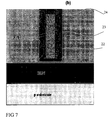
- Another aspect provides a method of manufacturing a transistor having the step of forming a trench in a first layer, filling the trench, forming a second layer on either side of the trench with lateral overgrowth over the trench, and forming a main electrode such as a drain or source region in the second layer so as to overlap the trench.
- the chip area taken up by the device can be reduced for a given size of main electrode region, e.g. drain or source region.
- main electrode region e.g. drain or source region.
- An additional feature is the step of forming a conductive element in the trench, insulated from the first layer by an insulating layer on a sidewall of the trench, a main electrode region, e.g. source or drain region extending over the insulating layer.
- Another such additional feature is forming a top layer to seal a top of the conductive element in the trench, the top layer being resistant to growth of the second layer. This can help maintain a gap above the trench to enable a contact to be made without needing a separate mask and etching step to open a gap in the second layer.
- Another such additional feature is forming an insulated spacer at the sides of the second layer over the trench. This can enable the conductive element in the trench and any contact coupled to it, to be insulated from the main electrode regions, e.g. source or drain region, so that they can be set at different potentials.
- Another such additional step is removing the top layer where it is not covered by the insulated spacer. This also enables a contact to be made to the conductive element in the trench.
- Another such additional feature is forming a control electrode structure such as a gate structure after forming the trench.
- Another aspect is a transistor having corresponding features.
- Another such additional feature is the transistor having a drift region in the first layer.
- transistor being a vertical MOS device having a buried drain or source below the first layer.
- Another such feature is a transistor comprising a discrete component wherein a drain electrode is connected at the backside of the component, e.g. at the backside of a wafer.
- An additional feature of some embodiments is the transistor being a power transistor having multiple cells, each cell having a trench. Any of the additional features can be combined together and combined with any of the aspects. Other advantages will be apparent to those skilled in the art, especially over other prior art. Numerous variations and modifications can be made without departing from the claims of the present invention. Therefore, it should be clearly understood that the form of the present invention is illustrative only and is not intended to limit the scope of the present invention.
- a self-aligned method of fabrication is proposed to align the trenches of a trench power device to a control electrode, e.g. a gate.
- a method to reduce the surface area necessary to contact the trenches is also proposed.
- the present invention may be applied to a variety of semiconductor devices such as a MOSFET, a bipolar transistor, for example a high voltage diode.
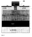
- Fig 1 illustrates a MOSFET 100, known from US 2003/0006453 . Like a conventional MOSFET, it is formed on a heavily doped n+ semiconductor substrate 102.
- the substrate may be a semiconductor wafer as is know to the skilled person. Typically the substrate will be a silicon substrate but the present invention is not limited thereto.
- the term "substrate” may include any underlying material or materials that may be used, or upon which a device, a circuit or an epitaxial layer may be formed. In other alternative embodiments, this "substrate" may include a semiconductor substrate such as e.g.
- the "substrate” may include for example, an insulating layer such as a SiO 2 or a Si 3 N 4 layer in addition to a semiconductor substrate portion.
- substrate also includes silicon-on-glass, silicon-on sapphire substrates.
- substrate is thus used to define generally the elements for layers that underlie a layer or portions of interest.
- the "substrate” may be any other base on which a layer is formed, for example a glass or metal layer.
- a more lightly doped epitaxial layer defining drift region 104 is grown on substrate 102. At the top of region 104, p-type body regions 108 are formed. n+ source regions 110 are formed within body regions 108. A gate 106 is formed atop the epitaxial layer across the p-body regions to reach source regions 110, and is insulated therefrom by an oxide layer 112. Metal contacts 114 and 116 are formed for electrical interconnection source regions 110 and substrate 102 to act as source and drain contacts, respectively. Additionally, MOSFET 100 includes sidewall metal-thick-oxide (MTO) dielectric columns 118. Each of dielectric columns 118 extends vertically at the opposite edges of n drift region 104. As such, drift region 104 resembles a column having width 2w.
- MTO metal-thick-oxide
- each dielectric column 118 is adjacent to n drift region 104 of MOSFET 100.
- the opposite edge of each column 118 is bounded by a vertically extending conductive region 120.
- Each conductive region 120 is formed of a p+/n+ poly-silicon semiconductor. As well, conductive regions 120 are electrically connected to source metal contact 114.
- the voltage across each column 118 deposits a charge at the edge of each column 118.
- This charge exerts an electric field on drift region 104 that depletes free carriers in the n column of the drift region 104 laterally. That is, free carriers are redistributed within drift region 104.
- the sidewall oxide is thermally grown to obtain the highest breakdown quality, or if any other dielectric material is chosen to replace the oxide, it should have a breakdown field strength equal to or greater than that of the thermal oxide.
- the dielectric thickness can be controlled.
- the thickness of the bottom oxide d ox can be chosen to be the same as or preferably greater than oxide thickness t ox .
- the doping in the drift region 104 can be raised to a value much higher than that permissible in conventional MOSFETs, thus improving the specific on-resistance to breakdown voltage relationship curve for silicon MOSFET 100.
- no precise matching of doping is needed in MOSFET 100.
- MOSFET 100 can be manufactured more easily and precisely than known charge compensation structures that require the difficult task of precise doping control and multiple epitaxial growth.
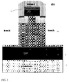
- the second embodiment described below elaborates on the fabrication of the trenches and how the filler material is contacted.
- the proposed method uses a lateral overgrowth of an epitaxial layer (see figure 8 in particular). It can further reduce the device area for the same R ON .
- the final structure has the p-well isolated from the trench polysilicon by an oxide layer.
- the trench polysilicon can be put at a different potential, improving the device performance.
- the trench is partially under the p-well, thus reducing the device area.
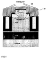
- manufacturing a power transistor involves forming a control electrode structure such as a gate structure on a first layer, forming a trench in the first layer, self aligned with the gate structure, and forming part of the transistor in the trench.
- a control electrode structure such as a gate structure on a first layer
- the spacer and gate can be used as a mask when forming the trench, to allow space for a source region next to the gate.
- the self-aligning rather than forming the gate after the trench means the alignment is more accurate, allowing size reduction.
- Another aspect involves forming a trench in a first layer, filling the trench, forming a second layer on either side of the trench with lateral overgrowth over the trench, and forming a source region in the second layer to overlap the trench. This overlap can enable the chip area to be reduced.
Landscapes
- Electrodes Of Semiconductors (AREA)
- Insulated Gate Type Field-Effect Transistor (AREA)
- Thin Film Transistor (AREA)
- Element Separation (AREA)
- Exposure Of Semiconductors, Excluding Electron Or Ion Beam Exposure (AREA)
Applications Claiming Priority (1)
| Application Number | Priority Date | Filing Date | Title |
|---|---|---|---|
| GBGB0508407.4A GB0508407D0 (en) | 2005-04-26 | 2005-04-26 | Alignment of trench for MOS |
Publications (3)
| Publication Number | Publication Date |
|---|---|
| EP1717865A2 true EP1717865A2 (de) | 2006-11-02 |
| EP1717865A3 EP1717865A3 (de) | 2007-08-08 |
| EP1717865B1 EP1717865B1 (de) | 2011-06-08 |
Family
ID=34640136
Family Applications (1)
| Application Number | Title | Priority Date | Filing Date |
|---|---|---|---|
| EP06006084A Expired - Lifetime EP1717865B1 (de) | 2005-04-26 | 2006-03-24 | Verfahren zur Herstellung eines Transistors |
Country Status (4)
| Country | Link |
|---|---|
| US (2) | US7608510B2 (de) |
| EP (1) | EP1717865B1 (de) |
| AT (1) | ATE512460T1 (de) |
| GB (1) | GB0508407D0 (de) |
Cited By (2)
| Publication number | Priority date | Publication date | Assignee | Title |
|---|---|---|---|---|
| CN109427883A (zh) * | 2017-08-23 | 2019-03-05 | 深圳市敦为技术有限公司 | 一种新型氧化硅层辅助耗尽超结结构的制造方法 |
| CN118658885A (zh) * | 2024-08-20 | 2024-09-17 | 深圳市港祥辉电子有限公司 | 一种增强型沟槽栅氧化镓vdmos器件及其制备方法 |
Families Citing this family (17)
| Publication number | Priority date | Publication date | Assignee | Title |
|---|---|---|---|---|
| US8580651B2 (en) * | 2007-04-23 | 2013-11-12 | Icemos Technology Ltd. | Methods for manufacturing a trench type semiconductor device having a thermally sensitive refill material |
| US8445913B2 (en) | 2007-10-30 | 2013-05-21 | Spansion Llc | Metal-insulator-metal (MIM) device and method of formation thereof |
| US7846821B2 (en) | 2008-02-13 | 2010-12-07 | Icemos Technology Ltd. | Multi-angle rotation for ion implantation of trenches in superjunction devices |
| TWI385802B (zh) * | 2008-09-08 | 2013-02-11 | Niko Semiconductor Co Ltd | 高壓金氧半導體元件及其製作方法 |
| US20120273916A1 (en) | 2011-04-27 | 2012-11-01 | Yedinak Joseph A | Superjunction Structures for Power Devices and Methods of Manufacture |
| US8084811B2 (en) * | 2009-10-08 | 2011-12-27 | Monolithic Power Systems, Inc. | Power devices with super junctions and associated methods manufacturing |
| US8786010B2 (en) | 2011-04-27 | 2014-07-22 | Fairchild Semiconductor Corporation | Superjunction structures for power devices and methods of manufacture |
| US8836028B2 (en) | 2011-04-27 | 2014-09-16 | Fairchild Semiconductor Corporation | Superjunction structures for power devices and methods of manufacture |
| US8772868B2 (en) | 2011-04-27 | 2014-07-08 | Fairchild Semiconductor Corporation | Superjunction structures for power devices and methods of manufacture |
| US8673700B2 (en) * | 2011-04-27 | 2014-03-18 | Fairchild Semiconductor Corporation | Superjunction structures for power devices and methods of manufacture |
| US8901641B2 (en) * | 2012-02-01 | 2014-12-02 | Vanguard International Semiconductor Corporation | Semiconductor device with super junction structure and method for fabricating the same |
| US9312382B2 (en) * | 2014-07-22 | 2016-04-12 | Empire Technology Development Llc | High voltage transistor device with reduced characteristic on resistance |
| CN106158975A (zh) * | 2016-08-30 | 2016-11-23 | 扬州扬杰电子科技股份有限公司 | 一种带屏蔽电极的功率mosfet元胞及其加工工艺 |
| EP3475690A4 (de) * | 2016-10-05 | 2019-05-08 | Hewlett-Packard Development Company, L.P. | Isolierte sensoren |
| DE102017128241B3 (de) * | 2017-11-29 | 2019-02-07 | Infineon Technologies Austria Ag | Layout für einen Nadelzellengraben-MOSFET und Verfahren zu dessen Verarbeitung |
| US20190386124A1 (en) * | 2018-06-13 | 2019-12-19 | Purdue Research Foundation | Mos devices with increased short circuit robustness |
| EP4092724A1 (de) * | 2021-05-21 | 2022-11-23 | Infineon Technologies Austria AG | Halbleiterchip mit vertikaler leistungstransistorvorrichtung |
Family Cites Families (24)
| Publication number | Priority date | Publication date | Assignee | Title |
|---|---|---|---|---|
| US4554570A (en) * | 1982-06-24 | 1985-11-19 | Rca Corporation | Vertically integrated IGFET device |
| CN1019720B (zh) * | 1991-03-19 | 1992-12-30 | 电子科技大学 | 半导体功率器件 |
| US5340754A (en) * | 1992-09-02 | 1994-08-23 | Motorla, Inc. | Method for forming a transistor having a dynamic connection between a substrate and a channel region |
| US5554870A (en) * | 1994-02-04 | 1996-09-10 | Motorola, Inc. | Integrated circuit having both vertical and horizontal devices and process for making the same |
| JPH11251581A (ja) | 1998-03-02 | 1999-09-17 | Toshiba Corp | 半導体装置およびその製造方法 |
| US5981350A (en) * | 1998-05-29 | 1999-11-09 | Micron Technology, Inc. | Method for forming high capacitance memory cells |
| JP2000208757A (ja) * | 1999-01-08 | 2000-07-28 | Nippon Telegr & Teleph Corp <Ntt> | 絶縁ゲ―ト型半導体装置及びその製法 |
| JP3971062B2 (ja) * | 1999-07-29 | 2007-09-05 | 株式会社東芝 | 高耐圧半導体装置 |
| JP3356162B2 (ja) * | 1999-10-19 | 2002-12-09 | 株式会社デンソー | 半導体装置及びその製造方法 |
| US6475864B1 (en) | 1999-10-21 | 2002-11-05 | Fuji Electric Co., Ltd. | Method of manufacturing a super-junction semiconductor device with an conductivity type layer |
| US6326272B1 (en) * | 1999-11-18 | 2001-12-04 | Chartered Semiconductor Manufacturing Ltd. | Method for forming self-aligned elevated transistor |
| US6541343B1 (en) * | 1999-12-30 | 2003-04-01 | Intel Corporation | Methods of making field effect transistor structure with partially isolated source/drain junctions |
| KR20010077099A (ko) * | 2000-01-31 | 2001-08-17 | 윤종용 | 자기 정렬된 웰 바이어스 영역을 갖는 모스 트랜지스터 및그 제조방법 |
| TW469635B (en) * | 2000-05-16 | 2001-12-21 | Nanya Technology Corp | Fabrication method of semiconductor memory cell transistor |
| JP2001332635A (ja) | 2000-05-19 | 2001-11-30 | Nec Corp | 不揮発性半導体記憶装置及びその製造方法 |
| US6853033B2 (en) * | 2001-06-05 | 2005-02-08 | National University Of Singapore | Power MOSFET having enhanced breakdown voltage |
| US6555873B2 (en) * | 2001-09-07 | 2003-04-29 | Power Integrations, Inc. | High-voltage lateral transistor with a multi-layered extended drain structure |
| US6635544B2 (en) * | 2001-09-07 | 2003-10-21 | Power Intergrations, Inc. | Method of fabricating a high-voltage transistor with a multi-layered extended drain structure |
| JP4322453B2 (ja) * | 2001-09-27 | 2009-09-02 | 株式会社東芝 | 半導体装置およびその製造方法 |
| US6750524B2 (en) * | 2002-05-14 | 2004-06-15 | Motorola Freescale Semiconductor | Trench MOS RESURF super-junction devices |
| KR100481209B1 (ko) * | 2002-10-01 | 2005-04-08 | 삼성전자주식회사 | 다중 채널을 갖는 모스 트랜지스터 및 그 제조방법 |
| US6743684B2 (en) * | 2002-10-11 | 2004-06-01 | Texas Instruments Incorporated | Method to produce localized halo for MOS transistor |
| US7238581B2 (en) * | 2004-08-05 | 2007-07-03 | Chartered Semiconductor Manufacturing Ltd. | Method of manufacturing a semiconductor device with a strained channel |
| US7659189B2 (en) * | 2007-03-16 | 2010-02-09 | United Microelectronics Corp. | Method for forming fully silicided gate electrode in a semiconductor device |
-
2005
- 2005-04-26 GB GBGB0508407.4A patent/GB0508407D0/en not_active Ceased
-
2006
- 2006-03-24 EP EP06006084A patent/EP1717865B1/de not_active Expired - Lifetime
- 2006-03-24 AT AT06006084T patent/ATE512460T1/de not_active IP Right Cessation
- 2006-04-24 US US11/408,924 patent/US7608510B2/en active Active
-
2009
- 2009-09-15 US US12/560,025 patent/US7989886B2/en active Active
Cited By (2)
| Publication number | Priority date | Publication date | Assignee | Title |
|---|---|---|---|---|
| CN109427883A (zh) * | 2017-08-23 | 2019-03-05 | 深圳市敦为技术有限公司 | 一种新型氧化硅层辅助耗尽超结结构的制造方法 |
| CN118658885A (zh) * | 2024-08-20 | 2024-09-17 | 深圳市港祥辉电子有限公司 | 一种增强型沟槽栅氧化镓vdmos器件及其制备方法 |
Also Published As
| Publication number | Publication date |
|---|---|
| EP1717865A3 (de) | 2007-08-08 |
| US20100065908A1 (en) | 2010-03-18 |
| US7608510B2 (en) | 2009-10-27 |
| ATE512460T1 (de) | 2011-06-15 |
| GB0508407D0 (en) | 2005-06-01 |
| US20060249786A1 (en) | 2006-11-09 |
| US7989886B2 (en) | 2011-08-02 |
| EP1717865B1 (de) | 2011-06-08 |
Similar Documents
| Publication | Publication Date | Title |
|---|---|---|
| US7989886B2 (en) | Alignment of trench for MOS | |
| US9865678B2 (en) | High voltage field balance metal oxide field effect transistor (FBM) | |
| US7183610B2 (en) | Super trench MOSFET including buried source electrode and method of fabricating the same | |
| US7679146B2 (en) | Semiconductor device having sub-surface trench charge compensation regions | |
| CN100524809C (zh) | 场效应晶体管半导体器件 | |
| CN1822389B (zh) | 具有深槽电荷补偿区的半导体器件及方法 | |
| CN100565917C (zh) | 半导体器件边缘终端结构及方法 | |
| US7411266B2 (en) | Semiconductor device having trench charge compensation regions and method | |
| US7602014B2 (en) | Superjunction power MOSFET | |
| US7989293B2 (en) | Trench device structure and fabrication | |
| CN100576563C (zh) | 超结半导体器件结构和方法 | |
| US20050167695A1 (en) | Semiconductor device containing dielectrically isolated pn junction for enhanced breakdown characteristics | |
| US20120094457A1 (en) | Sti-aligned ldmos drift implant to enhance manufacturability while optimizing rdson and safe operating area | |
| US20120261746A1 (en) | Double-Trench Vertical Devices and Methods with Self-Alignment Between Gate and Body Contact | |
| US8889518B2 (en) | LDMOS transistor with asymmetric spacer as gate | |
| US20120098056A1 (en) | Trench device structure and fabrication | |
| HK1114947B (en) | Semiconductor device having trench charge compensation regions and method | |
| HK1103168A1 (en) | Semiconductor structure with improved on resistance and breakdown voltage performance | |
| WO2010098742A1 (en) | Trench device structure and fabrication | |
| HK1103168B (en) | Semiconductor structure with improved on resistance and breakdown voltage performance | |
| HK1103167A1 (en) | Semiconductor structure with improved on resistance and breakdown voltage performance | |
| HK1103167B (en) | Semiconductor structure with improved on resistance and breakdown voltage performance |
Legal Events
| Date | Code | Title | Description |
|---|---|---|---|
| PUAI | Public reference made under article 153(3) epc to a published international application that has entered the european phase |
Free format text: ORIGINAL CODE: 0009012 |
|
| AK | Designated contracting states |
Kind code of ref document: A2 Designated state(s): AT BE BG CH CY CZ DE DK EE ES FI FR GB GR HU IE IS IT LI LT LU LV MC NL PL PT RO SE SI SK TR |
|
| AX | Request for extension of the european patent |
Extension state: AL BA HR MK YU |
|
| PUAL | Search report despatched |
Free format text: ORIGINAL CODE: 0009013 |
|
| AK | Designated contracting states |
Kind code of ref document: A3 Designated state(s): AT BE BG CH CY CZ DE DK EE ES FI FR GB GR HU IE IS IT LI LT LU LV MC NL PL PT RO SE SI SK TR |
|
| AX | Request for extension of the european patent |
Extension state: AL BA HR MK YU |
|
| 17P | Request for examination filed |
Effective date: 20071026 |
|
| AKX | Designation fees paid |
Designated state(s): AT BE BG CH CY CZ DE DK EE ES FI FR GB GR HU IE IS IT LI LT LU LV MC NL PL PT RO SE SI SK TR |
|
| RAP1 | Party data changed (applicant data changed or rights of an application transferred) |
Owner name: SEMICONDUCTOR COMPONENTS INDUSTRIES, LLC |
|
| GRAJ | Information related to disapproval of communication of intention to grant by the applicant or resumption of examination proceedings by the epo deleted |
Free format text: ORIGINAL CODE: EPIDOSDIGR1 |
|
| GRAP | Despatch of communication of intention to grant a patent |
Free format text: ORIGINAL CODE: EPIDOSNIGR1 |
|
| GRAP | Despatch of communication of intention to grant a patent |
Free format text: ORIGINAL CODE: EPIDOSNIGR1 |
|
| RIC1 | Information provided on ipc code assigned before grant |
Ipc: H01L 29/417 20060101ALN20101026BHEP Ipc: H01L 21/336 20060101AFI20101026BHEP Ipc: H01L 29/41 20060101ALI20101026BHEP Ipc: H01L 29/78 20060101ALI20101026BHEP |
|
| RTI1 | Title (correction) |
Free format text: METHOD OF MAKING A TRANSISTOR |
|
| GRAS | Grant fee paid |
Free format text: ORIGINAL CODE: EPIDOSNIGR3 |
|
| GRAA | (expected) grant |
Free format text: ORIGINAL CODE: 0009210 |
|
| AK | Designated contracting states |
Kind code of ref document: B1 Designated state(s): AT BE BG CH CY CZ DE DK EE ES FI FR GB GR HU IE IS IT LI LT LU LV MC NL PL PT RO SE SI SK TR |
|
| REG | Reference to a national code |
Ref country code: GB Ref legal event code: FG4D |
|
| REG | Reference to a national code |
Ref country code: CH Ref legal event code: EP |
|
| REG | Reference to a national code |
Ref country code: IE Ref legal event code: FG4D |
|
| REG | Reference to a national code |
Ref country code: DE Ref legal event code: R096 Ref document number: 602006022326 Country of ref document: DE Effective date: 20110721 |
|
| REG | Reference to a national code |
Ref country code: NL Ref legal event code: VDEP Effective date: 20110608 |
|
| PG25 | Lapsed in a contracting state [announced via postgrant information from national office to epo] |
Ref country code: SE Free format text: LAPSE BECAUSE OF FAILURE TO SUBMIT A TRANSLATION OF THE DESCRIPTION OR TO PAY THE FEE WITHIN THE PRESCRIBED TIME-LIMIT Effective date: 20110608 Ref country code: LT Free format text: LAPSE BECAUSE OF FAILURE TO SUBMIT A TRANSLATION OF THE DESCRIPTION OR TO PAY THE FEE WITHIN THE PRESCRIBED TIME-LIMIT Effective date: 20110608 |
|
| PG25 | Lapsed in a contracting state [announced via postgrant information from national office to epo] |
Ref country code: ES Free format text: LAPSE BECAUSE OF FAILURE TO SUBMIT A TRANSLATION OF THE DESCRIPTION OR TO PAY THE FEE WITHIN THE PRESCRIBED TIME-LIMIT Effective date: 20110919 Ref country code: AT Free format text: LAPSE BECAUSE OF FAILURE TO SUBMIT A TRANSLATION OF THE DESCRIPTION OR TO PAY THE FEE WITHIN THE PRESCRIBED TIME-LIMIT Effective date: 20110608 Ref country code: CY Free format text: LAPSE BECAUSE OF FAILURE TO SUBMIT A TRANSLATION OF THE DESCRIPTION OR TO PAY THE FEE WITHIN THE PRESCRIBED TIME-LIMIT Effective date: 20110608 Ref country code: SI Free format text: LAPSE BECAUSE OF FAILURE TO SUBMIT A TRANSLATION OF THE DESCRIPTION OR TO PAY THE FEE WITHIN THE PRESCRIBED TIME-LIMIT Effective date: 20110608 Ref country code: GR Free format text: LAPSE BECAUSE OF FAILURE TO SUBMIT A TRANSLATION OF THE DESCRIPTION OR TO PAY THE FEE WITHIN THE PRESCRIBED TIME-LIMIT Effective date: 20110909 Ref country code: LV Free format text: LAPSE BECAUSE OF FAILURE TO SUBMIT A TRANSLATION OF THE DESCRIPTION OR TO PAY THE FEE WITHIN THE PRESCRIBED TIME-LIMIT Effective date: 20110608 Ref country code: FI Free format text: LAPSE BECAUSE OF FAILURE TO SUBMIT A TRANSLATION OF THE DESCRIPTION OR TO PAY THE FEE WITHIN THE PRESCRIBED TIME-LIMIT Effective date: 20110608 |
|
| PG25 | Lapsed in a contracting state [announced via postgrant information from national office to epo] |
Ref country code: BE Free format text: LAPSE BECAUSE OF FAILURE TO SUBMIT A TRANSLATION OF THE DESCRIPTION OR TO PAY THE FEE WITHIN THE PRESCRIBED TIME-LIMIT Effective date: 20110608 Ref country code: NL Free format text: LAPSE BECAUSE OF FAILURE TO SUBMIT A TRANSLATION OF THE DESCRIPTION OR TO PAY THE FEE WITHIN THE PRESCRIBED TIME-LIMIT Effective date: 20110608 |
|
| PG25 | Lapsed in a contracting state [announced via postgrant information from national office to epo] |
Ref country code: PT Free format text: LAPSE BECAUSE OF FAILURE TO SUBMIT A TRANSLATION OF THE DESCRIPTION OR TO PAY THE FEE WITHIN THE PRESCRIBED TIME-LIMIT Effective date: 20111010 Ref country code: EE Free format text: LAPSE BECAUSE OF FAILURE TO SUBMIT A TRANSLATION OF THE DESCRIPTION OR TO PAY THE FEE WITHIN THE PRESCRIBED TIME-LIMIT Effective date: 20110608 Ref country code: CZ Free format text: LAPSE BECAUSE OF FAILURE TO SUBMIT A TRANSLATION OF THE DESCRIPTION OR TO PAY THE FEE WITHIN THE PRESCRIBED TIME-LIMIT Effective date: 20110608 Ref country code: IS Free format text: LAPSE BECAUSE OF FAILURE TO SUBMIT A TRANSLATION OF THE DESCRIPTION OR TO PAY THE FEE WITHIN THE PRESCRIBED TIME-LIMIT Effective date: 20111008 |
|
| PG25 | Lapsed in a contracting state [announced via postgrant information from national office to epo] |
Ref country code: PL Free format text: LAPSE BECAUSE OF FAILURE TO SUBMIT A TRANSLATION OF THE DESCRIPTION OR TO PAY THE FEE WITHIN THE PRESCRIBED TIME-LIMIT Effective date: 20110608 Ref country code: RO Free format text: LAPSE BECAUSE OF FAILURE TO SUBMIT A TRANSLATION OF THE DESCRIPTION OR TO PAY THE FEE WITHIN THE PRESCRIBED TIME-LIMIT Effective date: 20110608 Ref country code: SK Free format text: LAPSE BECAUSE OF FAILURE TO SUBMIT A TRANSLATION OF THE DESCRIPTION OR TO PAY THE FEE WITHIN THE PRESCRIBED TIME-LIMIT Effective date: 20110608 |
|
| PLBE | No opposition filed within time limit |
Free format text: ORIGINAL CODE: 0009261 |
|
| STAA | Information on the status of an ep patent application or granted ep patent |
Free format text: STATUS: NO OPPOSITION FILED WITHIN TIME LIMIT |
|
| 26N | No opposition filed |
Effective date: 20120309 |
|
| PG25 | Lapsed in a contracting state [announced via postgrant information from national office to epo] |
Ref country code: DK Free format text: LAPSE BECAUSE OF FAILURE TO SUBMIT A TRANSLATION OF THE DESCRIPTION OR TO PAY THE FEE WITHIN THE PRESCRIBED TIME-LIMIT Effective date: 20110608 |
|
| REG | Reference to a national code |
Ref country code: DE Ref legal event code: R097 Ref document number: 602006022326 Country of ref document: DE Effective date: 20120309 |
|
| PG25 | Lapsed in a contracting state [announced via postgrant information from national office to epo] |
Ref country code: MC Free format text: LAPSE BECAUSE OF NON-PAYMENT OF DUE FEES Effective date: 20120331 |
|
| REG | Reference to a national code |
Ref country code: CH Ref legal event code: PL |
|
| GBPC | Gb: european patent ceased through non-payment of renewal fee |
Effective date: 20120324 |
|
| REG | Reference to a national code |
Ref country code: IE Ref legal event code: MM4A |
|
| PG25 | Lapsed in a contracting state [announced via postgrant information from national office to epo] |
Ref country code: LI Free format text: LAPSE BECAUSE OF NON-PAYMENT OF DUE FEES Effective date: 20120331 Ref country code: IE Free format text: LAPSE BECAUSE OF NON-PAYMENT OF DUE FEES Effective date: 20120324 Ref country code: CH Free format text: LAPSE BECAUSE OF NON-PAYMENT OF DUE FEES Effective date: 20120331 Ref country code: GB Free format text: LAPSE BECAUSE OF NON-PAYMENT OF DUE FEES Effective date: 20120324 |
|
| PG25 | Lapsed in a contracting state [announced via postgrant information from national office to epo] |
Ref country code: BG Free format text: LAPSE BECAUSE OF FAILURE TO SUBMIT A TRANSLATION OF THE DESCRIPTION OR TO PAY THE FEE WITHIN THE PRESCRIBED TIME-LIMIT Effective date: 20110908 |
|
| PG25 | Lapsed in a contracting state [announced via postgrant information from national office to epo] |
Ref country code: TR Free format text: LAPSE BECAUSE OF FAILURE TO SUBMIT A TRANSLATION OF THE DESCRIPTION OR TO PAY THE FEE WITHIN THE PRESCRIBED TIME-LIMIT Effective date: 20110608 |
|
| PG25 | Lapsed in a contracting state [announced via postgrant information from national office to epo] |
Ref country code: LU Free format text: LAPSE BECAUSE OF NON-PAYMENT OF DUE FEES Effective date: 20120324 |
|
| PG25 | Lapsed in a contracting state [announced via postgrant information from national office to epo] |
Ref country code: HU Free format text: LAPSE BECAUSE OF FAILURE TO SUBMIT A TRANSLATION OF THE DESCRIPTION OR TO PAY THE FEE WITHIN THE PRESCRIBED TIME-LIMIT Effective date: 20060324 |
|
| REG | Reference to a national code |
Ref country code: FR Ref legal event code: PLFP Year of fee payment: 11 |
|
| REG | Reference to a national code |
Ref country code: FR Ref legal event code: PLFP Year of fee payment: 12 |
|
| REG | Reference to a national code |
Ref country code: FR Ref legal event code: PLFP Year of fee payment: 13 |
|
| PGFP | Annual fee paid to national office [announced via postgrant information from national office to epo] |
Ref country code: IT Payment date: 20200218 Year of fee payment: 15 |
|
| PGFP | Annual fee paid to national office [announced via postgrant information from national office to epo] |
Ref country code: FR Payment date: 20200220 Year of fee payment: 15 |
|
| PG25 | Lapsed in a contracting state [announced via postgrant information from national office to epo] |
Ref country code: FR Free format text: LAPSE BECAUSE OF NON-PAYMENT OF DUE FEES Effective date: 20210331 |
|
| PG25 | Lapsed in a contracting state [announced via postgrant information from national office to epo] |
Ref country code: IT Free format text: LAPSE BECAUSE OF NON-PAYMENT OF DUE FEES Effective date: 20210324 |
|
| P01 | Opt-out of the competence of the unified patent court (upc) registered |
Effective date: 20230519 |
|
| PGFP | Annual fee paid to national office [announced via postgrant information from national office to epo] |
Ref country code: DE Payment date: 20240220 Year of fee payment: 19 |
|
| REG | Reference to a national code |
Ref country code: DE Ref legal event code: R079 Ref document number: 602006022326 Country of ref document: DE Free format text: PREVIOUS MAIN CLASS: H01L0029780000 Ipc: H10D0030600000 |
|
| REG | Reference to a national code |
Ref country code: DE Ref legal event code: R119 Ref document number: 602006022326 Country of ref document: DE |
|
| PG25 | Lapsed in a contracting state [announced via postgrant information from national office to epo] |
Ref country code: DE Free format text: LAPSE BECAUSE OF NON-PAYMENT OF DUE FEES Effective date: 20251001 |