EP1722483A2 - Circuit de commutation - Google Patents
Circuit de commutation Download PDFInfo
- Publication number
- EP1722483A2 EP1722483A2 EP06111599A EP06111599A EP1722483A2 EP 1722483 A2 EP1722483 A2 EP 1722483A2 EP 06111599 A EP06111599 A EP 06111599A EP 06111599 A EP06111599 A EP 06111599A EP 1722483 A2 EP1722483 A2 EP 1722483A2
- Authority
- EP
- European Patent Office
- Prior art keywords
- input terminal
- frequency
- diode
- trap
- terminal
- Prior art date
- Legal status (The legal status is an assumption and is not a legal conclusion. Google has not performed a legal analysis and makes no representation as to the accuracy of the status listed.)
- Withdrawn
Links
- 238000002955 isolation Methods 0.000 description 12
- 230000005540 biological transmission Effects 0.000 description 5
- 239000003990 capacitor Substances 0.000 description 5
- 238000010586 diagram Methods 0.000 description 3
- 238000011144 upstream manufacturing Methods 0.000 description 3
- 230000010355 oscillation Effects 0.000 description 2
- 230000002238 attenuated effect Effects 0.000 description 1
- 238000006243 chemical reaction Methods 0.000 description 1
- 238000010276 construction Methods 0.000 description 1
Images

Classifications
-
- H—ELECTRICITY
- H04—ELECTRIC COMMUNICATION TECHNIQUE
- H04B—TRANSMISSION
- H04B1/00—Details of transmission systems, not covered by a single one of groups H04B3/00 - H04B13/00; Details of transmission systems not characterised by the medium used for transmission
- H04B1/38—Transceivers, i.e. devices in which transmitter and receiver form a structural unit and in which at least one part is used for functions of transmitting and receiving
- H04B1/40—Circuits
- H04B1/44—Transmit/receive switching
- H04B1/48—Transmit/receive switching in circuits for connecting transmitter and receiver to a common transmission path, e.g. by energy of transmitter
-
- H—ELECTRICITY
- H03—ELECTRONIC CIRCUITRY
- H03K—PULSE TECHNIQUE
- H03K17/00—Electronic switching or gating, i.e. not by contact-making and –breaking
- H03K17/51—Electronic switching or gating, i.e. not by contact-making and –breaking characterised by the components used
- H03K17/74—Electronic switching or gating, i.e. not by contact-making and –breaking characterised by the components used by the use, as active elements, of diodes
- H03K17/76—Switching arrangements with several input- or output-terminals, e.g. multiplexers, distributors
-
- H—ELECTRICITY
- H03—ELECTRONIC CIRCUITRY
- H03J—TUNING RESONANT CIRCUITS; SELECTING RESONANT CIRCUITS
- H03J5/00—Discontinuous tuning; Selecting predetermined frequencies; Selecting frequency bands with or without continuous tuning in one or more of the bands, e.g. push-button tuning, turret tuner
- H03J5/24—Discontinuous tuning; Selecting predetermined frequencies; Selecting frequency bands with or without continuous tuning in one or more of the bands, e.g. push-button tuning, turret tuner with a number of separate pretuned tuning circuits or separate tuning elements selectively brought into circuit, e.g. for waveband selection or for television channel selection
- H03J5/246—Discontinuous tuning; Selecting predetermined frequencies; Selecting frequency bands with or without continuous tuning in one or more of the bands, e.g. push-button tuning, turret tuner with a number of separate pretuned tuning circuits or separate tuning elements selectively brought into circuit, e.g. for waveband selection or for television channel selection using electronic means
Definitions
- the present invention relates to a single pole double throw (SPDT) type switch circuit suitable for use in an outdoor converter (BS converter) to receive satellite broadcast signal.
- SPDT single pole double throw
- a conventional BS converter using a single pole double throw type switch circuit will be described with reference to Fig. 4.
- Left turning satellite broadcasting signals of a 12 GHz band input to a first input terminal 1 are input to a first mixer 4 through a first low-noise amplifier 2 and a first band pass filter 3.
- Local oscillation signals are transmitted to the first mixer 4 from a local oscillator 5.
- a first intermediate frequency signal of about 1 GHz output from the first mixer 4 is input to a first resistance divider 31 through a first intermediate frequency head amplifier 6.
- right turning broadcasting signals of a 12 GHz band input to a second input terminal 7 are input to a second mixer 10 through a second low-noise amplifier 8 and a second band pass filter 9. Local oscillation signals are transmitted to the second mixer 10 as well.
- a second intermediate frequency signal of about 1 GHz output from the second mixer 10 is input to a second resistance divider 32 through a second intermediate frequency head amplifier 11.
- One of one side of the first intermediate frequency signal divided by the first resistance divider 31 and one side of the second intermediate frequency signal divided by the second resistance divider 32 is selected by a first converting switch 33, and is then output to a first output terminal 14 through a first intermediate frequency output amplifier 12.
- One of the other side of the first intermediate frequency signal divided by the first resistance divider 31 and the other side of the second intermediate frequency signal divided by the second resistance divider 32 is selected by a second converting switch 34, and is then output to a second output terminal 15 through a second intermediate frequency output amplifier 13 (For example, see JP-A-2004-235801 (Fig. 1)).
- Each of the first converting switch 33 and the second converting switch 34 includes two pin diodes. When one diode is turned on, the other diode is turned off.
- the converting switch has the construction in which one of the two input terminals is connected to an output terminal. Therefore, when one input terminal is connected to the output terminal, the other input terminal is opened. Thus, a circuit connected to an upstream end of an open input terminal is opened, and signals of the circuit are prone to intrude into an output terminal, whereby isolation between the two input terminals deteriorates.
- a switch circuit includes: a first input terminal; a second input terminal; an output terminal which is selectively connected to the first input terminal or the second input terminal; and terminators for terminating the first input terminal or the second input terminal.
- the second input terminal is terminated by the terminator.
- the first input terminal is terminated by the terminator.
- each of the terminators is formed of a series circuit including a diode and a resistor, and the series circuits are connected between the first input terminal and a ground and between the second input terminal and a ground, respectively. Further, the diodes of the two series circuits are selectively turned on.
- the impedances of the series circuits when the diodes are turned on are set to the same as impedances of circuits that are connected to the first input terminal and the second input terminal, respectively.
- each of the terminators is composed of a trap circuit whose trap frequency is converted at a first frequency or a second frequency higher than the first frequency, and the trap circuits are connected between the first input terminal and a ground and between the second input terminal and a ground, respectively.
- the trap circuit connects the first input terminal the output terminal, the first frequency is trapped by the trap circuit that is connected to the first input terminal, and the second frequency is trapped by the trap circuit that is connected to the second input terminal.
- the trap circuit connects the second input terminal and the output terminal, the first frequency is trapped by the trap circuit that is connected to the second input terminal, and the second frequency is trapped by the trap circuit that is connected to the first input terminal.
- each of the trap circuits includes a diode, a resistor that is directly connected to the diode, a first capacitive element that is connected to the diode in parallel, and a series resonant circuit that is connected to the resistor in parallel. Further, the diodes of the two trap circuits are selectively turned on.
- the first frequency is set to be lower than the lowest frequency of the frequency band of signals that are input to the first input terminal and the second input terminal, and the second frequency is set to the vicinity of the highest frequency of the frequency band.
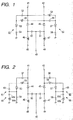
- a cathode of a first diode 44 is connected to a first input terminal 41.
- An anode of the first diode 44 is connected to a first control terminal 48 through a first choke inductor 46, and is connected to an output terminal 43 through a first DC cut capacitor 50.
- a cathode of a second diode 45 is connected to a second input terminal 42.
- An anode of the second diode 45 is connected to a second control terminal 49 through a second choke inductor 47, and is connected to the output terminal 43 through a second DC cut capacitor 51.
- the cathode of the first diode 44 is connected to an anode of a third diode 53 through a third DC cut capacitor 52, and is grounded through a first resistor 54.
- a first terminator 61 is composed of a series circuit including the third diode 53 and the first resistor 54.
- the anode of the third diode 53 is connected to the cathode of the second diode 45 through a third choke inductor 55.
- the cathode of the second diode 45 is connected to an anode of a fourth diode 57 through a fourth DC cut capacitor 56, and is grounded trough a second resistor 58.
- a second terminator 62 is composed of a series circuit including the fourth diode 57 and the second resistor 58.
- the anode of the fourth diode 57 is connected to the cathode of the first diode 44 through a fourth choke inductor 59.
- Each of the first to fourth diodes 44, 45, 53, and 57 is composed of a pin diode, and each of the first to fourth DC cut capacitors 50, 51, 52, and 56 shows low impedance for a high frequency signal. Further, each of the resistance values of the first resistor 54 and the second resistor 58 is about 500.
- Preceding ends of a first input terminal 41 and a second input terminal 42 are connected to, for example, mixers (not shown) for frequency conversion, respectively.
- Satellite broadcasting signals (intermediate frequency signals) in the range of 1 to 2.5 GHz, which are converted by the respective mixers so as to have intermediate frequencies, are input to the upstream ends.
- a right polarized intermediate frequency signal is input to the first input terminal 41, and a left polarized intermediate frequency signal is input to the second input terminal 42.
- An intermediate frequency amplifier (not shown) is connected to the output terminal 43. Further, any one of the right polarized intermediate frequency signal that is input to the first input terminal 41 and the left polarized intermediate frequency signal that is input to the second input terminal 42 is selected so as to be output to the output terminal 43.
- Fig. 2 differences from the configuration of Fig. 1 are found in the first terminator 61 and the second terminator 62, and in that the third choke inductor 55 is connected between the anode of the third diode 53 and the cathode of the first diode 44, and the fourth choke inductor 59 is connected between the anode of the fourth diode 57 and the cathode of the second diode 45.
- the rest of the configuration is the same as that of Fig. 1.
- a first capacitive element 63 having low capacitance is connected to the third diode 53 in parallel, a first series resonant circuit 64 is connected to the first resistor 54 in parallel.
- the capacitance of the first capacitive element 63 is about 0.6 pF.
- the first series resonant circuit 64 includes a second capacitive element 64a and a first inductance element 64b, the capacitance of the second capacitive element 64a is about 8.0 pF, and the inductance of the first inductance element 64b is about 4.3 nH.
- the second terminator 62 has the same configuration as the first terminator 61. That is, a third capacitive element 65 having low capacitance is connected to the fourth diode 57 in parallel, and a second series resonant circuit 66 is connected to the second resistor 58 in parallel.
- the capacitance of the third capacitive element 65 is about 0.6 pF.
- the series second resonance circuit 66 includes a fourth capacitive element 66a and a second inductance element 66b, the capacitance of the fourth capacitive element 66a is about 8.0 pF, and the inductance of the second inductance element 66b is about 4.3 nH.
- the first terminator 61 When the third diode 53 is in the ON state, the first terminator 61 represents the resonance characteristics of the first series resonant circuit 64, and the resonance frequency thereof becomes about 860 MHz. In addition, when the third diode 53 is not in the ON state, the capacitance between the terminals of the third diode 53 is about 0.4 pF, and thus the resonance frequency becomes about 2570 MHz. Therefore, the first terminator 61 and the second terminator 62 function as trap circuits in which series resonance frequency is converted into 860 MHz or 2570 MHz.
- the second diode 45 is not turned on, and the fourth diode 57 is not turned on as well, so that the second terminator 62 traps 2570 MHz and the transmission characteristics between the second input terminal 42 and the output terminal 43 becomes like B shown in Fig. 3.
- the second terminator 62 was not provided, the transmission characteristics between the second input terminal 42 and the output terminal 43 becomes like C shown in Fig. 3.
- the second terminator 62 is provided to improve isolation, even though transmission level increases and isolation deteriorates as the frequency increases.
- a switch circuit includes a first input terminal; a second input terminal; an output terminal which is selectively connected to the first input terminal or the second input terminal; and terminators for terminating the first input terminal or the second input terminal.
- the second input terminal is terminated by the terminator.
- the first input terminal is terminated by the terminator. Therefore, a signal input to the input terminal on the open side is not reflected, and thus a signal is prevented from intruding into the input terminal and the output terminal on the other side, whereby isolation is improved.
- each of the terminators is formed of a series circuit including a diode and a resistor, and the series circuits are connected between the first input terminal and a ground and between the second input terminal and a ground, respectively. Further, the diodes of the two series circuits are selectively turned on. Therefore, the input terminal on the open side can be terminated by a resistor.
- the impedances of the series circuits when the diodes are turned on are set to the same as impedances of circuits that are connected to the first input terminal and the second input terminal, respectively. Therefore, the input terminal on the open side can be terminated, in a state in which the impedances of upstream circuits connected to the input terminal on the open side are matched with each other.
- each of the terminators is composed of a trap circuit whose trap frequency is converted at a first frequency or a second frequency higher than the first frequency, and the trap circuits are connected between the first input terminal and a ground and between the second input terminal and a ground, respectively.
- the trap circuit connects the first input terminal the output terminal, the first frequency is trapped by the trap circuit that is connected to the first input terminal, and the second frequency is trapped by the trap circuit that is connected to the second input terminal.
- the trap circuit connects the second input terminal and the output terminal, the first frequency is trapped by the trap circuit that is connected to the second input terminal, and the second frequency is trapped by the trap circuit that is connected to the first input terminal. Therefore, a signal input to the input terminal on the open side can be attenuated, and signals are prevented from intruding into other input terminal and output terminal, whereby isolation is further improved. In particular, isolation at the high frequency band can be improved.
- each of the trap circuits includes a diode, a resistor that is directly connected to the diode, a first capacitive element that is connected to the diode in parallel, and a series resonant circuit that is connected to the resistor in parallel.
- the diodes of the two trap circuits are selectively turned on. Therefore, the trap frequency can be converted between two of the frequencies.
- the first frequency is set to be lower than the lowest frequency of the frequency band of signals that are input to the first input terminal and the second input terminal, and the second frequency is set to the vicinity of the highest frequency of the frequency band. Therefore, it is possible to correct the frequency characteristics of input signals at the low frequency band, and high frequency band isolation at the terminal to which signals are not input.
Landscapes
- Engineering & Computer Science (AREA)
- Computer Networks & Wireless Communication (AREA)
- Signal Processing (AREA)
- Input Circuits Of Receivers And Coupling Of Receivers And Audio Equipment (AREA)
- Electronic Switches (AREA)
- Logic Circuits (AREA)
Applications Claiming Priority (1)
| Application Number | Priority Date | Filing Date | Title |
|---|---|---|---|
| JP2005137478A JP2006319435A (ja) | 2005-05-10 | 2005-05-10 | スイッチ回路 |
Publications (2)
| Publication Number | Publication Date |
|---|---|
| EP1722483A2 true EP1722483A2 (fr) | 2006-11-15 |
| EP1722483A3 EP1722483A3 (fr) | 2007-09-05 |
Family
ID=36699033
Family Applications (1)
| Application Number | Title | Priority Date | Filing Date |
|---|---|---|---|
| EP06111599A Withdrawn EP1722483A3 (fr) | 2005-05-10 | 2006-03-23 | Circuit de commutation |
Country Status (2)
| Country | Link |
|---|---|
| EP (1) | EP1722483A3 (fr) |
| JP (1) | JP2006319435A (fr) |
Cited By (1)
| Publication number | Priority date | Publication date | Assignee | Title |
|---|---|---|---|---|
| RU2810687C1 (ru) * | 2023-08-01 | 2023-12-28 | Акционерное общество "ОКБ-Планета" | Защитное устройство СВЧ |
Families Citing this family (1)
| Publication number | Priority date | Publication date | Assignee | Title |
|---|---|---|---|---|
| JP4675943B2 (ja) * | 2007-08-24 | 2011-04-27 | Dxアンテナ株式会社 | 高周波増幅器 |
Citations (5)
| Publication number | Priority date | Publication date | Assignee | Title |
|---|---|---|---|---|
| US5327017A (en) | 1989-11-15 | 1994-07-05 | Deutsche Thomson-Brandt Gmbh | Circuit arrangement for switching of RF signals |
| EP0788185A1 (fr) | 1996-01-31 | 1997-08-06 | Matsushita Electric Industrial Co., Ltd. | Commutateur et atténuateur |
| US6351195B1 (en) | 1999-02-23 | 2002-02-26 | Murata Manufacturing Co., Ltd. | High frequency circuit device, antenna-sharing device, and communication apparatus having spaced apart ground electrodes |
| US20020105391A1 (en) | 2000-04-19 | 2002-08-08 | Yasuo Yamada | Filter, antenna duplexer, and communication apparatus incorporating the same |
| US20040182686A1 (en) | 2003-03-19 | 2004-09-23 | Kabushiki Kaisha Toshiba | High frequency switch |
Family Cites Families (4)
| Publication number | Priority date | Publication date | Assignee | Title |
|---|---|---|---|---|
| JP3383046B2 (ja) * | 1993-12-28 | 2003-03-04 | 株式会社東芝 | 無線装置 |
| JPH08140124A (ja) * | 1994-11-15 | 1996-05-31 | Fujitsu Ltd | 信号経路切替え回路 |
| JP2964975B2 (ja) * | 1997-02-26 | 1999-10-18 | 日本電気株式会社 | 高周波スイッチ回路 |
| JPH11330810A (ja) * | 1998-05-20 | 1999-11-30 | Fujitsu General Ltd | Lnb装置 |
-
2005
- 2005-05-10 JP JP2005137478A patent/JP2006319435A/ja not_active Withdrawn
-
2006
- 2006-03-23 EP EP06111599A patent/EP1722483A3/fr not_active Withdrawn
Patent Citations (5)
| Publication number | Priority date | Publication date | Assignee | Title |
|---|---|---|---|---|
| US5327017A (en) | 1989-11-15 | 1994-07-05 | Deutsche Thomson-Brandt Gmbh | Circuit arrangement for switching of RF signals |
| EP0788185A1 (fr) | 1996-01-31 | 1997-08-06 | Matsushita Electric Industrial Co., Ltd. | Commutateur et atténuateur |
| US6351195B1 (en) | 1999-02-23 | 2002-02-26 | Murata Manufacturing Co., Ltd. | High frequency circuit device, antenna-sharing device, and communication apparatus having spaced apart ground electrodes |
| US20020105391A1 (en) | 2000-04-19 | 2002-08-08 | Yasuo Yamada | Filter, antenna duplexer, and communication apparatus incorporating the same |
| US20040182686A1 (en) | 2003-03-19 | 2004-09-23 | Kabushiki Kaisha Toshiba | High frequency switch |
Cited By (1)
| Publication number | Priority date | Publication date | Assignee | Title |
|---|---|---|---|---|
| RU2810687C1 (ru) * | 2023-08-01 | 2023-12-28 | Акционерное общество "ОКБ-Планета" | Защитное устройство СВЧ |
Also Published As
| Publication number | Publication date |
|---|---|
| EP1722483A3 (fr) | 2007-09-05 |
| JP2006319435A (ja) | 2006-11-24 |
Similar Documents
| Publication | Publication Date | Title |
|---|---|---|
| US20080012659A1 (en) | Resonator matching network | |
| US6411176B1 (en) | Voltage-controlled duplexer and communication apparatus | |
| EP1351385A2 (fr) | Implantation compacte d'un Symétriseur passe-haut/passe-bas avec des composants à constantes localisées | |
| CN108233912B (zh) | 双刀双掷射频开关 | |
| US20190379355A1 (en) | Filter device, multiplexer, radio frequency front-end circuit, and communication device | |
| US7509112B2 (en) | Wideband image rejection mixer | |
| US20030143972A1 (en) | High frequency low-pass filter | |
| JP2010521830A (ja) | Rfスイッチ及びrfスイッチを備える装置 | |
| US7363020B2 (en) | Diode mixer | |
| EP1722483A2 (fr) | Circuit de commutation | |
| US6665022B1 (en) | Input circuit of TV tuner | |
| US6721017B2 (en) | Television tuner's intermediate frequency tuning circuit capable of receiving FM broadcast signals | |
| US6671505B1 (en) | Frequency converter | |
| US20060105736A1 (en) | Wideband up-conversion mixer | |
| US20030202125A1 (en) | Simplified TV tuner intermediate frequency circuit | |
| JPH06197043A (ja) | 高周波スイッチ | |
| US6738612B1 (en) | Image trap filter | |
| JPH02206205A (ja) | 周波数変換ミクサ | |
| GB2376361A (en) | Voltage-controlled oscillator | |
| US6675005B2 (en) | Printed single balanced downconverter mixer | |
| KR100406353B1 (ko) | 텔레비전 튜너의 입력동조 스위칭회로 | |
| JP2010154232A (ja) | 周波数可変フィルタ回路 | |
| US6801757B2 (en) | Circuit configuration for matching an amplifier to a radio-frequency line, and use of the circuit configuration | |
| EP1104103A1 (fr) | Filtre passe-bande commutable | |
| JPH06204715A (ja) | 高周波回路 |
Legal Events
| Date | Code | Title | Description |
|---|---|---|---|
| PUAI | Public reference made under article 153(3) epc to a published international application that has entered the european phase |
Free format text: ORIGINAL CODE: 0009012 |
|
| AK | Designated contracting states |
Kind code of ref document: A2 Designated state(s): AT BE BG CH CY CZ DE DK EE ES FI FR GB GR HU IE IS IT LI LT LU LV MC NL PL PT RO SE SI SK TR |
|
| AX | Request for extension of the european patent |
Extension state: AL BA HR MK YU |
|
| RIC1 | Information provided on ipc code assigned before grant |
Ipc: H03K 17/693 20060101ALI20070606BHEP Ipc: H01P 1/15 20060101ALI20070606BHEP Ipc: H04B 1/18 20060101AFI20060803BHEP |
|
| PUAL | Search report despatched |
Free format text: ORIGINAL CODE: 0009013 |
|
| AK | Designated contracting states |
Kind code of ref document: A3 Designated state(s): AT BE BG CH CY CZ DE DK EE ES FI FR GB GR HU IE IS IT LI LT LU LV MC NL PL PT RO SE SI SK TR |
|
| AX | Request for extension of the european patent |
Extension state: AL BA HR MK YU |
|
| 17P | Request for examination filed |
Effective date: 20070919 |
|
| AKX | Designation fees paid |
Designated state(s): DE FR GB |
|
| 17Q | First examination report despatched |
Effective date: 20081211 |
|
| STAA | Information on the status of an ep patent application or granted ep patent |
Free format text: STATUS: THE APPLICATION IS DEEMED TO BE WITHDRAWN |
|
| 18D | Application deemed to be withdrawn |
Effective date: 20101001 |