EP1724714A2 - Patchantenne für ein RFID-Etikett - Google Patents
Patchantenne für ein RFID-Etikett Download PDFInfo
- Publication number
- EP1724714A2 EP1724714A2 EP06252007A EP06252007A EP1724714A2 EP 1724714 A2 EP1724714 A2 EP 1724714A2 EP 06252007 A EP06252007 A EP 06252007A EP 06252007 A EP06252007 A EP 06252007A EP 1724714 A2 EP1724714 A2 EP 1724714A2
- Authority
- EP
- European Patent Office
- Prior art keywords
- patch
- antenna
- rfid circuit
- rfid
- patch antenna
- Prior art date
- Legal status (The legal status is an assumption and is not a legal conclusion. Google has not performed a legal analysis and makes no representation as to the accuracy of the status listed.)
- Withdrawn
Links
Images




Classifications
-
- H—ELECTRICITY
- H01—ELECTRIC ELEMENTS
- H01Q—ANTENNAS, i.e. RADIO AERIALS
- H01Q1/00—Details of, or arrangements associated with, antennas
- H01Q1/12—Supports; Mounting means
- H01Q1/22—Supports; Mounting means by structural association with other equipment or articles
- H01Q1/2208—Supports; Mounting means by structural association with other equipment or articles associated with components used in interrogation type services, i.e. in systems for information exchange between an interrogator/reader and a tag/transponder, e.g. in Radio Frequency Identification [RFID] systems
-
- G—PHYSICS
- G06—COMPUTING OR CALCULATING; COUNTING
- G06K—GRAPHICAL DATA READING; PRESENTATION OF DATA; RECORD CARRIERS; HANDLING RECORD CARRIERS
- G06K19/00—Record carriers for use with machines and with at least a part designed to carry digital markings
- G06K19/06—Record carriers for use with machines and with at least a part designed to carry digital markings characterised by the kind of the digital marking, e.g. shape, nature, code
- G06K19/067—Record carriers with conductive marks, printed circuits or semiconductor circuit elements, e.g. credit or identity cards also with resonating or responding marks without active components
- G06K19/07—Record carriers with conductive marks, printed circuits or semiconductor circuit elements, e.g. credit or identity cards also with resonating or responding marks without active components with integrated circuit chips
- G06K19/077—Constructional details, e.g. mounting of circuits in the carrier
-
- G—PHYSICS
- G06—COMPUTING OR CALCULATING; COUNTING
- G06K—GRAPHICAL DATA READING; PRESENTATION OF DATA; RECORD CARRIERS; HANDLING RECORD CARRIERS
- G06K19/00—Record carriers for use with machines and with at least a part designed to carry digital markings
- G06K19/06—Record carriers for use with machines and with at least a part designed to carry digital markings characterised by the kind of the digital marking, e.g. shape, nature, code
- G06K19/067—Record carriers with conductive marks, printed circuits or semiconductor circuit elements, e.g. credit or identity cards also with resonating or responding marks without active components
- G06K19/07—Record carriers with conductive marks, printed circuits or semiconductor circuit elements, e.g. credit or identity cards also with resonating or responding marks without active components with integrated circuit chips
- G06K19/077—Constructional details, e.g. mounting of circuits in the carrier
- G06K19/07749—Constructional details, e.g. mounting of circuits in the carrier the record carrier being capable of non-contact communication, e.g. constructional details of the antenna of a non-contact smart card
-
- G—PHYSICS
- G06—COMPUTING OR CALCULATING; COUNTING
- G06K—GRAPHICAL DATA READING; PRESENTATION OF DATA; RECORD CARRIERS; HANDLING RECORD CARRIERS
- G06K19/00—Record carriers for use with machines and with at least a part designed to carry digital markings
- G06K19/06—Record carriers for use with machines and with at least a part designed to carry digital markings characterised by the kind of the digital marking, e.g. shape, nature, code
- G06K19/067—Record carriers with conductive marks, printed circuits or semiconductor circuit elements, e.g. credit or identity cards also with resonating or responding marks without active components
- G06K19/07—Record carriers with conductive marks, printed circuits or semiconductor circuit elements, e.g. credit or identity cards also with resonating or responding marks without active components with integrated circuit chips
- G06K19/077—Constructional details, e.g. mounting of circuits in the carrier
- G06K19/07749—Constructional details, e.g. mounting of circuits in the carrier the record carrier being capable of non-contact communication, e.g. constructional details of the antenna of a non-contact smart card
- G06K19/07773—Antenna details
- G06K19/07786—Antenna details the antenna being of the HF type, such as a dipole
-
- H—ELECTRICITY
- H01—ELECTRIC ELEMENTS
- H01Q—ANTENNAS, i.e. RADIO AERIALS
- H01Q1/00—Details of, or arrangements associated with, antennas
- H01Q1/12—Supports; Mounting means
- H01Q1/22—Supports; Mounting means by structural association with other equipment or articles
-
- H—ELECTRICITY
- H01—ELECTRIC ELEMENTS
- H01Q—ANTENNAS, i.e. RADIO AERIALS
- H01Q9/00—Electrically-short antennas having dimensions not more than twice the operating wavelength and consisting of conductive active radiating elements
- H01Q9/04—Resonant antennas
- H01Q9/0407—Substantially flat resonant element parallel to ground plane, e.g. patch antenna
Definitions
- the invention concerns a patch antenna, sometimes called a microstrip or stripline antenna, used in connection with an RFID ( R adio F requency ID entification) tag.
- a patch antenna sometimes called a microstrip or stripline antenna
- RFID R adio F requency ID entification
- a common type of RFID tag stores a small amount of data, such as an identifying number, and transmits the data to a nearby interrogating device, when the latter issues an interrogation signal.
- RFID tags can be viewed as containing four primary components. Three of the components are commonly fabricated in a single integrated circuit, IC, and they are: (1) a receiver, (2) a transmitter, both of which are sometimes termed a transceiver, and (3) memory to store data, such as the ID number stated above.
- the fourth component is an antenna, used to communicate with the interrogator.
- the antenna can be included in the IC, or fabricated on the same silicon wafer as the IC.
- the antenna can also be external to the IC.
- other components can be present, to perform tasks such as (1) detecting an incoming interrogation signal, and in response launching a dormant tag into operation, (2) absorbing operating power from incoming RF radiation, (3) reading data in the memory and transmitting the data to the interrogator, and (4) discriminating an address in an incoming polling signal, to discern whether the interrogation signal is addressed to the RFID tag associated with the components, or to another RFID tag.
- RFID tags are passive. They contain no power supply, and obtain operating power from rf energy delivered by the interrogator. Other RFID tags do contain power supplies, such as batteries of the size used in hearing aids. These latter RFID tags can not only transmit stored data, but they can also receive data from the interrogator, and can write the data received to memory in the RFID tag.
- passive devices do not receive and store incoming data but, of course, exceptions are possible.
- the frequency of rf radiation used depends on the particular application of the RFID tags. For example, some tags use low-frequency radiation, in the AM or FM radio bands, which span roughly from 0.5 MHz to 150 MHz. Such radiation can pass through buildings and other structures. Using such radiation, one can read an RFID tag through a wall or building.
- the radiation begins to acquire the properties of visible light. Visible light will not penetrate walls and buildings. Using such high frequencies, one can only communicate with RFID tags which are within one's line-of-sight, with no intervening obstructions.
- the presence of nearby conductive objects can interfere with operation of the RFID tags. While the detailed mechanism of the interference is complex, one can view the conductive objects as creating "echoes" of the RF signals.
- the echoes can jam communication. For example, the echoes can destructively add together, forming nulls where the net signal is zero. If the RFID tag or the interrogator is located at a null, no signal will be detected.
- An object of the invention is to provide an improved RFID tag, which can utilize high-frequency carrier frequencies, and operate in the presence of large conductive objects.
- a further object of the invention is to use a patch antenna, also called a stripline antenna, in connection with an RFID tag.
- a further object of the invention is to use a patch antenna in connection with an RFID tag, to allow the RFID tag to be attached to a steel shipping container.
- a patch antenna is used in connection with an RFID tag, to accept incoming information, such as interrogation signals, and also to transmit data from the tag.
- Apparatus comprises: a) a shipping container having at least one metallic wall; b) an RFID circuit attached to a metallic wall of the shipping container; and a patch antenna connected with the RFID circuit, in which said metallic wall provides a ground plane of the patch antenna.
- Alternative apparatus comprises: a) a dielectric sheet having top and bottom surfaces; b) a conductive sheet attached to the top surface; c) a conductive pad, which is not coextensive with the dielectric sheet, attached to the lower surface; d) a passive RFID circuit, which includes: i) a signal lead connected to the conductive pad, ii) a ground lead connected to the conductive pad, wherein the conductive pad by itself is not effective to act as a ground plane in a patch antenna.
- a patch antenna is created, which the RFID circuit can use for transmission of data.
- Still further alternative apparatus includes an RFID tag, comprising: a) a dielectric sheet having top and bottom surfaces; b) a conductive sheet adjacent the top surface; c) an adhesive adjacent the bottom surface; d) an electrical circuit coupled with the conductive sheet, wherein 1) a patch antenna is created when the adhesive is attached to a metallic sheet, and 2) the electrical circuit is able to use the patch antenna for communication.
- the electrical circuit is embedded within the dielectric sheet.
- Still further alternative apparatus comprises: a) a passive, non-self-powered, RFID circuit; and b) a patch antenna coupled with the RFID circuit.
- the patch antenna includes a ground plane, and a wall of a shipping container provides the ground plane. More preferably, (i) the patch antenna comprises a patch above a ground plane, (ii) the patch has a periphery, and (iii) the RFID circuit lies within the periphery.
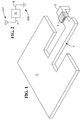
- Figure 1 illustrates a patch 3, constructed of a conductive sheet, or film, such as aluminum.
- the patch need not be the shape shown, and patches are used which are square, rectangular, circular, triangular, linear (that is, a long thin rectangle), and hollow, such as a flat doughtnut shape.
- a feed line 6 is connected to the patch 3.
- Block 9 represents an RFID circuit, which contains the elements described in the Background of the Invention.
- Line 12 represents a ground line, which will be used to connect to a ground plane, later described.
- Lines 6 and 12 are not connected together electrically, as shown by the schematic of Figure 2.
- Line 12 is connected to ground, GND, in the form of a ground plane, later described.
- a signal generator 15, which corresponds to block 9 in Figure 1, generates a signal, which is fed to an antenna ANT, through line 6.
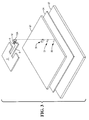
- Figure 3 illustrates structures to which the apparatus of Figure 1 is attached.
- the patch 3 is placed adjacent a sheet 21 of dielectric material, and is bonded to the sheet 21 in a known manner.
- a film 24 of adhesive is placed adjacent the bottom side of the dielectric sheet 21. This adhesive is used to attach the dielectric sheet 21 to a metallic ground plane 27.
- Ground plane 27 can take the form of a metallic sheet, or film, in which case Figure 3 illustrates one embodiment of the invention, in exploded form. In another embodiment, ground plane 27 is provided by a metallic structure to which adhesive film 24 is attached. In this case, Figure 3 illustrates the invention in actual use. However, in this case, the part of the invention which is made or sold would not, in general, include the ground plane 27.
- Leg 12A of line 12 forms a via, or layer-to-layer connection, between the RFID circuit 9 and the ground plane 27.
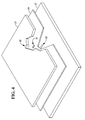
- Window 30, in layer 21, and window 31, in layer 24, allow the leg 12A to pass through the respective layers, en route to the ground plane 27.
- Figure 4 shows the windows in cut-away view.
- Block 33 in Figures 3 and 4 indicates the attachment point of line 12 with the ground plane 27.
- Figure 5 illustrates a sequence of processing steps in one approach to fabricating the apparatus just described.
- the processing begins with what is conceptually a double-sided printed circuit board 45, shown at the upper left part of the Figure.
- the dimensions required of the actual patch antenna may require (1) a different thickness of copper than is obtained with ordinary printed circuit boards, (2) a different thickness of dielectric substrate, and (3) a different dielectric material. If so, it is known in the art how to fabricate board 45 in Figure 5 conforming to those requirements.
- the pattern, indicated by dashed lines 48 on board 45, is etched in the copper on the upper side of the board 45, producing the structure 51, shown at the upper right part of the Figure.
- the copper 52 on the lower side of the board 45 is not etched.
- a via 54 is formed, as indicated at the lower right of the Figure, which connects pad 55 to the ground plane 528.
- the via 54 can be formed by drilling from the bottom of the board to the pad 55, and filling the drilled hole with solder. The entire assembly can then be nickel-plated, to reduce corrosion, and to facilitate later soldering.
- ground plane 52 It may be desirable to make electrical contact between the ground plane 52 and the container 59. This can be accomplished by, for example, abrading a spot (not shown) on the container 60, to remove paint, corrosion, and other unwanted materials. Then the assembly 57 is attached to the container 59, using a conductive adhesive, such as an epoxy containing a powdered metal, such as silver powder.
- a conductive adhesive such as an epoxy containing a powdered metal, such as silver powder.
- Figure 7 illustrates some generally accepted parameters used in the design of patch antennas, and various forms of the invention can be designed using some, or all, of those parameters.
- the symbol that is epsilon-sub-r refers to the relative dielectric constant of the DIELECTRIC in Figure 7.
- Figure 8 illustrates roughly the radiation pattern of a generic patch antenna.
- the Figure is a polar plot of electric field strength. It is emphasized that line 160 does not represent a boundary. That is, line 160 does not indicate that the electric field E is zero at point P1, outside the line 160.
- line 160 indicates the relative electric field strength E, at different angles.
- the relative electric field strength at any point P2 on line L2 is represented by the length of arrow A2.
- the relative electric field strength at any point P3 on line L3, a similar distance from the antenna as point P2, is represented by the length of arrow A3.
- the relative strengths of the two electric fields is represented by the relative sizes of the two arrows.
- FIG. 9 one standard mode of feeding a signal to a patch antenna is shown in Figure 9. Holes H1 and H2, shown in the upper part of the Figure, are cut into the ground plane 248 and the dielectric 221. A coaxial cable connector 250, shown in the lower part of the Figure, is connected as indicated. The shell or sheath S is connected to the ground plane 248. The signal wire W is connected to the patch 203, as indicated by dot D.
- the coaxial cable 250 is located at a position which is removed from the fringing field 250 of Figure 8, and does not interfere with the fringing field 250.
- the RFID circuit 209 occupies the position indicated in Figure 10, on the patch 203. That is, the RFID circuit is located on the top of the patch 203, and the dielectric layer 221 is located on the bottom of the patch 203.
- the RFID circuit 209 can be connected to the patch 203 and the ground plane 248 as indicated in Figures 11 and 12.
- the signal lead 6 of Figures 11 and 1 may largely be eliminated.
- Dot 6A in Figure 12 represents the signal connection to the patch 203, and can take the form of a direct connection between a pad (not shown) on the IC within block 209 and the patch 203. This type of direct connection is discussed again later.
- the RFID circuit 209 in Figure 10 is located entirely within a boundary 350 defined by the periphery of the patch 303. That is, if the dielectric 221 is made the same size as the patch 203, then the entire apparatus is contained within the perimeter 350, which bounds the patch 203 and dielectric 221.
- the RFID circuit 209 can be embedded within the dielectric 221, as shown in Figure 13.
- Signal line 6 and ground line 12 are shown in Figure 14.
- Figure 15 shows a cross-sectional view.
- block 209 may take the form of a die cut from a silicon wafer.
- the RFID circuit is fabricated on that die.
- the RFID circuit will be fabricated on the surface of the die. That is, the transistors, resistors, traces, and so on only penetrate one, or a few, microns into the die.
- a pad may be fabricated on the die, represented by dot D in Figure 14, which can make direct contact with the patch 203. Then line 6 would not be needed, but line 12 would be present, and would connect to the top of the die, where the integrated circuit has been fabricated.
- the dot D could contact the ground plane 248, in which case line 12 would not be needed, but line 6 would be present, running from the surface on the die where the integrated circuit is formed to the patch 203.
- the ground plane 248 in Figure 13 may not be associated with the RFID circuit as manufactured, but may be later provided by a metallic surface onto which the RFID circuit is affixed.
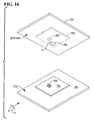
- the lower part of Figure 16 shows a top view of RFID circuit 209 applied to patch 203, which is affixed to dielectric sheet 221.
- Sheet 221 may be manufactured the same size as patch 203.
- the upper part of the Figure shows a view of the bottom of the dielectric sheet 221, as seen by eye E.
- Patch 203 and RFID circuit 209 are drawn in phantom at the top, because the dielectric sheet blocks their view.
- a conductive pad 290 Affixed to the bottom surface of the dielectric sheet 221 is a conductive pad 290, which is connected to the RFID circuit 209, by wire 12, which extends through the dielectric sheet 221.
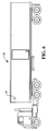
- the overall assembly of Figure 16 is attached to a metallic container, such as that shown in Figure 6.
- the pad 290 of Figure 16 makes contact with the wall of the container. The wall then acts as a ground plane.
- the conductive wall of the container provides the function of the ground plane 27 in Figure 3.
- FIG 17 illustrates another embodiment.
- the RFID circuit 209 is fabricated onto a silicon substrate 300 (or other substrate if silicon technology is not used), which substrate 300 is a die cut from a larger silicon wafer.
- the Inventor points out that the circuit 209 occupies the top surface T of the substrate 300.
- Pads 303 connect with the active part of the IC, AIC, through traces 306.
- the RFID circuit 209 is attached to the patch 203, which is here shown below the dielectric layer 221.
- pads 303 are shown. Many of these can be used for testing purposes, during manufacture of the circuit 209. However, after manufacture, in one form of the invention, only two pads are used in the operative invention, namely, (1) a pad connecting to the signal lead, such as signal lead 6 in Figure 1, and (2) a pad connecting either to the ground plane 27 in Figure 3, or to pad 290 in Figure 17 which, in turn, will later connect to a ground plane, such as the wall of a shipping container.
- the other pads are insulated from the patch 203.
- Pad 303A and 303B connects to pad 290 through via 310.
- Figure 19 is a cross-sectional view. The connection between pad 303A in Figure 18 and the patch 203 is indicated by rectangle 315 in Figure 19.
- one type of RFID tag obtains its operating power from incoming rf radiation, which is received by the tag's antenna.
- that incoming radiation creates the fringing field 250, causing power to flow into the RFID circuit.
- the RFID circuit in the power-absorption mode, can be electrically shielded by the patch 203 from the incoming radiation, yet can derive power from that radiation.
- the RFID circuit 209 in Figure 13 would be shielded from incoming radiation entering from above, by patch 203. Nevertheless, the circuit 209 can absorb energy from the patch antenna.
- circuit 209 in Figure 10 may appear to be exposed to incoming radiation, it is submitted that such is not actually the case.
- the incoming electric field vector can be broken into two components, one parallel with the patch 203, and one perpendicular to the patch 203.
- the RFID circuit 209 in being adjacent to the patch 203, sees a zero field component parallel with the patch 203, at the surface of the patch 203.
- the component which is perpendicular to the patch 203 will be one of the fringing fields 250 in Figure 8. It will extend from, for example, point PA to point PB, roughly indicated by dashed line E. However, the field strength will be equal to (1) the voltage difference between the patch 203 and the ground plane 248, (2) divided by the length of dashed line E. That field strength will be less than that of field line 250.
- the RFID circuit does not directly receive incoming radiation, it nevertheless can derive power from the antenna immersed in the radiation.
- RFID tag an "RFID circuit”
- RFID circuit an electrical circuit, probably an integrated circuit, but lacks an antenna.
- an RFID circuit lacking an antenna, is sufficiently close to a device transmitting data at the frequency for which the RFID circuit is designed, the RFID circuit will pick up that data, using its internal wiring as antenna. Nevertheless, the separate antenna used in normal operation is absent.
- the RFID circuit stores data, and acts as a radio transceiver, which transmits the data. It may perform other functions. It may continually transmit the data, or may do so only when prompted by a polling signal.
- RFID tag is the combination of (1) an RFID circuit with (2) an antenna. That is, the RFID circuit is largely inoperative, without the antenna. (Again, as stated above, the internal conductive traces on the RFID circuit can broadcast RF signals, which can be picked up at short range, without an antenna. However, in ordinary usage, an added antenna is used.)
- RFID tag is a small device, which is ordinarily portable until attached to an object, and which stores a code or number, and transmits that code/number. It may transmit the code/number periodically, or may do so only when prompted by an interrogation signal. It may perform other functions.
- “Small” means (1) at least smaller than a brief case measuring 20 x 18 x 2 inches. “Small” can further mean smaller than 3 x 4 x 0.5 inches. “Small” can further mean smaller than 1 x 1 x 0.2 inches.
- RFID tag One specific type of RFID tag is the passive type, which derives operating power from incoming radiation, and which is not self-powered.
- a specific type of passive RFID tag is the type which performs a single function, namely, transmitting a number stored within it when prompted to do so by an interrogation signal.
- atch antenna is a term-of-art.
- One definition is a section of a strip line, wherein one conductor of the strip line forms a ground plane, and the other conductor, smaller in area than the ground plane, acts as an antenna.
- a specific form of the invention utilizes a patch antenna in connection with a non-self-powered, passive, RFID circuit, operating at frequencies above 900 MHz.
- the ground plane of the patch may take the form of the conductive wall of a shipping container. In such a case, it is expected that the problem of signal nulls discussed above, and other problems caused by nearby conductive objects, will be reduced.
- Patch antennas in general, are characterized by narrow bandwidth, low efficiency, and low gain, compared with antennas commonly used with RFID tags, such as dipole antennas.
- these disadvantages can be offset by the elimination of the problems otherwise caused by the metallic shipping container to which the RFID is attached.
- a self-powered RFID circuit can transmit a stronger signal than a passive RFID circuit, which would imply a higher signal-to-noise ratio, which would imply less significant interference from nearby reflective objects, compared with a passive device.
- the passive RFID circuit would benefit from the patch antenna more than would a self-powered RFID circuit, because the passive RFID is more subject to noise problems.
- RFID tags sometimes contain printed labels.
- a label can overlay part, or all, of the dielectric sheer 21 in Figure 3.
- the label can be printed on the dielectric 21, or can be printed on a separate sheet which is attached to the dielectric 21.
Landscapes
- Engineering & Computer Science (AREA)
- Computer Hardware Design (AREA)
- Microelectronics & Electronic Packaging (AREA)
- Physics & Mathematics (AREA)
- General Physics & Mathematics (AREA)
- Theoretical Computer Science (AREA)
- Computer Networks & Wireless Communication (AREA)
- Waveguide Aerials (AREA)
- Details Of Aerials (AREA)
Applications Claiming Priority (1)
| Application Number | Priority Date | Filing Date | Title |
|---|---|---|---|
| US11/129,094 US7605706B2 (en) | 2005-05-13 | 2005-05-13 | Patch antenna for RFID tag |
Publications (2)
| Publication Number | Publication Date |
|---|---|
| EP1724714A2 true EP1724714A2 (de) | 2006-11-22 |
| EP1724714A3 EP1724714A3 (de) | 2006-12-13 |
Family
ID=36691909
Family Applications (1)
| Application Number | Title | Priority Date | Filing Date |
|---|---|---|---|
| EP06252007A Withdrawn EP1724714A3 (de) | 2005-05-13 | 2006-04-11 | Patchantenne für ein RFID-Etikett |
Country Status (3)
| Country | Link |
|---|---|
| US (1) | US7605706B2 (de) |
| EP (1) | EP1724714A3 (de) |
| JP (1) | JP2006319964A (de) |
Cited By (4)
| Publication number | Priority date | Publication date | Assignee | Title |
|---|---|---|---|---|
| EP1978592A1 (de) * | 2007-04-04 | 2008-10-08 | Valtion Teknillinen Tutkimuskeskus | Fernidentifizierungsvorrichtung und Antennenkonstruktion für ein Fernidentifizierungssystem |
| WO2009011375A1 (ja) | 2007-07-18 | 2009-01-22 | Murata Manufacturing Co., Ltd. | 無線icデバイスおよびその製造方法 |
| EP2330684A4 (de) * | 2008-09-05 | 2011-10-19 | Omron Tateisi Electronics Co | Rfid-etikett, rifid-etikettensatz und rfid-system |
| ITPI20130100A1 (it) * | 2013-12-06 | 2015-06-07 | Studio Angeli Studio Associato In G Angeli F E | Dispositivo per identificare veicoli mediante tecnologia a rfid passivi |
Families Citing this family (23)
| Publication number | Priority date | Publication date | Assignee | Title |
|---|---|---|---|---|
| TWI247449B (en) * | 2005-03-10 | 2006-01-11 | Li Shing Comm Science And Tech | RF antenna with distant identification function |
| KR100659272B1 (ko) * | 2005-12-15 | 2006-12-20 | 삼성전자주식회사 | 과전압 제어가 가능한 무선인증용 태그 및 그의 과전압제어 방법 |
| US20070268142A1 (en) * | 2006-05-17 | 2007-11-22 | Chiu Lihu M | VSWR classification and non-resonant encoding of RFID tags using a near-field encoder |
| US7681301B2 (en) * | 2007-03-07 | 2010-03-23 | James Neil Rodgers | RFID silicon antenna |
| JP4929438B2 (ja) * | 2007-06-07 | 2012-05-09 | 日本信号株式会社 | アンテナ |
| US8344889B2 (en) * | 2007-12-17 | 2013-01-01 | Solstice Medical, Llc | Side loaded shorted patch RFID tag |
| JP5170109B2 (ja) * | 2008-01-07 | 2013-03-27 | 富士通株式会社 | 電子装置、アンテナおよび物品 |
| US7696930B2 (en) * | 2008-04-14 | 2010-04-13 | International Business Machines Corporation | Radio frequency (RF) integrated circuit (IC) packages with integrated aperture-coupled patch antenna(s) in ring and/or offset cavities |
| US8022815B2 (en) * | 2009-10-16 | 2011-09-20 | Kabushiki Kaisha Sato | Magnetic RFID coupler with balanced signal configuration |
| US8730045B2 (en) | 2010-12-16 | 2014-05-20 | Avery Dennison Corporation | Isolating and RFID-based sensor from environmental interference |
| US9147145B2 (en) | 2011-05-31 | 2015-09-29 | United Technologies Corporation | RFID tag system |
| US9590761B2 (en) | 2011-09-23 | 2017-03-07 | Commscope Technologies Llc | Detective passive RF components using radio frequency identification tags |
| US9151741B2 (en) * | 2011-11-02 | 2015-10-06 | Avery Dennison Corporation | RFID-based devices and methods for initializing a sensor |
| CN103839100A (zh) * | 2014-03-13 | 2014-06-04 | 湖南理工学院 | 一种双频两用远距离抗金属rfid无源标签 |
| US11264697B2 (en) * | 2016-10-18 | 2022-03-01 | American Aerogel Corporation | Linked antenna pair for transmission through shielded shipping container |
| JP7108902B2 (ja) * | 2018-03-26 | 2022-07-29 | パナソニックIpマネジメント株式会社 | Icカード及びicカードケース |
| JP6546711B1 (ja) * | 2019-04-10 | 2019-07-17 | 株式会社エスケーエレクトロニクス | 非接触情報担体 |
| JP1675741S (de) * | 2020-05-29 | 2021-01-04 | ||
| JP1734932S (de) * | 2022-09-07 | 2023-01-19 | ||
| USD1094343S1 (en) * | 2024-04-23 | 2025-09-23 | Avery Dennison Retail Information Services Llc | Antenna |
| USD1096704S1 (en) * | 2024-06-25 | 2025-10-07 | Avery Dennison Retail Information Services Llc | Antenna |
| USD1099870S1 (en) * | 2024-07-02 | 2025-10-28 | Avery Dennison Retail Information Services Llc | Antenna |
| USD1101725S1 (en) * | 2024-07-16 | 2025-11-11 | Avery Dennison Retail Information Services Llc | Antenna |
Family Cites Families (15)
| Publication number | Priority date | Publication date | Assignee | Title |
|---|---|---|---|---|
| US632915A (en) * | 1897-11-11 | 1899-09-12 | Edward W Comfort | Paper-trimming guide. |
| US4068232A (en) * | 1976-02-12 | 1978-01-10 | Fairchild Industries, Inc. | Passive encoding microwave transponder |
| AU3465293A (en) | 1992-01-23 | 1993-09-01 | Saab-Scania Combitech Aktiebolag | Device for information transfer |
| DE69324132T2 (de) * | 1992-01-23 | 1999-10-28 | Saab-Scania Combitech Ab, Joenkoeping | Gerät zur drahtlosen informationsübertragung |
| US5995048A (en) * | 1996-05-31 | 1999-11-30 | Lucent Technologies Inc. | Quarter wave patch antenna |
| US5945938A (en) * | 1996-11-14 | 1999-08-31 | National University Of Singapore | RF identification transponder |
| US6215402B1 (en) * | 1998-03-13 | 2001-04-10 | Intermec Ip Corp. | Radio frequency identification transponder employing patch antenna |
| US6329915B1 (en) * | 1997-12-31 | 2001-12-11 | Intermec Ip Corp | RF Tag having high dielectric constant material |
| US6281794B1 (en) * | 1998-01-02 | 2001-08-28 | Intermec Ip Corp. | Radio frequency transponder with improved read distance |
| US6342830B1 (en) * | 1998-09-10 | 2002-01-29 | Xerox Corporation | Controlled shielding of electronic tags |
| AU6403799A (en) | 1998-09-30 | 2000-07-03 | Intermec Ip Corp. | Combination radio frequency identification transponder (rfid tag) and magnetic electronic article suveillance (eas) tag |
| WO2000043952A1 (en) | 1999-01-22 | 2000-07-27 | Intermec Ip Corp. | Rfid transponder |
| JP2000332523A (ja) | 1999-05-24 | 2000-11-30 | Hitachi Ltd | 無線タグ、その製造方法及びその配置方法 |
| US6924688B1 (en) * | 2000-11-28 | 2005-08-02 | Precision Dynamics Corporation | Rectifying charge storage device with antenna |
| FR2832241B1 (fr) * | 2001-11-09 | 2004-04-09 | Allibert Equipement | Dispositif tracable par un identifiant electronique |
-
2005
- 2005-05-13 US US11/129,094 patent/US7605706B2/en not_active Expired - Fee Related
-
2006
- 2006-04-11 EP EP06252007A patent/EP1724714A3/de not_active Withdrawn
- 2006-04-20 JP JP2006116937A patent/JP2006319964A/ja active Pending
Cited By (6)
| Publication number | Priority date | Publication date | Assignee | Title |
|---|---|---|---|---|
| EP1978592A1 (de) * | 2007-04-04 | 2008-10-08 | Valtion Teknillinen Tutkimuskeskus | Fernidentifizierungsvorrichtung und Antennenkonstruktion für ein Fernidentifizierungssystem |
| WO2009011375A1 (ja) | 2007-07-18 | 2009-01-22 | Murata Manufacturing Co., Ltd. | 無線icデバイスおよびその製造方法 |
| EP2169594A4 (de) * | 2007-07-18 | 2010-08-25 | Murata Manufacturing Co | Drahtloses ic-bauelement und herstellungsverfahren dafür |
| US7857230B2 (en) | 2007-07-18 | 2010-12-28 | Murata Manufacturing Co., Ltd. | Wireless IC device and manufacturing method thereof |
| EP2330684A4 (de) * | 2008-09-05 | 2011-10-19 | Omron Tateisi Electronics Co | Rfid-etikett, rifid-etikettensatz und rfid-system |
| ITPI20130100A1 (it) * | 2013-12-06 | 2015-06-07 | Studio Angeli Studio Associato In G Angeli F E | Dispositivo per identificare veicoli mediante tecnologia a rfid passivi |
Also Published As
| Publication number | Publication date |
|---|---|
| JP2006319964A (ja) | 2006-11-24 |
| EP1724714A3 (de) | 2006-12-13 |
| US20060255946A1 (en) | 2006-11-16 |
| US7605706B2 (en) | 2009-10-20 |
Similar Documents
| Publication | Publication Date | Title |
|---|---|---|
| US7605706B2 (en) | Patch antenna for RFID tag | |
| US8672230B2 (en) | RFID tag | |
| Nikitin et al. | Low cost silver ink RFID tag antennas | |
| US7839285B2 (en) | Electronic communication devices, methods of forming electrical communication devices, and communications methods | |
| KR101148268B1 (ko) | Rfid 태그 광대역 로그 나선 안테나 시스템 및 rf신호 수신 방법 | |
| EP2779033B1 (de) | Abgeschirmte hohlraumschlitzentkoppelte RFID-Etiketten | |
| EP3309896B1 (de) | Funkfrequenz-integrierte leiterplattenanordnung mit ball-grid-array für automatisierte fahrzeuge | |
| US6133836A (en) | Wireless communication and identification packages, communication systems, methods of communicating, and methods of forming a communication device | |
| EP1443591A1 (de) | Leiterplattenantenne | |
| JP2004336240A (ja) | Rfidタグ | |
| JP2006042059A (ja) | 無線通信装置及びそのインピ−ダンス調整方法 | |
| KR20100027205A (ko) | Rfid 리더 라이터용 안테나 | |
| EP1898488A1 (de) | Hochfrequenz-identifikationsetikett | |
| KR20160027446A (ko) | Rfid 라벨 프린터용 루프 안테나 및 그 설치방법 | |
| JP4927665B2 (ja) | Rfidタグ用の補助アンテナ及びその取付方法 | |
| US20080315991A1 (en) | Methods and systems of attaching a radio transceiver to an antenna | |
| JP4363409B2 (ja) | Rfidタグ及びその製造方法 | |
| JP2006127424A (ja) | 無線タグ | |
| JPWO2020110930A1 (ja) | Rfidタグ | |
| US8720789B2 (en) | Wireless IC device | |
| US20080297417A1 (en) | Light weight rugged microstrip element antenna incorporating skeleton dielectric spacer | |
| US9665821B1 (en) | Long-range surface-insensitive passive RFID tag | |
| JP5061712B2 (ja) | 非接触icタグの製造方法 | |
| KR101206088B1 (ko) | Rfid 태그 | |
| JP6846042B2 (ja) | Rfタグおよびrfタグ付ナンバープレート |
Legal Events
| Date | Code | Title | Description |
|---|---|---|---|
| PUAI | Public reference made under article 153(3) epc to a published international application that has entered the european phase |
Free format text: ORIGINAL CODE: 0009012 |
|
| PUAL | Search report despatched |
Free format text: ORIGINAL CODE: 0009013 |
|
| AK | Designated contracting states |
Kind code of ref document: A2 Designated state(s): AT BE BG CH CY CZ DE DK EE ES FI FR GB GR HU IE IS IT LI LT LU LV MC NL PL PT RO SE SI SK TR |
|
| AX | Request for extension of the european patent |
Extension state: AL BA HR MK YU |
|
| AK | Designated contracting states |
Kind code of ref document: A3 Designated state(s): AT BE BG CH CY CZ DE DK EE ES FI FR GB GR HU IE IS IT LI LT LU LV MC NL PL PT RO SE SI SK TR |
|
| AX | Request for extension of the european patent |
Extension state: AL BA HR MK YU |
|
| 17P | Request for examination filed |
Effective date: 20070613 |
|
| 17Q | First examination report despatched |
Effective date: 20070716 |
|
| AKX | Designation fees paid |
Designated state(s): DE FR GB IT |
|
| STAA | Information on the status of an ep patent application or granted ep patent |
Free format text: STATUS: THE APPLICATION IS DEEMED TO BE WITHDRAWN |
|
| 18D | Application deemed to be withdrawn |
Effective date: 20101102 |