EP1724818A2 - Verfahren zur Herstellung vollsilicidierter Dual-Gates und mit diesem Verfahren erhältliche Halbleiterbauelemente - Google Patents
Verfahren zur Herstellung vollsilicidierter Dual-Gates und mit diesem Verfahren erhältliche Halbleiterbauelemente Download PDFInfo
- Publication number
- EP1724818A2 EP1724818A2 EP06114050A EP06114050A EP1724818A2 EP 1724818 A2 EP1724818 A2 EP 1724818A2 EP 06114050 A EP06114050 A EP 06114050A EP 06114050 A EP06114050 A EP 06114050A EP 1724818 A2 EP1724818 A2 EP 1724818A2
- Authority
- EP
- European Patent Office
- Prior art keywords
- metal
- layer
- silicidation
- gate
- nisi
- Prior art date
- Legal status (The legal status is an assumption and is not a legal conclusion. Google has not performed a legal analysis and makes no representation as to the accuracy of the status listed.)
- Withdrawn
Links
Images






Classifications
-
- H—ELECTRICITY
- H10—SEMICONDUCTOR DEVICES; ELECTRIC SOLID-STATE DEVICES NOT OTHERWISE PROVIDED FOR
- H10D—INORGANIC ELECTRIC SEMICONDUCTOR DEVICES
- H10D64/00—Electrodes of devices having potential barriers
- H10D64/01—Manufacture or treatment
- H10D64/013—Manufacture or treatment of electrodes having a conductor capacitively coupled to a semiconductor by an insulator
- H10D64/01302—Manufacture or treatment of electrodes having a conductor capacitively coupled to a semiconductor by an insulator the insulator being formed after the semiconductor body, the semiconductor being silicon
- H10D64/01304—Manufacture or treatment of electrodes having a conductor capacitively coupled to a semiconductor by an insulator the insulator being formed after the semiconductor body, the semiconductor being silicon characterised by the conductor
- H10D64/01318—Manufacture or treatment of electrodes having a conductor capacitively coupled to a semiconductor by an insulator the insulator being formed after the semiconductor body, the semiconductor being silicon characterised by the conductor the conductor comprising a layer of alloy material, compound material or organic material contacting the insulator, e.g. TiN
- H10D64/0132—Manufacture or treatment of electrodes having a conductor capacitively coupled to a semiconductor by an insulator the insulator being formed after the semiconductor body, the semiconductor being silicon characterised by the conductor the conductor comprising a layer of alloy material, compound material or organic material contacting the insulator, e.g. TiN the conductor being a metallic silicide
-
- H—ELECTRICITY
- H10—SEMICONDUCTOR DEVICES; ELECTRIC SOLID-STATE DEVICES NOT OTHERWISE PROVIDED FOR
- H10D—INORGANIC ELECTRIC SEMICONDUCTOR DEVICES
- H10D64/00—Electrodes of devices having potential barriers
- H10D64/60—Electrodes characterised by their materials
- H10D64/66—Electrodes having a conductor capacitively coupled to a semiconductor by an insulator, e.g. MIS electrodes
- H10D64/667—Electrodes having a conductor capacitively coupled to a semiconductor by an insulator, e.g. MIS electrodes the conductor comprising a layer of alloy material, compound material or organic material contacting the insulator, e.g. TiN workfunction layers
- H10D64/668—Electrodes having a conductor capacitively coupled to a semiconductor by an insulator, e.g. MIS electrodes the conductor comprising a layer of alloy material, compound material or organic material contacting the insulator, e.g. TiN workfunction layers the layer being a silicide, e.g. TiSi2
-
- H—ELECTRICITY
- H10—SEMICONDUCTOR DEVICES; ELECTRIC SOLID-STATE DEVICES NOT OTHERWISE PROVIDED FOR
- H10D—INORGANIC ELECTRIC SEMICONDUCTOR DEVICES
- H10D84/00—Integrated devices formed in or on semiconductor substrates that comprise only semiconducting layers, e.g. on Si wafers or on GaAs-on-Si wafers
- H10D84/01—Manufacture or treatment
- H10D84/0123—Integrating together multiple components covered by H10D12/00 or H10D30/00, e.g. integrating multiple IGBTs
- H10D84/0126—Integrating together multiple components covered by H10D12/00 or H10D30/00, e.g. integrating multiple IGBTs the components including insulated gates, e.g. IGFETs
- H10D84/0165—Integrating together multiple components covered by H10D12/00 or H10D30/00, e.g. integrating multiple IGBTs the components including insulated gates, e.g. IGFETs the components including complementary IGFETs, e.g. CMOS devices
- H10D84/0172—Manufacturing their gate conductors
- H10D84/0174—Manufacturing their gate conductors the gate conductors being silicided
-
- H—ELECTRICITY
- H10—SEMICONDUCTOR DEVICES; ELECTRIC SOLID-STATE DEVICES NOT OTHERWISE PROVIDED FOR
- H10D—INORGANIC ELECTRIC SEMICONDUCTOR DEVICES
- H10D84/00—Integrated devices formed in or on semiconductor substrates that comprise only semiconducting layers, e.g. on Si wafers or on GaAs-on-Si wafers
- H10D84/01—Manufacture or treatment
- H10D84/02—Manufacture or treatment characterised by using material-based technologies
- H10D84/03—Manufacture or treatment characterised by using material-based technologies using Group IV technology, e.g. silicon technology or silicon-carbide [SiC] technology
- H10D84/038—Manufacture or treatment characterised by using material-based technologies using Group IV technology, e.g. silicon technology or silicon-carbide [SiC] technology using silicon technology, e.g. SiGe
Definitions
- the present invention relates to semiconductor process technology and devices.
- the present invention relates to semiconductor devices with metallic gate electrodes formed by a reaction between a metal and a semiconductor material.
- Metal gates are expected to replace partially silicided poly-Si gates in future complementary metal-oxide-semiconductor (CMOS) technology nodes, in order to eliminate poly-Si depletion issues.
- CMOS complementary metal-oxide-semiconductor
- WF work function
- silicides as metal gate electrodes, and in particular, on NiSi fully-silicided (FUSI) gates.
- Ni-silicide appears as an attractive metal gate candidate that allows maintaining several aspects of the flows from previous generations (such as Si gate pattern and etch, and self-aligned silicide processes).
- a key property that has attracted attention to NiSi FUSI gates is the modulation of their effective work function on SiO 2 by dopants which may allow for tuning of the threshold voltage (V t ) of nMOS and pMOS devices without the need for two different metals.
- V t threshold voltage
- the present invention relates to a method of manufacturing a fully-silicided-gate electrode in a semiconductor device, comprising the steps of:
- said semiconductor layer comprises (or consists of) silicon and/or germanium, more preferably comprises (or consists of) poly-silicon (poly-Si).
- said metal layer comprises (or consists of) any suitable refractory metal, noble metal, transition metal, or any combination thereof. More preferably, said metal layer comprises (or consists of) Ni.
- said first thermal budget can be determined by a silicidation kinetics graph (such as the silicidation kinetics graph represented by figure 6) drawn up for each silicide phase, M x S y , envisaged in the partially silicided gate, wherein M represents said metal and S said semiconductor used, and wherein x and y are real numbers different from 0 and higher than 0.
- a silicidation kinetics graph such as the silicidation kinetics graph represented by figure 6
- the step of providing said first thermal budget consists of an Rapid Thermal Processing (RTP).
- RTP Rapid Thermal Processing
- the step of providing said second thermal budget consists of an RTP.
- the step of removing said remaining metal layer consists of a selective etching.
- said metal layer consists of Ni and said semiconductor layer consists of poly-Si.
- said first thermal budget is such that a Ni 2 Si layer is grown, with a thickness comprised between 0,9 and 1,5 of the poly-Si thickness, whereby a NiSi FUSI gate is obtained.
- a method according to the invention for manufacturing a fully-silicided-gate electrode in a MOSFET device comprises the steps of:
- Said first thermal budget can be determined by a silicidation kinetics graph drawn up for each silicide phase, Ni x Si y , envisaged in the partially silicided gate, wherein x and y are real numbers different from 0 and higher than 0 and wherein 1 ⁇ x/y ⁇ 3.
- said first thermal budget is such that a Ni 2 Si layer is grown, with a thickness comprised between 0,9 and 1,5 of the poly-Si thickness, whereby a NiSi FUSI gate is obtained.
- said poly-Si layer is upon a SiON or upon a HfSiON layer.
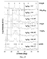
- Figure 1 represents XRD spectra showing formation of NiSi, Ni 2 Si and Ni 3 Si by adjusting Ni to Si thickness ratio.
- Figure 2 represents the increase in resistivity and silicide thickness with increasing Ni to Si thickness ratio.
- Figure 3 represents CV curves for FUSI devices, showing larger V FB shifts from NiSi to Ni 3 Si on HfSiON (330 mV) than on SiON (100 mV).
- Figure 4 represents the WF for the main Ni silicide phases.
- the large difference for NiSi between SiO 2 and HfSiON disappears for larger Ni contents indicating unpinning of the FL.
- Figure 5 represents schematic processes showing 1-step and 2-step FUSI processes on wide and narrow gates, for varying Ni and Si thicknesses. Due to Ni diffusion from top of spacers, the effective Ni/Si ratio can be larger for narrow devices than for large structures.
- Figure 6 represents Ni 2 Si silicidation kinetics showing diffusion limited growth.
- Figure 7 represents silicide growth rates for NiSi and Ni 2 Si.
- Figure 8 represents R s vs. L showing linewidth effect for 60 nm Ni 1-step FUSI eliminated with 2-step FUSI.
- Figure 9 represents TEM cross sections of narrow FUSI gates for 1-step and 2-step FUSI processes.
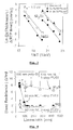
- Figure 10 represents V t roll-off for 1-step and 2-step Ni FUSI/HfO 2 processes.
- the kink seen for the 1-step process is due to transition from NiSi for long gate lengths to Ni rich silicide on short ones.
- Figure 11 represents V t roll-off for Ni FUSI/SiON processes.
- t NI /t Si 0.6 (targeting NiSi)
- the 1-step process shows a kink corresponding to the transition from NiSi at long gate lengths to Ni rich silicide at short gate lengths.
- Ni 3 Si and 2-step NiSi FUSI processes show smooth V t roll-off to 30 nm gate lengths.
- Figure 12 represents V t roll-off for Ni FUSI/HfSiON showing scalability with smooth roll-off for Ni 3 Si and 2-step NiSi FUSI processes.
- Figure 13 represents R s vs. RTP1 temperature for 2-step Ni FUSI process.
- the increase in R s with increasing temperature for 50 nm gates is due to the transition from NiSi to Ni-rich silicide.
- Figure 14 represents a RTP1 process window for 2-step NiSi FUSI process. Process margins need to be added to account for process variations and silicide reaction non-uniformity (b) and (c).
- Figure 15 represents XRD patterns of Ni-silicide on SiO 2 films for deposited Ni to poly-Si thickness ratios (t Ni /t Si ) between 0.3 and 0.9.
- Figure 16 represents RBS spectra of Ni-silicide on SiO 2 films for deposited Ni to poly-Si thickness ratios (t NI /t Si ) between 0.6 and 0.9.
- Figure 17 represents a cross-section TEM of Ni FUSI gate stack showing bi-layer structure. NiSi was identified in the lower layer by Fourier-transformed high-resolution images. EDX showed a higher Ni/Si composition ratio for the top layer.
- Figure 18 represents RBS spectra of Ni-silicide on SiO 2 films for deposited Ni to poly-Si thickness ratios (t Ni /t Si ) of 0.6 and 1.1 (1 MeV 4 He ++ , 160°).
- Figure 19 represents XRD patterns of Ni-silicide on SiO 2 films for deposited Ni to poly-Si thickness ratios (t Ni /t Si ) between 0.6 and 1.7. Results for different silicidation processes are shown for selected thickness ratios (LT and HT indicate lower and higher temperature processes respectively).
- Figure 20 represents RBS spectra of Ni-silicide on SiO 2 films for deposited Ni to poly-Si thickness ratios (t Ni/ t Si ) of 0.6 to 1. 7 (2 MeV 4 He ++ , 160°).
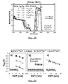
- Figure 21 represents flat band voltage vs. EOT for (a) NiSi/SiO 2 , (b) NiSi/HfSiON/SiO 2 and (c) Ni 2 Si/SiO 2 capacitors showing the effect of dopants.
- Figure 22 represents CV curves comparing NiSi and Ni 3 Si FUSI gates for (a) SiON and (b) HfSiON dielectrics.
- Figure 23 schematically illustrates a method according to the present invention.
- Figure 24 shows XRD (Cu K ⁇ radiation) characterization of Ni silicide films as function of RPT1 temperature according to an example.
- Figure 25 shows the reacted nickel to silicon ratio of Ni silicide films as function of the RPT1 temperature according to an example.
- the metal / semiconductor ratio is not well defined: the metal from top of spacers and surrounding areas can diffuse and react with the semiconductor in the gate, to increase the effective metal / semiconductor ratio.
- a new method for manufacturing a fully-silicided-gate device is described that can eliminate the linewidth dependence existing in previous silicidation methods.
- a method according to the invention for manufacturing a fully-silicided-gate in a semiconductor device comprises the steps of:
- said metal layer can be of any metal(s) preferably capable of diffusing into the underlying semiconductor material and suitable for metal gate electrodes. More particularly, said metal layer can comprise or consists of a refractory metal such as tantalum or tungsten, a noble metal such as Pt, a near noble metal such as Ni, a transition metal such as Ti, or any combination of two or more of these metals.
- a refractory metal such as tantalum or tungsten
- a noble metal such as Pt
- a near noble metal such as Ni
- a transition metal such as Ti
- Said semiconductor layer can be of any material(s) suitable for metal gate electrodes. More particularly, said semiconductor layer can comprise or consists of Si, Ge or a mixture thereof.
- the first thermal step consists of providing a temperature (also referred to as thermal energy), T°1, within a determined period of time.
- T°1 is preferably smaller than the temperature applied in the second thermal step, T°2.
- said first thermal step consists of a Rapid Thermal Processing (RTP1)step.
- RTP1 Rapid Thermal Processing
- said temperature is applied within a period of time varying between about 30 seconds and about 60 seconds.
- the second thermal step consists of providing a temperature, T°2, preferably higher than T°1, within a determined period of time, preferably within a period of time varying between about 30 seconds and about 60 seconds.
- said second thermal step consists of a Rapid Thermal Processing (RTP2) step.
- RTP2 Rapid Thermal Processing
- Limiting T°1 and the period of time aims at controlling the reaction between said metal and said semiconductor such that a metal-rich silicide layer is grown while a certain thickness of said semiconductor layer remains unreacted.
- the terms "silicide”, “silicided”, “silicidation” can refer to the reaction between a metal and silicon, but is not intended to be limited to silicon. For instance, the reaction of a metal with Ge, or any other suitable semiconductor material, may still be referred to as silicidation.
- metal-rich silicide refers to the material resulting from the reaction between said metal and said semiconductor, wherein the ratio metal-to-semiconductor is larger than 1.
- the silicide phase (also referred to as metal-semiconductor phase) can be represented by the formula M x S y , wherein M represents the metal, S represents the semiconductor and wherein x and y are integers or real numbers different from 0. In a metal-rich silicide (phase), x/y is larger than 1.
- the work function thereof may depend on the specific phase in which the alloy is formed.
- the suitability of such metal-semiconductor combinations as gate electrode for one type of transistor depends on which phase of this combination can be formed for this type of transistor.
- Said specific phase is to be formed at least at the bottom part of the gate electrode, the last few nanometers of the gate electrode (e.g. the last nanometer, or the last 2, 3, 4, 5, 10 nanometers or even more), i.e. at least at the part which is the nearest to the gate dielectric, also referred to in the present invention as the "interface".
- the term "interface”, when referring to the silicide phase of the gate electrode, refers to the bottom part of the gate electrode (which is the nearest to the gate dielectric), of few nanometers thickness, e.g. between about 1 nm and about 10 nm, preferably between about 1 nm and about 5 nm.
- Ni 2 Si, Ni 31 Si 12 , Ni 3 Si are Ni-rich silicides.
- the ratio x/y is higher than 1 and preferably less than or equal to 3 (i.e. 1 ⁇ x/y ⁇ 3), while for metal-poor phases, such as NiSi or NiSi 2 , the ratio x/y is higher than 0 and less than or equal to 1 (i.e. 0 ⁇ x/y ⁇ 1).
- said metal-rich silicide layer obtained after said first thermal step has a ratio metal-to-semiconductor (x/y) larger than 1.
- said metal-rich silicide layer can act as the only source of metal during said second thermal step to fully silicide the semiconductor layer.
- the total amount of metal in the fully silicided gate is the amount of metal that is stored in said metal-rich silicide layer after the step of removing the remaining metal.
- the only metal available for the reaction in the second thermal step is the amount of metal incorporated in said metal-rich silicide layer. In the second thermal step only a redistribution of this fixed amount of metal occurs.
- the total amount of metal present in said fully silicided gate to be manufactured can thus be determined.
- Said determined total amount of metal is also the amount of metal that is to be incorporated in the partially silicided semiconductor layer (obtained after said first thermal step), which is the only source of metal after the removal of the remaining, unreacted metal layer.
- the metal diffusion rate, in the reaction metal / semiconductor is controlled in a method of the invention, by providing a thermal budget (T°1 and time) based on a silicidation kinetics graph pre-established for each silicide phase.
- T°1 and time parameters can be determined for each silicide phase by establishing a silicidation kinetics graph, such as the Ni 2 Si silicidation kinetics graph drawn up and represented in figure 6.
- a method of the invention can thus further comprise the step of establishing a silicidation kinetics graph for determining T°1 and the time to be applied in said first thermal step.
- the metal layer consists of Ni and the semiconductor material consists of poly-Si.
- the effective Ni/Si ratio is controlled by limiting the first thermal budget, growing a Ni-rich silicided layer, wherein the poly-Si layer is not fully consumed.
- the unreacted Ni on top of the Ni-rich silicided layer (if any), on the spacers and surrounding areas are then removed, preferably in a selective etching step.
- a second thermal budget is applied to fully silicide the gate.
- the first thermal step consists of providing a temperature T°1 during a period of time, both determined on the basis of a silicidation kinetics graph established for each silicide phase.
- the second thermal step consists of providing a temperature T°2 during a period of time, also determined on the basis of a silicidation kinetics graph.
- the Ni-rich phase in the partially silicided layer can be any Ni x Si y phase(s), wherein x/y is larger than 1, preferably equal or larger than 2.
- the metal-rich silicide in the partially silicided layer can be a Ni x Si y silicide with x/y ⁇ 2 (more particularly with 2 ⁇ x/y ⁇ 3).
- the Ni-rich phase in the partially silicided layer can be Ni 2 Si and/or Ni 3 Si 2 .
- T°1 and the time period of the first thermal step are determined on the basis of figure 6.
- T°1 can be comprised between about 240°C and about 700°C, is preferably smaller than 500°C, more preferably comprised between about 240°C and 350°C.
- T°1 is applied during a period of time varying between about 30 seconds and about 60 seconds.
- said first thermal step consists of a Rapid Thermal Processing (RTP1).
- RTP1 Rapid Thermal Processing
- T°2 can be comprised between about 350°C and about 900°C, is preferably higher than 500°C, more preferably comprised between 500°C and about 850°C.
- T°2 is applied during a period of time varying between about 30 seconds and about 60 seconds.
- said second thermal step consists of a Rapid Thermal Processing (RTP2).
- RTP2 Rapid Thermal Processing
- the effective (reacted) Ni/Si ratio is controlled by limiting the RTP1 thermal budget, growing a Ni-rich silicided that does not fully consume the poly-Si thickness. Excess Ni and Ni films on top of spacers / surrounding areas are then removed in the selective etch step. A second RTP step at a higher temperature is then used to grow NiSi, fully siliciding the gates.
- the present invention can also be described as follows.
- V t and WF shifts are larger on high-K (HfO 2 (250 mV) or HfSiON (330mV)) than on SiON (110mV) and report Fermi level unpinning for Ni-rich FUSI on high-K.
- Ni FUSI gates have recently attracted attention as metal gate candidates for scaled CMOS technologies (Cf. B. Tavel et al., IEDM Tech. Dig., 825 (2001 ); J. Kedzierski et al.,IEDM Tech. Dig., 247 (2002), 441 (2003); K. G. Anil et al., Symp. VLSI Tech., 190 (2004 ); A. Veloso et al., IEDM Tech. Dig., 855 (2004 ); K. Takahashi et al., IEDM Tech. Dig., 91 (2004 )).
- NiSi, NiSi 2 and Ni 3 Si have been studied as possible gate materials. Due to its high nucleation temperature, NiSi 2 is less attractive for integration into self-aligned FUSI gate processes. The scalability of Ni FUSI gate processes to small gate lengths critical for advanced CMOS applications has not yet been addressed in detail, and is the focus of this work.
- MOSFET devices with Ni FUSI gates were fabricated using a self-aligned process with independent silicidation of the source/drain (S/D) and the poly-Si gate using a CMP approach as described in K. G. Anil et al., Symp. VLSI Tech., 190 (2004 ) and in A. Veloso et al., IEDM Tech. Dig., 855 (2004 ).
- S/D source/drain
- CMP approach as described in K. G. Anil et al., Symp. VLSI Tech., 190 (2004 ) and in A. Veloso et al., IEDM Tech. Dig., 855 (2004 ).
- Different Ni/Si ratios were used to obtain the different Ni silicide phases and study their formation as function of gate length. Physical characterization included TEM, SEM, RBS and XRD (RBS and XRD only for blanket films).
- the silicide phase can be effectively controlled by the Ni/Si thickness ratio (t Ni /t Si ), when sufficient thermal budgets are used to drive the reaction to completion (Figs. 1, 2).
- NiSi 2 grows by a nucleation-controlled process and does not form uniformly below 600C, so that incomplete silicidation is seen for t Ni /t Si ⁇ 0.5.
- stacks with NiSi at the bottom and Ni-rich silicide layers on top are formed.
- t Ni /t Si >1.7 Ni 3 Si is the stable phase, and the excess Ni is removed in the selective etch step.
- the resistivity and thickness of the silicide films increase with increasing Ni/Si ratio (Fig. 2).
- CV measurements performed on FUSI devices showed larger V FB shifts with change in Ni/Si composition ratio for HfSiON than for SiON (330 and 100 mV respectively, between NiSi and Ni 3 Si, Fig.
- Ni/Si ratio is not well defined: Ni from top of spacers and surrounding areas can diffuse and react with poly-Si in the gate to increase the effective Ni/Si ratio (Fig. 5).
- Ni silicide phase sequence Ni 2 Si grows at low temperatures by Ni diffusion-limited kinetics (Fig. 6), while NiSi growth follows at higher temperatures with same type of kinetics (Fig. 7), only if available Ni is fully consumed and poly-Si is not. If the Ni supply is not limited, the reaction reaches completion with full Ni 3 Si silicidation. As a consequence, a FUSI linewidth-effect is found for conventional 1-step FUSI processes.
- the kink is of ⁇ 250 mV on HfO 2 and of ⁇ 110 mV on SiON, consistent with the difference in WF between NiSi and Ni 3 Si.
- the gate lengths at which the transition occurs depends on the thermal budget used (of magnitude of the Ni-rich silicide thickness grown at that thermal budget) and can also depend on details of the geometry (spacer height, etc.).
- a split of V t showing a bi-modal distribution that correlates well with RS values (low V t -high RS on PMOS) was observed at the transition gate length.
- NiSi FUSI a 2-step NiSi FUSI process
- the effective (reacted) Ni/Si ratio is controlled by limiting the RTP1 thermal budget, growing a Ni-rich silicide that does not fully consume the poly-Si thickness. Excess Ni and Ni films on top of spacers/surrounding areas are then removed in the selective etch step. A second RTP step at a higher temperature is then used to grow NiSi, fully siliciding the gates.
- FIG. 13 shows the effect of RTP1 temperature on sheet resistance of 50 nm and 1000 nm gates for 60nm Ni/100 nm poly-Si, showing the convergence of RS values with decreasing RTP1 temperature, corresponding to the transition from Ni-rich to NiSi on 50 nm gates.
- the RTP1 thermal budget needs to be controlled such that the grown Ni 2 Si layer has a thickness between 0.9 and 1.5 of the poly-Si thickness, to avoid incomplete silicidation and full silicidation with Ni-rich silicide respectively.
- the RTP1 process window estimated from Ni 2 Si kinetic data (Figs. 6 and 7) is shown in Fig. 14. Margins for process variations and the intrinsic non-uniformity of silicidation need to be taken into account, making the process window ⁇ 20 C.
- Figs. 8 and 9 show that a 2-step NiSi FUSI process can eliminate the linewidth dependence, allowing the growth of NiSi on large and small structures. Smooth V t roll-off for the 2-step NiSi FUSI process further confirms that NiSi can be maintained to small gate lengths (Figs. 11, 12).
- Ni-silicide phases and morphology in Ni fully silicided gates were investigated for varying deposited Ni to Si thickness ratios and rapid thermal processing conditions.
- the presence of NiSi 2 , NiSi, Ni 3 Si 2 , Ni 2 Si, Ni 31 Si 12 and Ni 3 Si as predominant phases was observed for increasing Ni to Si thickness ratios. In most samples typically two of these phases were detected by X-ray diffraction. No secondary phases were detected on Ni 3 Si samples (Ni/Si thickness ratio ⁇ 1.7).
- RBS and TEM analysis confirmed a layered structure with NiSi at the interface and a Ni-rich silicide layer (Ni 2 Si, Ni 3 Si 2 ) on top.
- Metal gates are expected to replace partially silicided poly-Si gates in future complementary metal-oxide-semiconductor (CMOS) technology nodes, in order to eliminate poly-Si depletion issues.
- CMOS complementary metal-oxide-semiconductor
- WF work function
- Ni-silicide appears as an attractive metal gate candidate that allows maintaining several aspects of the flows from previous generations (such as Si gate pattern and etch, and self-aligned silicide processes).
- a key property that has attracted attention to NiSi FUSI gates is the modulation of their effective work function on SiO 2 by dopants, which may allow for tuning of the threshold voltage (V t ) of NMOS and PMOS devices without the need for two different metals.
- V t threshold voltage
- Ni/poly-Si/dielectric stacks were deposited on (100) Si wafers, for varying film thicknesses, in the 30-170 nm and 60-100 nm ranges for Ni and Si films respectively.
- Dielectric films used in this study included SiO 2 , SiON, HfSiON and HfSiON/SiO 2 stacks of varying thicknesses with equivalent oxide thickness (EOT) in the 1-20 nm range.
- Samples were reacted by rapid thermal processing (RTP) to form silicide films at temperatures in the 280-850 °C range, typically for 30 to 60 s.
- RTP rapid thermal processing
- a wet etch used in self-aligned Ni-silicide processes was subsequently performed.
- a second RTP anneal step was performed after the selective etch.
- Samples were characterized by X-ray diffraction (XRD) using Cu-K ⁇ radiation, transmission electron microscopy (TEM), scanning electron microscopy (SEM) and Rutherford backscattering spectrometry (RBS).
- XRD X-ray diffraction
- TEM transmission electron microscopy
- SEM scanning electron microscopy
- RBS Rutherford backscattering spectrometry
- Patterned fully silicided gate devices were also fabricated for electrical characterization, using a chemical-mechanical polishing (CMP) flow as described in reference [4] or a conventional flow (the latter used only for fabrication of capacitors overlapping isolation). Ion implantation was performed on selected samples after poly-Si deposition, with some of these samples receiving an activation anneal.
- CMP chemical-mechanical polishing
- Ni-rich phases form first at low temperatures (Cf. A. Nicolet, S. S. Lau, in N. G. Einspruch and G. B. Larrabee (eds.), VLSI Electronics: Microstructure Science, Vol. 6, Ch. 6, Academic Press, New York (1983 ); and C. Lavoie, F. M. d'Heurle, C. Detavernier and C. Cabral Jr., Microelectronic Engineering, 70, (2003) 144 ).
- Ni 31 Si 12 has been reported at early stages of the reaction, followed by formation of Ni 2 Si.
- Ni 2 Si is generally the predominant phase at low temperatures and early stages of the reaction, forming a layer that grows by diffusion-limited kinetics.
- NiSi nucleates and grows also by diffusion-limited kinetics.
- the presence of Ni 3 Si 2 has also been reported during early stages of the reaction, before nucleation of NiSi.
- the formation of the different Ni-rich silicide phases can also depend on film thickness and thermal history (ramp rates, etc.) during the reaction. As the reaction proceeds for the case of a Nifilm on a Si substrate, NiSi grows fully consuming the Ni-rich silicides. NiSi 2 nucleates and grows at higher temperatures.
- deposited Ni films are reacted with either amorphous or polycrystalline Si films of limited thickness, deposited on top of a dielectric.
- the deposited Ni thickness to Si thickness ratio controls (in combination with the thermal history) the reacted Ni/Si ratio and phases obtained. It is essential for gate electrode applications that the silicide phase at the dielectric interface be well controlled, in order to ensure good control of the V t of devices.
- the phases and morphology after full silicidation for varying t Ni /t Si ratios and thermal processes were investigated, in order to assess and identify conditions for formation of gates with a controlled silicide phase at the dielectric interface.
- NiSi 2 films with NiSi as secondary phase were obtained for t Ni /t Si ⁇ 0.30-035 at 800 °C (Fig. 15).
- the nucleation-controlled growth mechanism of NiSi 2 and its high nucleation temperature make it a less appealing candidate. If processing temperatures are kept below the nucleation temperature of NiSi 2 , a minimum t Ni /t Si ratio of ⁇ 0.55 is required to allow full silicidation of the gate with NiSi. A larger t Ni /t Si ratio (e.g.
- 0.6 is desirable, however, to ensure full silicidation and prevent the presence of Si grains at the dielectric interface, allowing for possible process variations in deposited film thickness.
- bi-layer silicide films are typically obtained with NiSi at the bottom and a Ni-rich silicide on top (Figs. 15 to 17).
- the thickness of each layer depends on the Ni/Si ratio, with a larger proportion of Ni-rich silicide as the ratio is increased (Figs. 15 and 16).
- the phases present in the upper Ni-rich silicide layer can depend on the Ni/Si ratio chosen and on the thermal history.
- XRD patterns and RBS spectra after silicidation (and selective etch) for samples with deposited t Ni /t Si in the 0.6 to 1.7 range (100 nm poly-Si) are shown in Figs. 19 and 20 respectively.
- samples targeting NiSi a slightly Ni-richer ratio rather than the exact stoichiometric ratio was used for samples targeting the different silicide phases.
- Fig. 19 shows that Ni-silicide phases with increasing Ni content are observed by XRD as the Ni/Si ratio is increased.
- t Ni /t Si is increased above ⁇ 0.9, poly-Si is consumed with formation of Ni-rich silicide phases and NiSi does not form.
- Ni FUSI gates were extracted from capacitance-voltage (CV) measurements performed on devices for several dielectric EOT values.
- a dual thickness series with HfSiON/SiO 2 stacks of varying SiO 2 and HfSiON thicknesses was used to evaluate the WF of NiSi on HfSiON, accounting for the effect of bulk charges in HfSiON.
- Figure 21 shows the dependence of the flat band voltage (V fb ) on EOT for NiSi/SiO 2 , NiSi/HfSiON/SiO 2 and Ni 2 Si/SiO 2 gate stacks, and the effect of dopants.
- FIG. 21 (c) shows that the WF of undoped Ni 2 Si on SiO 2 ( ⁇ 4.7 eV) is quite similar to that of NiSi on SiO 2 .
- the WF of Ni 2 Si on SiO 2 appears not to be affected significantly by the addition of dopants.
- Fig. 22 (a) shows that for Ni 3 Si/SiON, an increase in V fb of ⁇ 100 mV from the value for NiSi/SiON is obtained.
- the change in V fb with silicide phase is quite larger for the case of HfSiON, with an increase of >300 mV from NiSi to Ni 3 Si (Fig. 22 (b)), and suggests unpinning of the Fermi level with Ni 3 Si.
- Ni FUSI gates were studied for varying Ni to Si thickness ratios.
- the presence of NiSi 2 , NiSi, Ni 3 Si 2 , Ni 2 Si, Ni 31 Si 12 and Ni 3 Si as predominant phases was obtained for increasing Ni to Si ratios.
- a slightly Ni-richer thickness ratio than that corresponding to stoichiometric NiSi was found suitable for NiSi FUSI gate applications, resulting in a layered structure with NiSi at the interface and a Ni-rich silicide layer on top. No secondary phases were detected on Ni 3 Si samples (Ni to Si thickness ratio ⁇ 1.7). Electrical characterization for NiSi, Ni 2 Si and Ni 3 Si devices on SiO 2 , SiON and high-K dielectrics was performed.
- a method according to the present invention comprises selecting parameters of first thermal step to control diffusion of metal into semiconductor such that the (total) amount of metal present in the silicided portion of the semiconductor gate electrode is well-controlled and the ratio metal-to-semiconductor is larger than 1.
- the metal is the moving species silicidation process and the pile-up of metal in the semiconductor is controlled.
- Preferably abundant metal is present during the first thermal step and hence no metal shortage is likely to occur which would impact the amount of metal incorporated in the semiconductor gate electrode during the first thermal step.
- the semiconductor gate electrode has limited dimensions, i.e. it is not a complete substrate. Consequently all semiconductor material of the gate electrode will be consumed during complete silicidiation.
- the semiconductor gate constitutes a container for accepting the metal and the whole container can take part in the overall silicidation process.
- the process parameters of the silicidation process can be determined as described herein and/or as illustrated in figure 23.
- Figure 23(i) shows the stack of unreacted metal M and semiconductor gate electrode S. For simplicity the sidewall spacers adjacent to the gate electrode and the source/drain regions present in the substrate on which the gate is formed are not shown.
- Figure 23(ii) shows the partially silicided gate electrode after the first thermal step and after having selectively removed the unreacted metal M.
- Figure 23(iii) shows the fully silicided gate electrode after the second thermal step.
- a method according to the invention can further comprise:
- the correlation between the thickness of the fully silicided gate electrode (t 3 ), and the thickness of the unsilicided semiconductor gate (t 1 ), can be made if the metal phase M x3 S y3 is determined.
- the total amount of metal in the fully silicided gate is the amount of metal that has to be stored in the partially silicided semiconductor gate during the first thermal step. Hence after the first thermal step a metal-rich silicide phase is to be formed.
- the only metal available for the use in the second thermal step is the amount of metal incorporated in the semiconductor gate during the first thermal step. In the second thermal step only a redistribution of this incorporated amount of metal will occur.
- the parameters of the first thermal step can be determined by establishing a graph indicating how much metal diffuses into the semiconductor gate electrode for a given time and temperature.
- the suitable time and temperature settings are thus selected such as to have the necessary amount of metal incorporated in a part of the semiconductor gate.
- this amount of metal can be regarded as proportional to t 3 *x 3 and to t 2 *x 2 .
- the total number of metal atoms available before and after the first thermal step can be compared.
- Figures such as figure 6 can be used for each silicide phase M x2 S y2 , since such figures are representative of the amount of metal (x 2 *t 2 ) that can be stored for a given time temperature combination with only thickness t 2 as parameter.
- Such curves can be made by any person skilled in the art using known experimental techniques: select a metal, deposit the selected metal with on a semiconductor substrate, vary time and temperature of the first thermal step and measure the phase x 2 , y 2 and the thickness t 2 of the thus formed silicide phase.
- Figure 14 shows the result of the second thermal step.
- Figure 24 shows the crystallographic characterization of silicide films manufactured using a manufacturing process as illustrated by figure 5.
- the silicide films are characterized using X-ray Diffraction (XRD).
- the gate dielectric is a hafnium-siliconoxide-nitride dielectric.
- the two-step thermal process is performed using an ASM Levitor RTP system.
- the temperature of the first thermal step (RTP1) is varied from about 340°C to about 675°C.
- the time of this first thermal step was set at about 30s.
- a selected etch is performed to remove unreacted nickel after the first thermal step.
- RTP2 second thermal step
- the polysilicon gates are not fully silicided (even if abundant nickel is present).
- Figure 24 illustrates the nickel silicide phases present in the fully silicided gate electrode for first thermal temperatures of respectively 360°C, 370°C and 375°C: NiSi (open circles), Ni 3 Si 2 (stars) and Ni 2 Si (open diamonds) phases are formed.
- the RTP1 temperature process window for forming NiSi, at least at the interface is about 20°C or less.
- the process window of the first thermal step (RTP1) for forming Ni 2 Si at least adjacent the gate dielectric (7) (i.e. at least at the interface) is 25°C or less.
- RTP1 If the temperature of the first thermal step (RTP1) is above 400°C, Ni 31 Si 12 will start to grow. In the temperature range from about 400°C to about 600°C a fully silicided gate electrode will be formed during the first thermal step where essentially only a Ni 31 Si 12 phase can be detected.
- Figure 24 shows fully silicided gate electrodes formed respectively at RTP1 temperatures of 400°C and 575°C only exhibiting Ni 31 Si 12 XRD peaks (open triangle).
- RTP1 temperature of the first thermal step
- Ni 3 Si will start to grow.
- a fully silicided gate electrode will be formed during the first thermal step where essentially only a Ni 3 Si phase can be detected.
- Figure 24 shows fully silicided gate electrodes formed respectively at RTP1 temperatures of 625°C and 675°C only exhibiting Ni 3 Si XRD peaks (open squares).
- the RTP1 temperature process window to form Ni 31 Si 12 is about 200°C.
- the Ni to Si reacted ratio is controlled by the thermal budget of the first RTP step (RTP1) which thermal budget is determined by its time and temperature.
- RTP1 the thermal budget of the first RTP step
- the time is kept constant at 30s, while the temperature of the first thermal step is varied to vary the thermal budget thereof.
Landscapes
- Electrodes Of Semiconductors (AREA)
- Insulated Gate Type Field-Effect Transistor (AREA)
Applications Claiming Priority (2)
| Application Number | Priority Date | Filing Date | Title |
|---|---|---|---|
| US68182105P | 2005-05-16 | 2005-05-16 | |
| JP2005333307A JP2006324628A (ja) | 2005-05-16 | 2005-11-17 | 完全ケイ化ゲート形成方法及び当該方法によって得られたデバイス |
Publications (2)
| Publication Number | Publication Date |
|---|---|
| EP1724818A2 true EP1724818A2 (de) | 2006-11-22 |
| EP1724818A3 EP1724818A3 (de) | 2007-12-26 |
Family
ID=36940223
Family Applications (1)
| Application Number | Title | Priority Date | Filing Date |
|---|---|---|---|
| EP06114050A Withdrawn EP1724818A3 (de) | 2005-05-16 | 2006-05-16 | Verfahren zur Herstellung vollsilicidierter Dual-Gates und mit diesem Verfahren erhältliche Halbleiterbauelemente |
Country Status (1)
| Country | Link |
|---|---|
| EP (1) | EP1724818A3 (de) |
Cited By (3)
| Publication number | Priority date | Publication date | Assignee | Title |
|---|---|---|---|---|
| EP2009689A1 (de) * | 2007-06-25 | 2008-12-31 | Interuniversitair Microelektronica Centrum | Halbleiterbauelement mit Gate-Elektroden mit unterschiedlicher Austrittsarbeit |
| WO2009019187A3 (en) * | 2007-08-07 | 2009-04-02 | Ibm | Circuit structure with metal gate and high-k dielectric |
| US8643120B2 (en) | 2012-01-06 | 2014-02-04 | International Business Machines Corporation | FinFET with fully silicided gate |
Family Cites Families (2)
| Publication number | Priority date | Publication date | Assignee | Title |
|---|---|---|---|---|
| DE10234931A1 (de) * | 2002-07-31 | 2004-02-26 | Advanced Micro Devices, Inc., Sunnyvale | Verfahren zur Herstellung eines Metallsilizidgates in einer standardmässigen MOS-Prozesssequenz |
| US7183182B2 (en) * | 2003-09-24 | 2007-02-27 | International Business Machines Corporation | Method and apparatus for fabricating CMOS field effect transistors |
-
2006
- 2006-05-16 EP EP06114050A patent/EP1724818A3/de not_active Withdrawn
Cited By (5)
| Publication number | Priority date | Publication date | Assignee | Title |
|---|---|---|---|---|
| EP2009689A1 (de) * | 2007-06-25 | 2008-12-31 | Interuniversitair Microelektronica Centrum | Halbleiterbauelement mit Gate-Elektroden mit unterschiedlicher Austrittsarbeit |
| US7851297B2 (en) | 2007-06-25 | 2010-12-14 | Imec | Dual workfunction semiconductor device |
| WO2009019187A3 (en) * | 2007-08-07 | 2009-04-02 | Ibm | Circuit structure with metal gate and high-k dielectric |
| US7880243B2 (en) | 2007-08-07 | 2011-02-01 | International Business Machines Corporation | Simple low power circuit structure with metal gate and high-k dielectric |
| US8643120B2 (en) | 2012-01-06 | 2014-02-04 | International Business Machines Corporation | FinFET with fully silicided gate |
Also Published As
| Publication number | Publication date |
|---|---|
| EP1724818A3 (de) | 2007-12-26 |
Similar Documents
| Publication | Publication Date | Title |
|---|---|---|
| US20060258156A1 (en) | Method for forming fully silicided gates and devices obtained thereof | |
| US20060263961A1 (en) | Method for Forming Dual Fully Silicided Gates and Devices with Dual Fully Silicided Gates | |
| US6444578B1 (en) | Self-aligned silicide process for reduction of Si consumption in shallow junction and thin SOI electronic devices | |
| US9698241B1 (en) | Integrated circuits with replacement metal gates and methods for fabricating the same | |
| US20070128785A1 (en) | Method and apparatus for fabricating cmos field effect transistors | |
| US20050116230A1 (en) | Metal carbide gate structure and method of fabrication | |
| EP1916705A2 (de) | Halbleiterbauelement mit dotiertem Metall mit Hauptelektrode | |
| US20100221878A1 (en) | Hybrid Metal Fully Silicided (FUSI) Gate | |
| US7504329B2 (en) | Method of forming a Yb-doped Ni full silicidation low work function gate electrode for n-MOSFET | |
| US7473975B2 (en) | Fully silicided metal gate semiconductor device structure | |
| JP5157450B2 (ja) | 半導体装置およびその製造方法 | |
| Kittl et al. | Ni fully silicided gates for 45 nm CMOS applications | |
| JPWO2007148600A1 (ja) | 半導体装置およびその製造方法 | |
| EP1724818A2 (de) | Verfahren zur Herstellung vollsilicidierter Dual-Gates und mit diesem Verfahren erhältliche Halbleiterbauelemente | |
| US7105440B2 (en) | Self-forming metal silicide gate for CMOS devices | |
| EP1724828B1 (de) | Verfahren zur Herstellung vollsilicidierter Dual-Gates und mit diesem Verfahren erhältliche Halbleiterbauelemente | |
| US7989344B2 (en) | Method for forming a nickelsilicide FUSI gate | |
| WO2003012876A1 (en) | Gate electrodes and the formation thereof | |
| JP5056418B2 (ja) | 半導体装置およびその製造方法 | |
| JPWO2007094110A1 (ja) | 半導体装置およびその製造方法 | |
| Kittl et al. | Work function of Ni3Si2 on HfSixOy and SiO2 and its implication for Ni fully silicided gate applications | |
| JPWO2006129637A1 (ja) | 半導体装置 | |
| EP1796151A1 (de) | Metalllegierung mit einer niedrigen Austrittsarbeit | |
| JPWO2007077814A1 (ja) | 半導体装置及びその製造方法 | |
| Lu et al. | Nickel salicide process technology for cmos devices of 90nm node and beyond |
Legal Events
| Date | Code | Title | Description |
|---|---|---|---|
| PUAI | Public reference made under article 153(3) epc to a published international application that has entered the european phase |
Free format text: ORIGINAL CODE: 0009012 |
|
| AK | Designated contracting states |
Kind code of ref document: A2 Designated state(s): AT BE BG CH CY CZ DE DK EE ES FI FR GB GR HU IE IS IT LI LT LU LV MC NL PL PT RO SE SI SK TR |
|
| AX | Request for extension of the european patent |
Extension state: AL BA HR MK YU |
|
| PUAL | Search report despatched |
Free format text: ORIGINAL CODE: 0009013 |
|
| AK | Designated contracting states |
Kind code of ref document: A3 Designated state(s): AT BE BG CH CY CZ DE DK EE ES FI FR GB GR HU IE IS IT LI LT LU LV MC NL PL PT RO SE SI SK TR |
|
| AX | Request for extension of the european patent |
Extension state: AL BA HR MK YU |
|
| 17P | Request for examination filed |
Effective date: 20080626 |
|
| AKX | Designation fees paid |
Designated state(s): AT BE BG CH CY CZ DE DK EE ES FI FR GB GR HU IE IS IT LI LT LU LV MC NL PL PT RO SE SI SK TR |
|
| 17Q | First examination report despatched |
Effective date: 20080820 |
|
| RAP1 | Party data changed (applicant data changed or rights of an application transferred) |
Owner name: TEXAS INSTRUMENTS INCORPORATED Owner name: IMEC |
|
| STAA | Information on the status of an ep patent application or granted ep patent |
Free format text: STATUS: THE APPLICATION IS DEEMED TO BE WITHDRAWN |
|
| 18D | Application deemed to be withdrawn |
Effective date: 20131203 |