EP2009689A1 - Halbleiterbauelement mit Gate-Elektroden mit unterschiedlicher Austrittsarbeit - Google Patents
Halbleiterbauelement mit Gate-Elektroden mit unterschiedlicher Austrittsarbeit Download PDFInfo
- Publication number
- EP2009689A1 EP2009689A1 EP07012357A EP07012357A EP2009689A1 EP 2009689 A1 EP2009689 A1 EP 2009689A1 EP 07012357 A EP07012357 A EP 07012357A EP 07012357 A EP07012357 A EP 07012357A EP 2009689 A1 EP2009689 A1 EP 2009689A1
- Authority
- EP
- European Patent Office
- Prior art keywords
- metal
- semiconductor
- control electrode
- layer
- implantation
- Prior art date
- Legal status (The legal status is an assumption and is not a legal conclusion. Google has not performed a legal analysis and makes no representation as to the accuracy of the status listed.)
- Granted
Links
- 239000004065 semiconductor Substances 0.000 title claims abstract description 174
- 230000009977 dual effect Effects 0.000 title claims abstract description 37
- 239000002184 metal Substances 0.000 claims abstract description 154
- 229910052751 metal Inorganic materials 0.000 claims abstract description 154
- 229910021332 silicide Inorganic materials 0.000 claims abstract description 108
- 150000001875 compounds Chemical class 0.000 claims abstract description 85
- FVBUAEGBCNSCDD-UHFFFAOYSA-N silicide(4-) Chemical compound [Si-4] FVBUAEGBCNSCDD-UHFFFAOYSA-N 0.000 claims abstract description 81
- 238000000034 method Methods 0.000 claims abstract description 70
- 238000009792 diffusion process Methods 0.000 claims abstract description 37
- 230000000903 blocking effect Effects 0.000 claims abstract description 31
- 239000002019 doping agent Substances 0.000 claims description 63
- 238000002513 implantation Methods 0.000 claims description 47
- 239000000758 substrate Substances 0.000 claims description 29
- 238000002955 isolation Methods 0.000 claims description 12
- 238000004519 manufacturing process Methods 0.000 claims description 7
- 229910005883 NiSi Inorganic materials 0.000 claims description 5
- 229910005487 Ni2Si Inorganic materials 0.000 claims description 3
- SCCCLDWUZODEKG-UHFFFAOYSA-N germanide Chemical compound [GeH3-] SCCCLDWUZODEKG-UHFFFAOYSA-N 0.000 abstract description 26
- 239000010410 layer Substances 0.000 description 113
- 229910021420 polycrystalline silicon Inorganic materials 0.000 description 18
- 229920005591 polysilicon Polymers 0.000 description 18
- 230000015572 biosynthetic process Effects 0.000 description 16
- XUIMIQQOPSSXEZ-UHFFFAOYSA-N Silicon Chemical compound [Si] XUIMIQQOPSSXEZ-UHFFFAOYSA-N 0.000 description 15
- 238000000151 deposition Methods 0.000 description 15
- 229910052710 silicon Inorganic materials 0.000 description 15
- 239000010703 silicon Substances 0.000 description 15
- 238000010438 heat treatment Methods 0.000 description 14
- 241000894007 species Species 0.000 description 9
- VYPSYNLAJGMNEJ-UHFFFAOYSA-N Silicium dioxide Chemical compound O=[Si]=O VYPSYNLAJGMNEJ-UHFFFAOYSA-N 0.000 description 8
- 230000008021 deposition Effects 0.000 description 8
- 239000000463 material Substances 0.000 description 8
- 230000000979 retarding effect Effects 0.000 description 8
- 229910052581 Si3N4 Inorganic materials 0.000 description 6
- 230000008901 benefit Effects 0.000 description 5
- 230000008859 change Effects 0.000 description 5
- 229910000577 Silicon-germanium Inorganic materials 0.000 description 4
- 238000006243 chemical reaction Methods 0.000 description 4
- 230000001419 dependent effect Effects 0.000 description 4
- 238000005516 engineering process Methods 0.000 description 4
- PXHVJJICTQNCMI-UHFFFAOYSA-N nickel Substances [Ni] PXHVJJICTQNCMI-UHFFFAOYSA-N 0.000 description 4
- 229910021334 nickel silicide Inorganic materials 0.000 description 4
- RUFLMLWJRZAWLJ-UHFFFAOYSA-N nickel silicide Chemical compound [Ni]=[Si]=[Ni] RUFLMLWJRZAWLJ-UHFFFAOYSA-N 0.000 description 4
- 230000003647 oxidation Effects 0.000 description 4
- 238000007254 oxidation reaction Methods 0.000 description 4
- 238000000059 patterning Methods 0.000 description 4
- 230000008569 process Effects 0.000 description 4
- 238000005229 chemical vapour deposition Methods 0.000 description 3
- 229910052681 coesite Inorganic materials 0.000 description 3
- 229910052906 cristobalite Inorganic materials 0.000 description 3
- 230000006872 improvement Effects 0.000 description 3
- 229910052759 nickel Inorganic materials 0.000 description 3
- 238000001020 plasma etching Methods 0.000 description 3
- 239000000377 silicon dioxide Substances 0.000 description 3
- 125000006850 spacer group Chemical group 0.000 description 3
- 229910052682 stishovite Inorganic materials 0.000 description 3
- 229910052905 tridymite Inorganic materials 0.000 description 3
- JBRZTFJDHDCESZ-UHFFFAOYSA-N AsGa Chemical compound [As]#[Ga] JBRZTFJDHDCESZ-UHFFFAOYSA-N 0.000 description 2
- 241000027294 Fusi Species 0.000 description 2
- 229910021335 Ni31Si12 Inorganic materials 0.000 description 2
- GWEVSGVZZGPLCZ-UHFFFAOYSA-N Titan oxide Chemical compound O=[Ti]=O GWEVSGVZZGPLCZ-UHFFFAOYSA-N 0.000 description 2
- 229910052796 boron Inorganic materials 0.000 description 2
- 230000000295 complement effect Effects 0.000 description 2
- 239000003989 dielectric material Substances 0.000 description 2
- 230000000694 effects Effects 0.000 description 2
- 239000011521 glass Substances 0.000 description 2
- 239000011810 insulating material Substances 0.000 description 2
- 238000005468 ion implantation Methods 0.000 description 2
- 238000004518 low pressure chemical vapour deposition Methods 0.000 description 2
- 238000001465 metallisation Methods 0.000 description 2
- 230000004048 modification Effects 0.000 description 2
- 238000012986 modification Methods 0.000 description 2
- 238000000623 plasma-assisted chemical vapour deposition Methods 0.000 description 2
- 238000005498 polishing Methods 0.000 description 2
- 230000009467 reduction Effects 0.000 description 2
- HQVNEWCFYHHQES-UHFFFAOYSA-N silicon nitride Chemical compound N12[Si]34N5[Si]62N3[Si]51N64 HQVNEWCFYHHQES-UHFFFAOYSA-N 0.000 description 2
- 229910052814 silicon oxide Inorganic materials 0.000 description 2
- 239000000126 substance Substances 0.000 description 2
- ZOXJGFHDIHLPTG-UHFFFAOYSA-N Boron Chemical compound [B] ZOXJGFHDIHLPTG-UHFFFAOYSA-N 0.000 description 1
- 229910020630 Co Ni Inorganic materials 0.000 description 1
- 229910002440 Co–Ni Inorganic materials 0.000 description 1
- 229910001218 Gallium arsenide Inorganic materials 0.000 description 1
- GPXJNWSHGFTCBW-UHFFFAOYSA-N Indium phosphide Chemical compound [In]#P GPXJNWSHGFTCBW-UHFFFAOYSA-N 0.000 description 1
- LEVVHYCKPQWKOP-UHFFFAOYSA-N [Si].[Ge] Chemical compound [Si].[Ge] LEVVHYCKPQWKOP-UHFFFAOYSA-N 0.000 description 1
- 238000005280 amorphization Methods 0.000 description 1
- 238000004380 ashing Methods 0.000 description 1
- QVGXLLKOCUKJST-UHFFFAOYSA-N atomic oxygen Chemical compound [O] QVGXLLKOCUKJST-UHFFFAOYSA-N 0.000 description 1
- 239000004020 conductor Substances 0.000 description 1
- 238000010276 construction Methods 0.000 description 1
- 230000003247 decreasing effect Effects 0.000 description 1
- 238000001312 dry etching Methods 0.000 description 1
- 238000005530 etching Methods 0.000 description 1
- -1 for example Substances 0.000 description 1
- 229910052732 germanium Inorganic materials 0.000 description 1
- GNPVGFCGXDBREM-UHFFFAOYSA-N germanium atom Chemical compound [Ge] GNPVGFCGXDBREM-UHFFFAOYSA-N 0.000 description 1
- CJNBYAVZURUTKZ-UHFFFAOYSA-N hafnium(IV) oxide Inorganic materials O=[Hf]=O CJNBYAVZURUTKZ-UHFFFAOYSA-N 0.000 description 1
- 239000007943 implant Substances 0.000 description 1
- 239000012212 insulator Substances 0.000 description 1
- 150000002500 ions Chemical class 0.000 description 1
- 230000000873 masking effect Effects 0.000 description 1
- 150000002739 metals Chemical class 0.000 description 1
- 229910052760 oxygen Inorganic materials 0.000 description 1
- 239000001301 oxygen Substances 0.000 description 1
- 229920002120 photoresistant polymer Polymers 0.000 description 1
- 229910052594 sapphire Inorganic materials 0.000 description 1
- 239000010980 sapphire Substances 0.000 description 1
- 239000002356 single layer Substances 0.000 description 1
- 230000001629 suppression Effects 0.000 description 1
- 229910052715 tantalum Inorganic materials 0.000 description 1
- 229910052719 titanium Inorganic materials 0.000 description 1
- 230000007704 transition Effects 0.000 description 1
- 238000001039 wet etching Methods 0.000 description 1
Images


Classifications
-
- H—ELECTRICITY
- H10—SEMICONDUCTOR DEVICES; ELECTRIC SOLID-STATE DEVICES NOT OTHERWISE PROVIDED FOR
- H10D—INORGANIC ELECTRIC SEMICONDUCTOR DEVICES
- H10D84/00—Integrated devices formed in or on semiconductor substrates that comprise only semiconducting layers, e.g. on Si wafers or on GaAs-on-Si wafers
- H10D84/01—Manufacture or treatment
- H10D84/0123—Integrating together multiple components covered by H10D12/00 or H10D30/00, e.g. integrating multiple IGBTs
- H10D84/0126—Integrating together multiple components covered by H10D12/00 or H10D30/00, e.g. integrating multiple IGBTs the components including insulated gates, e.g. IGFETs
- H10D84/0165—Integrating together multiple components covered by H10D12/00 or H10D30/00, e.g. integrating multiple IGBTs the components including insulated gates, e.g. IGFETs the components including complementary IGFETs, e.g. CMOS devices
- H10D84/0172—Manufacturing their gate conductors
- H10D84/0174—Manufacturing their gate conductors the gate conductors being silicided
-
- H—ELECTRICITY
- H10—SEMICONDUCTOR DEVICES; ELECTRIC SOLID-STATE DEVICES NOT OTHERWISE PROVIDED FOR
- H10D—INORGANIC ELECTRIC SEMICONDUCTOR DEVICES
- H10D84/00—Integrated devices formed in or on semiconductor substrates that comprise only semiconducting layers, e.g. on Si wafers or on GaAs-on-Si wafers
- H10D84/01—Manufacture or treatment
- H10D84/0123—Integrating together multiple components covered by H10D12/00 or H10D30/00, e.g. integrating multiple IGBTs
- H10D84/0126—Integrating together multiple components covered by H10D12/00 or H10D30/00, e.g. integrating multiple IGBTs the components including insulated gates, e.g. IGFETs
- H10D84/0165—Integrating together multiple components covered by H10D12/00 or H10D30/00, e.g. integrating multiple IGBTs the components including insulated gates, e.g. IGFETs the components including complementary IGFETs, e.g. CMOS devices
- H10D84/0172—Manufacturing their gate conductors
- H10D84/0177—Manufacturing their gate conductors the gate conductors having different materials or different implants
-
- H—ELECTRICITY
- H10—SEMICONDUCTOR DEVICES; ELECTRIC SOLID-STATE DEVICES NOT OTHERWISE PROVIDED FOR
- H10D—INORGANIC ELECTRIC SEMICONDUCTOR DEVICES
- H10D84/00—Integrated devices formed in or on semiconductor substrates that comprise only semiconducting layers, e.g. on Si wafers or on GaAs-on-Si wafers
- H10D84/01—Manufacture or treatment
- H10D84/0123—Integrating together multiple components covered by H10D12/00 or H10D30/00, e.g. integrating multiple IGBTs
- H10D84/0126—Integrating together multiple components covered by H10D12/00 or H10D30/00, e.g. integrating multiple IGBTs the components including insulated gates, e.g. IGFETs
- H10D84/0165—Integrating together multiple components covered by H10D12/00 or H10D30/00, e.g. integrating multiple IGBTs the components including insulated gates, e.g. IGFETs the components including complementary IGFETs, e.g. CMOS devices
- H10D84/0186—Manufacturing their interconnections or electrodes, e.g. source or drain electrodes
-
- H—ELECTRICITY
- H10—SEMICONDUCTOR DEVICES; ELECTRIC SOLID-STATE DEVICES NOT OTHERWISE PROVIDED FOR
- H10D—INORGANIC ELECTRIC SEMICONDUCTOR DEVICES
- H10D84/00—Integrated devices formed in or on semiconductor substrates that comprise only semiconducting layers, e.g. on Si wafers or on GaAs-on-Si wafers
- H10D84/01—Manufacture or treatment
- H10D84/02—Manufacture or treatment characterised by using material-based technologies
- H10D84/03—Manufacture or treatment characterised by using material-based technologies using Group IV technology, e.g. silicon technology or silicon-carbide [SiC] technology
- H10D84/038—Manufacture or treatment characterised by using material-based technologies using Group IV technology, e.g. silicon technology or silicon-carbide [SiC] technology using silicon technology, e.g. SiGe
Definitions
- the present invention relates to dual workfunction semiconductor devices. More particularly the present invention relates to dual workfunction semiconductor devices having fully silicidized control electrodes. The present invention provides a method for forming dual workfunction semiconductor devices and dual workfunction semiconductor devices thus obtained.
- CMOS devices are scaling down more and more.
- the sizes of, for example, gate electrodes become so small that control of charges in a channel of a CMOS device through gate voltage is suppressed by depletion charges in source and drain regions.
- capacitance per unit area of the gate electrode may be increased or leakage current may be decreased by using a high-k dielectric material as a gate dielectric.
- a further improvement may be achieved by using, for example, metal electrodes instead of polysilicon (Poly-Si) electrodes for forming the gate electrode. Through this, depletion effects which typically occur in Poly-Si may be eliminated.
- Poly-Si polysilicon
- Ni and Co based silicides for advanced CMOS applications In “ Ni and Co based silicides for advanced CMOS applications" (Materials for Advanced Metallization, MAM 2003: Proceedings of the European Workshop on Materials for Advanced Metallization 2003, La Londe Les Maures, France, March 9-12, 2003, vol. 70, no.2-4, pp. 158-165 ), J. A. Kittl et al. studied behaviour of Co, Co-Ni and Ni silicides in sub-40 nm gate length CMOS technologies with sub-100 nm junction depts. It was found that NiSi has good scaling behaviour. NiSi maintains low sheet resistances down to the small gate lengths of about 30 nm. It was furthermore found that Ge pre-amorphization implants before silicidation accelerate the silicidation reaction while N pre-implantation before silicidation slows down the silicidation reaction.
- CMOS devices In dual workfunction CMOS devices a PMOS and NMOS device are integrated on a same substrate, adjacent each other.
- the PMOS and NMOS devices may comprise different silicide phases providing a different workfunction to the gate electrodes of the PMOS and NMOS.
- a silicide phase a predetermined type of a particular metal silicide is meant, i.e. metal rich (silicon poor) or metal poor (silicon rich) silicide.
- a first nickel silicide phase e.g.
- Ni 2 Si or Ni 31 Si 12 may be used for forming the gate electrode of the PMOS and a second nickel silicide phase, e.g. NiSi, may be used to form the gate electrode of the NMOS.
- a second nickel silicide phase e.g. NiSi
- the different silicide phases of the gates of the PMOS and the NMOS may come in close contact at the transition from NMOS to PMOS.
- the diffusion length of the metal, in the example given Ni, in the silicides can lead to a change in phase of the gate electrodes and hence a change in threshold voltage V t of the device.
- thermal steps being performed in the manufacturing process of the CMOS device after formation of the gates (e.g.
- the metal in the example given Ni, can diffuse between the gate electrodes of the PMOS and NMOS, and thus modify the optimum phase of the PMOS and NMOS devices. This issue is especially severe in SRAM structures where the minimum distance between NMOS and PMOS devices can be as small as 40 nm.
- functioning of a dual workfunction semiconductor device formed by the method according to embodiments of the invention may be reliable. Furthermore, functioning of a dual workfunction semiconductor device formed by the method according to embodiments of the invention may be made good, even better than functioning of a dual workfunction semiconductor device formed by a prior art method, and may even be optimised. Preventing diffusion of metal of the silicide of one control electrode to the silicide of the other control electrode prevents the threshold voltage of the device to be changed, which leads to good and reliable performance of the dual workfunction semiconductor device formed by the method according to embodiments of the invention.
- the present invention provides a method for manufacturing a dual workfunction semiconductor device.
- the method comprises:
- a method according to the first aspect of the present invention comprises:
- An advantage of the method according to embodiments of the invention is that, by preventing diffusion of metal of the metal-semiconductor compound, e.g. silicide or germanide, of one control electrode to the metal-semiconductor compound, e.g. silicide or germanide, of the other control electrode, functioning of a dual workfunction semiconductor device formed by the method according to embodiments of the invention may be reliable and good, even improved or even optimised with respect to prior art devices. Furthermore, the threshold voltage of the resulting device is not influenced during further processing as no metal diffusion between the first and second control electrode takes place, and thus the threshold voltage has a value which was desired when processing was started.
- metal-semiconductor compounds e.g. silicides or germanides
- metal-semiconductor compounds e.g. silicides or germanides
- Metal-semiconductor compounds, e.g. silicides or germanides, with different metal content may be obtained by thermally reacting a semiconductor with a same type of metal but at different concentrations, or by thermally reacting a semiconductor layer with different types of metal.
- forming a first and second control electrode may be performed by:
- the metal/semiconductor ratio of the metal-semiconductor compound formed in the control electrode that was first, or most, thinned will be higher than the metal/semiconductor ratio in the other control electrode which was not, or less, thinned.
- metal-semiconductor compounds e.g. silicides or germanides, can be formed with a different work function and thus two different types of control electrodes can be formed.
- forming a first and second control electrode may be performed by:
- control electrodes comprising a metal-semiconductor compound may be obtained with a different metal/semiconductor ratio.
- metal-semiconductor compounds e.g. silicides or germanides
- the metal-semiconductor compound, e.g. silicide or germanide, of the first control electrode will have a higher metal/semiconductor ratio than the metal-semiconductor compound, e.g. silicide or germanide, of the second control electrode.
- forming a first and second control electrode may be performed by:
- metal-semiconductor compounds e.g. silicides or germanides
- first and second metal layers of a different metal type on the first and second control electrode, respectively.
- metal-semiconductor compounds e.g. silicides or germanides
- one of the semiconductor layers can be thinned more than the other before applying the metal layers, and/or the metal layers may have different thicknesses.
- forming a blocking region may be performed by implantation of dopant elements, also referred to as diffusion retarding species, having a solubility in the metal-semiconductor compound, e.g. silicide or germanide, which is lower than the solubility of the metal the metal-semiconductor compound is formed of.
- dopant elements also referred to as diffusion retarding species
- diffusion retarding species having a solubility in the metal-semiconductor compound, e.g. silicide or germanide, which is lower than the solubility of the metal the metal-semiconductor compound is formed of.
- Implantation of dopant elements may be performed in a region at the interface between the first and second control electrodes comprising a metal-semiconductor compound.
- the dual workfunction semiconductor device may comprise a first type of device having a first active area and a second type of device having a second active area, and implantation of dopant elements may be performed by:
- Implanting dopant elements can be performed by classic techniques such as ion implantation, or can be performed by PLAD (plasma deposition) or any other technique suitable for implanting dopant elements.
- PLAD plasma deposition
- a blanket implantation of dopant elements is performed. Implantation of these dopant elements can be done uniformly, as long as and in a concentration such that they do not affect the workfunction of the metal-semiconductor compound, e.g. silicide or germanide, formed.
- the metal-semiconductor compound e.g. silicide or germanide
- implantation of dopant elements may be performed after thermally reacting the metal layer and the semiconductor layer so as to form the metal-semiconductor compound of the first and second control electrodes.
- An additional heating step may then be performed for diffusion of the dopant elements towards the interface between the metal-semiconductor compounds, e.g. silicides or germanides, of the first and second control electrodes.
- This additional heating step may be a heating step in a subsequent process step or may be a heating step specifically for the purpose of diffusion of the dopant elements.
- implantation of dopant elements may be performed during thermally reacting the metal layer and the semiconductor layer so as to form the metal-semiconductor compound of the first and second control electrodes. Diffusion of the dopant elements towards the interface between the metal-semiconductor compounds, e.g. silicides or germanides, of the first and second control electrodes may then occur when heating the substrate during metal-semiconductor compound, formation.
- the metal-semiconductor compounds e.g. silicides or germanides
- implantation of dopant elements may be performed before thermally reacting the metal layer and the semiconductor layer so as to form the metal-semiconductor compound of the first and second control electrode. Diffusion of the dopant elements towards the interface between the metal-semiconductor compounds, e.g. silicides or germanides, of the first and second control electrodes may then occur when heating the substrate during metal-semiconductor compound formation.
- implantation of dopant elements may be performed after deposition of a layer of metal-semiconductor compound forming metal.
- the first and second control electrode may each comprise a stack of a dielectric layer and a semiconductor layer and implantation of dopant elements may be performed by implanting dopant elements in the semiconductor layer of the first and second control electrode, before a layer of metal-semiconductor compound forming metal is deposited over the semiconductor layer to form the metal-semiconductor compound, e.g. silicide or germanide.
- implantation of dopant elements may be performed by implanting dopant elements in the semiconductor layer of the first and second control electrode, before a layer of metal-semiconductor compound forming metal is deposited over the semiconductor layer to form the metal-semiconductor compound, e.g. silicide or germanide.
- Implantation of dopant elements may be performed with an implantation dose of between 1E14 cm -2 and 1E16 cm -2 , preferably between 1E15 cm -2 and 5E15 cm -2 .
- an implantation dose of between 1E14 cm -2 and 1E16 cm -2 preferably between 1E15 cm -2 and 5E15 cm -2 .
- lower doses around 1E14 cm -2 may be enough whereas in case of N or C, higher doses of between 1E15 cm -2 and 1E16 cm -2 may be used.
- the dual workfunction semiconductor device may comprise an NMOS and a PMOS device and the method may furthermore comprise providing isolation zones for electrically isolating the NMOS device from the PMOS device.
- the dual workfunction semiconductor device may comprise an NMOS and a PMOS device and the method may furthermore comprise providing a first and second main electrode to the NMOS and the PMOS devices.
- the present invention provides a dual workfunction semiconductor device comprising:
- An advantage of the dual workfunction semiconductor device according to embodiments of the invention is that it functions in a reliable and good way.
- the blocking region may have a width (w) of between 10 nm and 40 nm.
- the metal-semiconductor compound may be a metal silicide, e.g. may be nickel silicide.
- the first control electrode may comprise Ni 2 Si or Ni 31 Si 12 and the second control electrode (18) may comprise NiSi.
- transistors These are three-terminal devices having a first main electrode such as a drain, a second main electrode such as a source and a control electrode such as a gate for controlling the flow of electrical charges between the first and second main electrodes.
- the present invention is also applicable to similar devices that can be configured in any transistor technology, including for example, but not limited thereto, CMOS, BICMOS, Bipolar and SiGe BICMOS technology. Furthermore the findings of the present invention are explained with reference to PMOS and NMOS transistors as an example, but the present invention includes within its scope a complementary device whereby PMOS and NMOS transistors become NMOS and PMOS transistors, respectively. A skilled person can make such modifications without departing from the true spirit of the invention.
- Embodiments of the present invention provide a method for manufacturing a dual workfunction semiconductor device comprising a first and a second type of semiconductor device, the first and second type being opposite to each other. Embodiments of the present invention also provide a dual workfunction semiconductor device thus obtained.
- a problem that may arise with dual workfunction semiconductor devices is that, due to a difference in metal concentration between two regions, e.g. between an n-type and a p-type region, metal may diffuse from a region with higher metal concentration to the other region with a lower metal concentration.
- This metal diffusion can occur during metal-semiconductor compound formation, e.g. silicide or germanide formation or thereafter, during further processing steps of the device.
- the metal diffusion may lead to formation of incorrect metal-semiconductor compounds, e.g. silicides or germanides.
- incorrect metal-semiconductor compounds is meant metal-semiconductor compounds with another metal/semiconductor ratio than was intended, e.g.
- metal/semiconductor ratio or in other words the amount of metal required to form a particular type of metal-semiconductor compound, depends inter alia on the work function needed for a particular application, this may lead to metal-semiconductor compounds with another work function than was required and thus to other devices or to devices working differently, for example having different resistivity changes, than was required.
- the method according to embodiments of the present invention comprises:
- blocking regions may be formed before, during or after formation of the first and second control electrodes comprising a metal-semiconductor compound.
- forming of blocking regions may be performed by implantation of dopant elements followed by a heating step.
- implantation of dopant elements or diffusion retarding species may be done in a semiconductor layer prior to metal-semiconductor compound formation, e.g. silicide or germanide formation. This implantation can be done before depositing a metal-semiconductor compound forming metal onto the semiconductor layer, i.e. directly into the semiconductor layer, or after depositing the metal-semiconductor compound forming metal, i.e.
- blocking regions may be formed after formation of the first and second control electrodes by, for example, providing dopant elements or diffusion retarding species at an interface between the first and second control electrodes.
- the blocking regions prevent diffusion of metal from the metal-semiconductor compound, e.g. silicide or germanide, of the first control electrode to the metal-semiconductor compound, e.g. silicide or germanide, of the second control electrode during heating steps involved in further processing.
- a same metal may be used for forming both the first and second control electrodes.
- the metal may be provided, e.g. deposited, as a single layer of metal over the semiconductor layer to react therewith during thermal reaction with the semiconductor layer so as to form the metal-semiconductor compound.
- the metal layer or the semiconductor layer can have a different thickness. This difference in thickness may, for example, be obtained by either deposition of layers with different thickness or by local thinning of the layers after deposition.
- the first control electrode may comprise a first concentration of metal and the second control electrode may comprise a second concentration of metal, different from the first concentration of metal.
- different metals may be used to form the first and second control electrodes. In that case, there may always be a concentration gradient for each metal between the two control electrodes.
- a dual workfunction semiconductor device comprising the devices comprising the control electrodes, e.g. a dual workfunction semiconductor device formed by the method according to embodiments of the invention.
- the functioning may be improved compared to the functioning of a prior art dual workfunction semiconductor device, even optimised.
- the threshold voltage of the resulting device is not influenced during further processing as no metal diffusion between the first and second control electrode takes place.
- the threshold voltage at the end of the processing has a value which is the value which was desired when processing was started.
- planar devices may be used for forming planar devices as well as for forming three-dimensional devices.
- planar devices will be used. It has to be understood that this is not intended to limit the invention in any way.
- CMOS complementary metal-oxide-semiconductor
- the present invention will be described by means of silicon as a material the control electrodes are formed of before thermally reacting with the metal layer to form the metal-semiconductor compound.
- this step is called silicidation, and the formed compound is a silicide.
- the present invention may also be applied to any semiconductor material, suitable for thermally reacting with metal to form metal-semiconductor compounds, such as SiGe or Ge semiconductor layers, which respectively form germanosilicide and germanide upon thermal reaction with a metal.
- the above examples are not intended to limit the invention in any way.
- a substrate 1 may be provided.
- the term “substrate” may include any underlying material or materials that may be used, or upon which a device, a circuit or an epitaxial layer may be formed.
- this "substrate” may include a semiconductor substrate such as e.g. doped silicon, a gallium arsenide (GaAs), a gallium arsenide phosphide (GaAsP), an indium phosphide (InP), a germanium (Ge), or a silicon germanium (SiGe) substrate.
- GaAs gallium arsenide
- GaAsP gallium arsenide phosphide
- InP indium phosphide
- Ge germanium
- SiGe silicon germanium
- the "substrate” may include for example, an insulating layer such as a SiO 2 or a Si 3 N 4 layer in addition to a semiconductor substrate portion.
- the term substrate also includes silicon-on-glass, silicon-on sapphire substrates.
- substrate is thus used to define generally the elements for layers that underlie a layer or portions of interest.
- the "substrate” may be any other base on which a layer is formed, for example a glass or metal layer.
- isolation zones 2 may be provided for isolating the, still to be formed, NMOS and PMOS devices from each other.
- the isolation zones 2 may, for example, be shallow trench isolation (STI) zones or thermally grown field oxide (LOCOS - Local Oxidation of Silicon) regions.
- STI zones are preferred over LOCOS regions as they can be formed in a smaller dimension than that of the LOCOS regions, which allows the reduction of the device dimensions, so that device density on the substrate 1 can be increased. Therefore, in the following description, only STI zones 2 are further considered, but it should be understood that the present invention includes the process steps described below carried out with other isolation zones 2, such as for example LOCOS regions as well.
- a substrate 1 may be provided with STI zones 2.
- STI zones 2 may be formed by initially creating a shallow trench in the semiconductor substrate 1, e.g. by a conventional photolithographic and anisotropic etch process such as a dry etch process, e.g. reactive ion etching (RIE) procedure, using e.g. Cl 2 as etchant.
- RIE reactive ion etching
- the shallow trench may be created to a depth of, for example, between about 200 to 600 nm in the semiconductor substrate 1.
- an insulating layer such as a silicon oxide layer may be deposited, for example by a low pressure chemical vapor deposition (LPCVD) procedure or by a plasma enhanced chemical vapor deposition (PECVD) procedure or other procedure, to a thickness between about 300 to 1500 nm.
- LPCVD low pressure chemical vapor deposition
- PECVD plasma enhanced chemical vapor deposition
- the shallow trenches are thus completely filled.
- Removal of the insulating material, silicon oxide in the example given, from regions other than inside the shallow trenches may be accomplished using any suitable technique such as either a chemical mechanical polishing (CMP) procedure, or via a RIE procedure using a suitable etchant, resulting in insulator filled STI zones 2.
- CMP chemical mechanical polishing
- LOCOS isolation zones would be provided in the substrate 1, they may be formed via initially forming an oxidation resistant mask, such as silicon nitride, then exposing regions of the semiconductor substrate not protected by the silicon nitride masking pattern, to a thermal oxidation procedure. LOCOS isolation zones are thus created at a thickness equal to the depth of STI regions 2. After formation of the LOCOS region, the oxidation resistant mask is removed.
- an oxidation resistant mask such as silicon nitride
- active areas 3 and 4 are defined in the remaining substrate between two STI zones 2. Active areas 3, 4 are the areas where respectively the NMOS and the PMOS device will be formed.
- channels 5 and 6 of respectively the NMOS and PMOS device may be formed. This may be done by implantation of suitable dopants in the substrate 1 at the location in between the STI zones 2 (see Fig. 1 ).
- the dielectric layer 7 may comprise any suitable dielectric material such as, for example, SiO 2 Si 3 N 4 , TiO 2 , HfO 2 .
- Providing the dielectric layer 7 may be done by any known suitable deposition technique such as e.g. chemical vapour deposition (CVD).
- the dielectric layer 7 may, for example, have a thickness of between 0.5 nm en 5 nm.
- the dielectric layer 7 will later serve as the dielectric layer 7 of the gate electrodes of the NMOS and PMOS devices.
- a polysilicon layer 8 is deposited. This may be done by any suitable technique known by a person skilled in the art such as e.g. by CVD.
- the polysilicon layer 8 may, for example, have a thickness of between 50 and 200 nm and may typically be about 100 nm.
- the stack formed by the dielectric layer 7 and the polysilicon layer 8 may be patterned. This may be done by any suitable patterning technique, for example, by providing an oxide hardmask and by subsequent etching of parts not covered by the hardmask.
- gate electrode 9 of the NMOS device and gate electrode 10 of the PMOS device are formed, each of the gate electrodes 9, 10 comprising a dielectric layer 7 and a polysilicon layer 8 (see Fig. 2 ).
- drain and source extensions 11 may be formed in the substrate 1, adjacent the gate electrodes 9, 10. This may be done by implantation of suitable dopant elements while using the formed gate electrodes 9, 10 as a mask.
- spacers 12, which may preferably comprise insulating material such as Si 3 N 4 may be formed. This may be done by depositing and patterning an insulating layer, e.g. a Si 3 N 4 layer. The spacers 12 may then be used as a mask for performing an implantation to form drain regions 13 and source regions 14 (see Fig. 3 ).
- the spacers 12 may, for example in 45nm CMOS technology, have a size between 20 nm and 100 nm.
- drain regions 13 and source regions 14 may be silicidized and provided with source and drain contacts (not shown in the figures).
- Silicidizing the drain regions 13 and source regions 14 may be performed as follows. First, a suitable metal layer may be deposited onto the drain and source regions 13, 14. With a suitable metal layer is meant a layer of a metal able to react with the silicon so as to form a silicide for the drain and source regions 13, 14. Then, a low temperature step, i.e. heating the substrate 1 to a temperature between 300°C and 400°C may be performed. Next, unreacted metal may be selectively removed by any suitable technique known by a person skilled in the art.
- a second, higher temperature step may be performed to form a desired silicide, i.e. a silicide with a desired metal/silicon ratio.
- the second, higher temperature step may be performed at a temperature of about 500°C.
- Providing the drain and source regions 13, 14 with respectively drain and source contacts may be performed by providing a conductive material, preferably a metal, onto the drain and source regions 13, 14.
- an insulating layer e.g. an oxide layer 15, for example a SiO 2 layer
- an insulating layer for example a SiO 2 layer
- the insulating layer, e.g. oxide layer 15 may follow the structure of the device up till now. Therefore, the insulating layer, e.g. oxide layer 15 may then be planarized by, for example, chemical mechanical polishing (CMP).
- CMP chemical mechanical polishing
- the insulating layer, e.g. oxide layer 15 may be thinned down up to a height equal to the height of the gate electrodes 9, 10. In other words, the insulating layer, e.g.
- oxide layer 15 is thinned down until the polysilicon 8 of the gate electrodes 9, 10 is exposed. This may be done by performing, for example, a dry or wet etching step.
- Fig. 4 illustrates the structure obtained after planarizing and thinning down the insulating layer, e.g. oxide layer 15.
- the polysilicon 8 of the gate electrode 10 of the p-type device to be formed may be thinned down from, for example, 100 nm to 50 nm or 30 nm, depending on the required contents of metal in the silicide, such that when performing the silicidation step, a metal rich silicide will be formed in the gate electrode 10 of the PMOS device.
- a mask is provided onto the polysilicon 8 of the NMOS device. Then, the polysilicon of the PMOS- device is etched to a required thickness. The mask may then be removed by any suitable technique known by a person skilled in the art.
- the gate electrodes 9, 10 are silicidized.
- a metal layer 16 may be deposited on top of the structure as obtained so far such that it at least covers the first and second gate electrode 9, 10 (see Fig. 5 ).
- the metal layer 16 may comprise any suitable metal for forming a silicide with the polysilicon, such as for example Ni, Hf, Ta, Ti or Co, and may have a thickness of between 10 and 100 nm.
- the structure may then be heated during a low temperature step, to a temperature between 300°C and 400°C, such that the metal layer 16 and the polysilicon 8 of the gate electrodes 9, 10 react with each other to form a silicide.
- unreacted metal may be selectively removed by any suitable technique known by a person skilled in the art.
- a second, higher temperature step may be performed to form a metal rich silicide 17 at the location of the PMOS device and a metal poor or silicon rich silicide 18 at the location of the NMOS device (see Fig. 6 ).
- the second, higher temperature step may be performed at a temperature of about 500°C.
- a metal layer 16 of different thickness may be provided on the first and second gate electrode 9,10, respectively.
- a metal layer 16 with a first thickness may be provided on the gate electrode 10 to form a metal rich silicide for the p-type device and a metal layer 16 with a second thickness, lower than the first thickness, may be provided on the gate electrode 9 to form a silicon rich silicide for the n-type device.
- Fig. 7 schematically shows a top view of the device according to embodiments of the invention after formation of the fully silicidized gate electrodes 17, 18.
- Reference number 19 and 20 indicate the active areas for respectively the NMOS and PMOS device.
- the different silicides of the silicidized gate electrodes 17 and 18 contact each other at an interface 21, also referred to as silicide interface 21.
- a drawback hereof is that, during thermal steps in further processing of the device the metal of the silicides may diffuse from the metal rich silicide to the metal poor (silicon rich) silicide. Through this, the constitution of the silicides may change. Hence, the metal rich silicide may lose metal and the metal poor silicide (silicon rich) may gain metal.
- the workfunction of the silicides may also change, which may lead to a dual workfunction semiconductor device not having the properties as required when manufacturing was started.
- the present invention provides a step of forming a blocking region (see further) at the silicide interface 21 in between the first and second fully silicidized gate electrodes for preventing diffusion of metal from the metal silicide of one silicidized gate electrode 17 to metal silicide of the other silicidized gate electrode 18.
- forming a blocking region may be done by implantation of dopant elements with a lower solubility in silicide than the metal the silicide is formed of.
- the dopant elements may also be referred to as diffusion retarding species, because they retard or substantially prevent diffusion of metal from one silicide to the other.
- suitable dopant elements or diffusion retarding species are B, N, C, F, Sc, Si or any other suitable dopant element with a solubility in silicide lower than the metal the silicide is formed of.
- Implantation of the dopant elements may be performed in a region at the location of the interface 21 between the first and second fully silicidized gate electrode 17, 18 or a blanket implantation may be performed.
- Diffusion retarding species can work in different ways.
- N and C are examples of dopant elements with low solubility in the silicon, such that they segregate at or diffuse to grain boundaries.
- low solubility in the silicon is meant that less than 5% of the implanted ions will, after a heating step, remain in the bulk of the silicon.
- These dopant elements also have a low mobility such that, once they have reached the grain boundaries, they remain at the grain boundaries during further processing steps.
- the above-described parameters are to be evaluated at normal thermal budgets, i.e. at temperatures lower than the temperature used for the silicide formation, which is dependent on the metal used, e.g. 500°C, for less than a few hours, e.g. less than 2 or 3 hours .
- the further process steps may be performed at temperatures not higher than the silicidation temperature, e.g. 500°C.
- B is an example of a species that most likely remains in the bulk and diffuses faster than N, C.
- process conditions are more critical than in case of N or C because care has to be taken that, once the B elements are diffused into the bulk, they remain in the bulk during further processing of the device.
- Fig. 8 illustrates local implantation of dopant elements in the silicides 17, 18 at a region at the location of the silicide interface 21.
- the blocking region 23 is to be formed in a region where no transistors will be present, i.e. on top of an isolation zone 2. Therefore, a photolithographic mask 22 is provided which covers the active areas 19 and 20 of the NMOS and PMOS device but exposes a region at the interface 21 between the first and second fully silicidized gate electrodes 17, 18.
- the layout of the mask 22 may comprise an n-well mask and a p-well mask with mask shrinking, or in other words, the layout of the mask 22 can be a combination of the masks used to define respectively the active area 19, 20 of the n-type and p-type devices. These masks are the inverse of each-other, but most likely the corresponding regions on the wafer have small spacing between them.
- a suitable sequence of process steps may be:
- Implantation of dopant elements may then be performed. This may be done by classical techniques such as ion implantation, but may also be done by, for example, PLAD (plasma deposition). After implantation, the mask 22 may be removed by any suitable technique known by a person skilled in the art such as e.g. stripping. Because the dopant elements that have been implanted have a lower solubility in the silicide than the metal the silicide is formed of, the dopant elements will, during subsequent heating, diffuse toward grain boundaries of the metal silicides.
- diffusion of the dopant elements in the silicide toward the grain boundaries may occur during existing process steps such as formation of the silicides or further process steps after silicide formation (e.g. anneal and deposition steps in back end of line processing), or may occur during a heating step specifically carried out for obtaining the diffusion of the dopant elements.
- diffusion of the dopant elements may occur at a temperature of around 500°C.
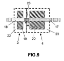
- a blocking region 23 is formed (see Fig. 9 ). This blocking region prevents metal from the metal silicide of one silicidized gate electrode 17 to diffuse to the metal silicide of the other silicidized gate electrode 18 during future temperature steps.
- the blocking region 23 may have the same width as the isolation zone 2.
- the blocking region 23 may have a width w of between 10 nm and 40 nm.
- an increase of the resistivity of the silicide may be caused by implantation of the dopant elements or diffusion retarding species. This may have an effect on electrical performance, e.g. speed, of the devices. Therefore, according to other embodiments of the invention, the width of the blocking region 23 may be different from the width of the isolation zone 2. In these cases, a balance has to be found between blocking and resistivity. This may, for example, be done by adapting the concentration of dopant elements used to form the blocking region.
- implantation of the dopant elements in the silicides may be performed before, after or during silicidation of the gate electrodes 9, 10. Implantation of dopant elements after silicidation of the gate electrodes 9, 10 was described above. In case implantation of dopant elements is performed before silicidation of the gate electrodes 9, 10, implantation may be performed before deposition of the metal layer 16, or in other words directly in the polysilicon 8 of the gate electrodes 9, 10, or may be performed after deposition of the metal layer 16, through this metal layer 16. According to alternative embodiments, dopant elements may already be present in the polysilicon layer that is deposited before the gate electrodes 9, 10 are formed.
- the dopant elements will, because of the lower solubility in the silicide than the metal the silicide is formed of, diffuse towards grain boundaries of the silicide and in that way prevent diffusion of the metal of the silicide from the one to the other silicide.
Landscapes
- Electrodes Of Semiconductors (AREA)
- Metal-Oxide And Bipolar Metal-Oxide Semiconductor Integrated Circuits (AREA)
- Thin Film Transistor (AREA)
- Insulated Gate Type Field-Effect Transistor (AREA)
Priority Applications (5)
| Application Number | Priority Date | Filing Date | Title |
|---|---|---|---|
| AT07012357T ATE499704T1 (de) | 2007-06-25 | 2007-06-25 | Halbleiterbauelement mit gate-elektroden mit unterschiedlicher austrittsarbeit und seine herstellungsmethode |
| EP07012357A EP2009689B1 (de) | 2007-06-25 | 2007-06-25 | Halbleiterbauelement mit Gate-Elektroden mit unterschiedlicher Austrittsarbeit und seine Herstellungsmethode |
| DE602007012676T DE602007012676D1 (de) | 2007-06-25 | 2007-06-25 | Halbleiterbauelement mit Gate-Elektroden mit unterschiedlicher Austrittsarbeit und seine Herstellungsmethode |
| JP2008163157A JP2009038350A (ja) | 2007-06-25 | 2008-06-23 | デュアル仕事関数半導体デバイス |
| US12/145,413 US7851297B2 (en) | 2007-06-25 | 2008-06-24 | Dual workfunction semiconductor device |
Applications Claiming Priority (1)
| Application Number | Priority Date | Filing Date | Title |
|---|---|---|---|
| EP07012357A EP2009689B1 (de) | 2007-06-25 | 2007-06-25 | Halbleiterbauelement mit Gate-Elektroden mit unterschiedlicher Austrittsarbeit und seine Herstellungsmethode |
Publications (2)
| Publication Number | Publication Date |
|---|---|
| EP2009689A1 true EP2009689A1 (de) | 2008-12-31 |
| EP2009689B1 EP2009689B1 (de) | 2011-02-23 |
Family
ID=38457998
Family Applications (1)
| Application Number | Title | Priority Date | Filing Date |
|---|---|---|---|
| EP07012357A Not-in-force EP2009689B1 (de) | 2007-06-25 | 2007-06-25 | Halbleiterbauelement mit Gate-Elektroden mit unterschiedlicher Austrittsarbeit und seine Herstellungsmethode |
Country Status (5)
| Country | Link |
|---|---|
| US (1) | US7851297B2 (de) |
| EP (1) | EP2009689B1 (de) |
| JP (1) | JP2009038350A (de) |
| AT (1) | ATE499704T1 (de) |
| DE (1) | DE602007012676D1 (de) |
Families Citing this family (2)
| Publication number | Priority date | Publication date | Assignee | Title |
|---|---|---|---|---|
| US8084824B2 (en) * | 2008-09-11 | 2011-12-27 | United Microelectronics Corp. | Metal gate transistor and method for fabricating the same |
| US8846474B2 (en) * | 2012-08-20 | 2014-09-30 | Tokyo Electron Limited | Dual workfunction semiconductor devices and methods for forming thereof |
Citations (5)
| Publication number | Priority date | Publication date | Assignee | Title |
|---|---|---|---|---|
| US6864163B1 (en) * | 2002-10-30 | 2005-03-08 | Advanced Micro Devices, Inc. | Fabrication of dual work-function metal gate structure for complementary field effect transistors |
| US20060131652A1 (en) * | 2004-12-20 | 2006-06-22 | Hong-Jyh Li | Transistor device and method of manufacture thereof |
| EP1724818A2 (de) * | 2005-05-16 | 2006-11-22 | Interuniversitair Microelektronica Centrum ( Imec) | Verfahren zur Herstellung vollsilicidierter Dual-Gates und mit diesem Verfahren erhältliche Halbleiterbauelemente |
| EP1724828A2 (de) * | 2005-05-16 | 2006-11-22 | Interuniversitair Microelektronica Centrum ( Imec) | Verfahren zur Herstellung vollsilicidierter Dual-Gates und mit diesem Verfahren erhältliche Halbleiterbauelemente |
| WO2007009846A1 (en) * | 2005-07-21 | 2007-01-25 | Infineon Technologies Ag | Cmos transistors with dual high-k gate dielectric and methods of manufacture thereof |
Family Cites Families (14)
| Publication number | Priority date | Publication date | Assignee | Title |
|---|---|---|---|---|
| US6372557B1 (en) * | 2000-04-19 | 2002-04-16 | Polyfet Rf Devices, Inc. | Method of manufacturing a lateral fet having source contact to substrate with low resistance |
| US7148546B2 (en) * | 2003-09-30 | 2006-12-12 | Texas Instruments Incorporated | MOS transistor gates with doped silicide and methods for making the same |
| US7105889B2 (en) * | 2004-06-04 | 2006-09-12 | International Business Machines Corporation | Selective implementation of barrier layers to achieve threshold voltage control in CMOS device fabrication with high k dielectrics |
| US20060046523A1 (en) * | 2004-08-25 | 2006-03-02 | Jack Kavalieros | Facilitating removal of sacrificial layers to form replacement metal gates |
| JP2006278369A (ja) * | 2005-03-28 | 2006-10-12 | Fujitsu Ltd | 半導体装置の製造方法 |
| JP5015446B2 (ja) * | 2005-05-16 | 2012-08-29 | アイメック | 二重の完全ケイ化ゲートを形成する方法と前記方法によって得られたデバイス |
| WO2006129637A1 (ja) * | 2005-06-01 | 2006-12-07 | Nec Corporation | 半導体装置 |
| JP4784734B2 (ja) * | 2005-09-12 | 2011-10-05 | 日本電気株式会社 | 半導体装置及びその製造方法 |
| JP2007123431A (ja) * | 2005-10-26 | 2007-05-17 | Matsushita Electric Ind Co Ltd | 半導体装置及びその製造方法 |
| JP2007141912A (ja) * | 2005-11-15 | 2007-06-07 | Matsushita Electric Ind Co Ltd | 半導体装置及びその製造方法 |
| JP2007158220A (ja) * | 2005-12-08 | 2007-06-21 | Matsushita Electric Ind Co Ltd | 半導体装置の製造方法 |
| US7911004B2 (en) * | 2006-06-19 | 2011-03-22 | Nec Corporation | Semiconductor device and manufacturing method of the same |
| EP1944801A1 (de) * | 2007-01-10 | 2008-07-16 | Interuniversitair Microelektronica Centrum | Verfahren zur Herstellung einer CMOS-Vorrichtung mit dualer Austrittsarbeit |
| US7416949B1 (en) * | 2007-02-14 | 2008-08-26 | Texas Instruments Incorporated | Fabrication of transistors with a fully silicided gate electrode and channel strain |
-
2007
- 2007-06-25 AT AT07012357T patent/ATE499704T1/de not_active IP Right Cessation
- 2007-06-25 EP EP07012357A patent/EP2009689B1/de not_active Not-in-force
- 2007-06-25 DE DE602007012676T patent/DE602007012676D1/de active Active
-
2008
- 2008-06-23 JP JP2008163157A patent/JP2009038350A/ja active Pending
- 2008-06-24 US US12/145,413 patent/US7851297B2/en not_active Expired - Fee Related
Patent Citations (5)
| Publication number | Priority date | Publication date | Assignee | Title |
|---|---|---|---|---|
| US6864163B1 (en) * | 2002-10-30 | 2005-03-08 | Advanced Micro Devices, Inc. | Fabrication of dual work-function metal gate structure for complementary field effect transistors |
| US20060131652A1 (en) * | 2004-12-20 | 2006-06-22 | Hong-Jyh Li | Transistor device and method of manufacture thereof |
| EP1724818A2 (de) * | 2005-05-16 | 2006-11-22 | Interuniversitair Microelektronica Centrum ( Imec) | Verfahren zur Herstellung vollsilicidierter Dual-Gates und mit diesem Verfahren erhältliche Halbleiterbauelemente |
| EP1724828A2 (de) * | 2005-05-16 | 2006-11-22 | Interuniversitair Microelektronica Centrum ( Imec) | Verfahren zur Herstellung vollsilicidierter Dual-Gates und mit diesem Verfahren erhältliche Halbleiterbauelemente |
| WO2007009846A1 (en) * | 2005-07-21 | 2007-01-25 | Infineon Technologies Ag | Cmos transistors with dual high-k gate dielectric and methods of manufacture thereof |
Also Published As
| Publication number | Publication date |
|---|---|
| US20090020821A1 (en) | 2009-01-22 |
| US7851297B2 (en) | 2010-12-14 |
| ATE499704T1 (de) | 2011-03-15 |
| EP2009689B1 (de) | 2011-02-23 |
| DE602007012676D1 (de) | 2011-04-07 |
| JP2009038350A (ja) | 2009-02-19 |
Similar Documents
| Publication | Publication Date | Title |
|---|---|---|
| US7459752B2 (en) | Ultra thin body fully-depleted SOI MOSFETs | |
| KR101475364B1 (ko) | 반도체 장치 및 반도체 장치의 제조 방법 | |
| US7235472B2 (en) | Method of making fully silicided gate electrode | |
| US6630710B1 (en) | Elevated channel MOSFET | |
| US5960270A (en) | Method for forming an MOS transistor having a metallic gate electrode that is formed after the formation of self-aligned source and drain regions | |
| US8525263B2 (en) | Programmable high-k/metal gate memory device | |
| US6614079B2 (en) | All-in-one disposable/permanent spacer elevated source/drain, self-aligned silicide CMOS | |
| US6096591A (en) | Method of making an IGFET and a protected resistor with reduced processing steps | |
| US6440808B1 (en) | Damascene-gate process for the fabrication of MOSFET devices with minimum poly-gate depletion, silicided source and drain junctions, and low sheet resistance gate-poly | |
| US6864163B1 (en) | Fabrication of dual work-function metal gate structure for complementary field effect transistors | |
| US20040135212A1 (en) | Damascene method for improved mos transistor | |
| US20100038715A1 (en) | Thin body silicon-on-insulator transistor with borderless self-aligned contacts | |
| CN100472756C (zh) | 具有可调栅极功函数的双金属cmos晶体管以及其制法 | |
| JP2005167252A (ja) | 集積回路構造体 | |
| US6987061B2 (en) | Dual salicide process for optimum performance | |
| US6252283B1 (en) | CMOS transistor design for shared N+/P+ electrode with enhanced device performance | |
| US20060170047A1 (en) | Semiconductor device and method of manufacturing the same | |
| US20070194353A1 (en) | Metal source/drain Schottky barrier silicon-on-nothing MOSFET device and method thereof | |
| KR20010023944A (ko) | 반도체장치의 제조방법 | |
| US8759180B2 (en) | Methods for fabricating step gate electrode structures for field-effect transistors | |
| US20040124476A1 (en) | Semiconductor device and method of manufacturing the same | |
| US7851297B2 (en) | Dual workfunction semiconductor device | |
| US6110788A (en) | Surface channel MOS transistors, methods for making the same, and semiconductor devices containing the same | |
| US6586289B1 (en) | Anti-spacer structure for improved gate activation | |
| EP1782466A2 (de) | Doppel-gate-cmos-herstellung |
Legal Events
| Date | Code | Title | Description |
|---|---|---|---|
| PUAI | Public reference made under article 153(3) epc to a published international application that has entered the european phase |
Free format text: ORIGINAL CODE: 0009012 |
|
| 17P | Request for examination filed |
Effective date: 20080618 |
|
| AK | Designated contracting states |
Kind code of ref document: A1 Designated state(s): AT BE BG CH CY CZ DE DK EE ES FI FR GB GR HU IE IS IT LI LT LU LV MC MT NL PL PT RO SE SI SK TR |
|
| AX | Request for extension of the european patent |
Extension state: AL BA HR MK RS |
|
| 17Q | First examination report despatched |
Effective date: 20090408 |
|
| RAP1 | Party data changed (applicant data changed or rights of an application transferred) |
Owner name: IMEC Owner name: PANASONIC CORPORATION |
|
| AKX | Designation fees paid |
Designated state(s): AT BE BG CH CY CZ DE DK EE ES FI FR GB GR HU IE IS IT LI LT LU LV MC MT NL PL PT RO SE SI SK TR |
|
| RTI1 | Title (correction) |
Free format text: SEMICONDUCTOR DEVICE WITH DUAL WORKFUNCTION GATE ELECTRODES AND ITS METHOD OF FABRICATION |
|
| GRAP | Despatch of communication of intention to grant a patent |
Free format text: ORIGINAL CODE: EPIDOSNIGR1 |
|
| GRAS | Grant fee paid |
Free format text: ORIGINAL CODE: EPIDOSNIGR3 |
|
| GRAA | (expected) grant |
Free format text: ORIGINAL CODE: 0009210 |
|
| AK | Designated contracting states |
Kind code of ref document: B1 Designated state(s): AT BE BG CH CY CZ DE DK EE ES FI FR GB GR HU IE IS IT LI LT LU LV MC MT NL PL PT RO SE SI SK TR |
|
| REG | Reference to a national code |
Ref country code: GB Ref legal event code: FG4D |
|
| REG | Reference to a national code |
Ref country code: CH Ref legal event code: EP |
|
| REG | Reference to a national code |
Ref country code: IE Ref legal event code: FG4D |
|
| REF | Corresponds to: |
Ref document number: 602007012676 Country of ref document: DE Date of ref document: 20110407 Kind code of ref document: P |
|
| REG | Reference to a national code |
Ref country code: DE Ref legal event code: R096 Ref document number: 602007012676 Country of ref document: DE Effective date: 20110407 |
|
| REG | Reference to a national code |
Ref country code: NL Ref legal event code: VDEP Effective date: 20110223 |
|
| LTIE | Lt: invalidation of european patent or patent extension |
Effective date: 20110223 |
|
| PG25 | Lapsed in a contracting state [announced via postgrant information from national office to epo] |
Ref country code: LT Free format text: LAPSE BECAUSE OF FAILURE TO SUBMIT A TRANSLATION OF THE DESCRIPTION OR TO PAY THE FEE WITHIN THE PRESCRIBED TIME-LIMIT Effective date: 20110223 Ref country code: LV Free format text: LAPSE BECAUSE OF FAILURE TO SUBMIT A TRANSLATION OF THE DESCRIPTION OR TO PAY THE FEE WITHIN THE PRESCRIBED TIME-LIMIT Effective date: 20110223 Ref country code: SE Free format text: LAPSE BECAUSE OF FAILURE TO SUBMIT A TRANSLATION OF THE DESCRIPTION OR TO PAY THE FEE WITHIN THE PRESCRIBED TIME-LIMIT Effective date: 20110223 Ref country code: PT Free format text: LAPSE BECAUSE OF FAILURE TO SUBMIT A TRANSLATION OF THE DESCRIPTION OR TO PAY THE FEE WITHIN THE PRESCRIBED TIME-LIMIT Effective date: 20110623 Ref country code: GR Free format text: LAPSE BECAUSE OF FAILURE TO SUBMIT A TRANSLATION OF THE DESCRIPTION OR TO PAY THE FEE WITHIN THE PRESCRIBED TIME-LIMIT Effective date: 20110524 Ref country code: ES Free format text: LAPSE BECAUSE OF FAILURE TO SUBMIT A TRANSLATION OF THE DESCRIPTION OR TO PAY THE FEE WITHIN THE PRESCRIBED TIME-LIMIT Effective date: 20110603 |
|
| PG25 | Lapsed in a contracting state [announced via postgrant information from national office to epo] |
Ref country code: BG Free format text: LAPSE BECAUSE OF FAILURE TO SUBMIT A TRANSLATION OF THE DESCRIPTION OR TO PAY THE FEE WITHIN THE PRESCRIBED TIME-LIMIT Effective date: 20110523 Ref country code: NL Free format text: LAPSE BECAUSE OF FAILURE TO SUBMIT A TRANSLATION OF THE DESCRIPTION OR TO PAY THE FEE WITHIN THE PRESCRIBED TIME-LIMIT Effective date: 20110223 Ref country code: SI Free format text: LAPSE BECAUSE OF FAILURE TO SUBMIT A TRANSLATION OF THE DESCRIPTION OR TO PAY THE FEE WITHIN THE PRESCRIBED TIME-LIMIT Effective date: 20110223 Ref country code: CY Free format text: LAPSE BECAUSE OF FAILURE TO SUBMIT A TRANSLATION OF THE DESCRIPTION OR TO PAY THE FEE WITHIN THE PRESCRIBED TIME-LIMIT Effective date: 20110223 Ref country code: FI Free format text: LAPSE BECAUSE OF FAILURE TO SUBMIT A TRANSLATION OF THE DESCRIPTION OR TO PAY THE FEE WITHIN THE PRESCRIBED TIME-LIMIT Effective date: 20110223 Ref country code: BE Free format text: LAPSE BECAUSE OF FAILURE TO SUBMIT A TRANSLATION OF THE DESCRIPTION OR TO PAY THE FEE WITHIN THE PRESCRIBED TIME-LIMIT Effective date: 20110223 Ref country code: AT Free format text: LAPSE BECAUSE OF FAILURE TO SUBMIT A TRANSLATION OF THE DESCRIPTION OR TO PAY THE FEE WITHIN THE PRESCRIBED TIME-LIMIT Effective date: 20110223 |
|
| PG25 | Lapsed in a contracting state [announced via postgrant information from national office to epo] |
Ref country code: DK Free format text: LAPSE BECAUSE OF FAILURE TO SUBMIT A TRANSLATION OF THE DESCRIPTION OR TO PAY THE FEE WITHIN THE PRESCRIBED TIME-LIMIT Effective date: 20110223 Ref country code: EE Free format text: LAPSE BECAUSE OF FAILURE TO SUBMIT A TRANSLATION OF THE DESCRIPTION OR TO PAY THE FEE WITHIN THE PRESCRIBED TIME-LIMIT Effective date: 20110223 |
|
| PG25 | Lapsed in a contracting state [announced via postgrant information from national office to epo] |
Ref country code: SK Free format text: LAPSE BECAUSE OF FAILURE TO SUBMIT A TRANSLATION OF THE DESCRIPTION OR TO PAY THE FEE WITHIN THE PRESCRIBED TIME-LIMIT Effective date: 20110223 Ref country code: RO Free format text: LAPSE BECAUSE OF FAILURE TO SUBMIT A TRANSLATION OF THE DESCRIPTION OR TO PAY THE FEE WITHIN THE PRESCRIBED TIME-LIMIT Effective date: 20110223 Ref country code: CZ Free format text: LAPSE BECAUSE OF FAILURE TO SUBMIT A TRANSLATION OF THE DESCRIPTION OR TO PAY THE FEE WITHIN THE PRESCRIBED TIME-LIMIT Effective date: 20110223 |
|
| PG25 | Lapsed in a contracting state [announced via postgrant information from national office to epo] |
Ref country code: MT Free format text: LAPSE BECAUSE OF FAILURE TO SUBMIT A TRANSLATION OF THE DESCRIPTION OR TO PAY THE FEE WITHIN THE PRESCRIBED TIME-LIMIT Effective date: 20110223 |
|
| PLBE | No opposition filed within time limit |
Free format text: ORIGINAL CODE: 0009261 |
|
| STAA | Information on the status of an ep patent application or granted ep patent |
Free format text: STATUS: NO OPPOSITION FILED WITHIN TIME LIMIT |
|
| REG | Reference to a national code |
Ref country code: CH Ref legal event code: PL |
|
| 26N | No opposition filed |
Effective date: 20111124 |
|
| PG25 | Lapsed in a contracting state [announced via postgrant information from national office to epo] |
Ref country code: PL Free format text: LAPSE BECAUSE OF FAILURE TO SUBMIT A TRANSLATION OF THE DESCRIPTION OR TO PAY THE FEE WITHIN THE PRESCRIBED TIME-LIMIT Effective date: 20110223 |
|
| REG | Reference to a national code |
Ref country code: DE Ref legal event code: R097 Ref document number: 602007012676 Country of ref document: DE Effective date: 20111124 |
|
| REG | Reference to a national code |
Ref country code: IE Ref legal event code: MM4A |
|
| PG25 | Lapsed in a contracting state [announced via postgrant information from national office to epo] |
Ref country code: IE Free format text: LAPSE BECAUSE OF NON-PAYMENT OF DUE FEES Effective date: 20110625 Ref country code: LI Free format text: LAPSE BECAUSE OF NON-PAYMENT OF DUE FEES Effective date: 20110630 Ref country code: CH Free format text: LAPSE BECAUSE OF NON-PAYMENT OF DUE FEES Effective date: 20110630 |
|
| PG25 | Lapsed in a contracting state [announced via postgrant information from national office to epo] |
Ref country code: IT Free format text: LAPSE BECAUSE OF FAILURE TO SUBMIT A TRANSLATION OF THE DESCRIPTION OR TO PAY THE FEE WITHIN THE PRESCRIBED TIME-LIMIT Effective date: 20110223 |
|
| REG | Reference to a national code |
Ref country code: DE Ref legal event code: R082 Ref document number: 602007012676 Country of ref document: DE Representative=s name: MICHALSKI HUETTERMANN & PARTNER PATENTANWAELTE, DE |
|
| REG | Reference to a national code |
Ref country code: GB Ref legal event code: 732E Free format text: REGISTERED BETWEEN 20120705 AND 20120711 |
|
| REG | Reference to a national code |
Ref country code: DE Ref legal event code: R082 Ref document number: 602007012676 Country of ref document: DE Representative=s name: MICHALSKI HUETTERMANN & PARTNER PATENTANWAELTE, DE Effective date: 20120702 Ref country code: DE Ref legal event code: R081 Ref document number: 602007012676 Country of ref document: DE Owner name: IMEC, BE Free format text: FORMER OWNER: IMEC, PANASONIC CORPORATION, , JP Effective date: 20120702 Ref country code: DE Ref legal event code: R081 Ref document number: 602007012676 Country of ref document: DE Owner name: IMEC, BE Free format text: FORMER OWNERS: IMEC, LEUVEN, BE; PANASONIC CORPORATION, KADOMA, OSAKA, JP Effective date: 20120702 |
|
| REG | Reference to a national code |
Ref country code: FR Ref legal event code: TP Owner name: IMEC, BE Effective date: 20120731 |
|
| PG25 | Lapsed in a contracting state [announced via postgrant information from national office to epo] |
Ref country code: MC Free format text: LAPSE BECAUSE OF NON-PAYMENT OF DUE FEES Effective date: 20110630 |
|
| PG25 | Lapsed in a contracting state [announced via postgrant information from national office to epo] |
Ref country code: LU Free format text: LAPSE BECAUSE OF NON-PAYMENT OF DUE FEES Effective date: 20110625 |
|
| PG25 | Lapsed in a contracting state [announced via postgrant information from national office to epo] |
Ref country code: IS Free format text: LAPSE BECAUSE OF FAILURE TO SUBMIT A TRANSLATION OF THE DESCRIPTION OR TO PAY THE FEE WITHIN THE PRESCRIBED TIME-LIMIT Effective date: 20110223 |
|
| PG25 | Lapsed in a contracting state [announced via postgrant information from national office to epo] |
Ref country code: TR Free format text: LAPSE BECAUSE OF FAILURE TO SUBMIT A TRANSLATION OF THE DESCRIPTION OR TO PAY THE FEE WITHIN THE PRESCRIBED TIME-LIMIT Effective date: 20110223 |
|
| PG25 | Lapsed in a contracting state [announced via postgrant information from national office to epo] |
Ref country code: HU Free format text: LAPSE BECAUSE OF FAILURE TO SUBMIT A TRANSLATION OF THE DESCRIPTION OR TO PAY THE FEE WITHIN THE PRESCRIBED TIME-LIMIT Effective date: 20110223 |
|
| REG | Reference to a national code |
Ref country code: FR Ref legal event code: PLFP Year of fee payment: 9 |
|
| PGFP | Annual fee paid to national office [announced via postgrant information from national office to epo] |
Ref country code: GB Payment date: 20150527 Year of fee payment: 9 Ref country code: DE Payment date: 20150521 Year of fee payment: 9 |
|
| PGFP | Annual fee paid to national office [announced via postgrant information from national office to epo] |
Ref country code: FR Payment date: 20150526 Year of fee payment: 9 |
|
| REG | Reference to a national code |
Ref country code: DE Ref legal event code: R119 Ref document number: 602007012676 Country of ref document: DE |
|
| GBPC | Gb: european patent ceased through non-payment of renewal fee |
Effective date: 20160625 |
|
| REG | Reference to a national code |
Ref country code: FR Ref legal event code: ST Effective date: 20170228 |
|
| PG25 | Lapsed in a contracting state [announced via postgrant information from national office to epo] |
Ref country code: FR Free format text: LAPSE BECAUSE OF NON-PAYMENT OF DUE FEES Effective date: 20160630 Ref country code: DE Free format text: LAPSE BECAUSE OF NON-PAYMENT OF DUE FEES Effective date: 20170103 |
|
| PG25 | Lapsed in a contracting state [announced via postgrant information from national office to epo] |
Ref country code: GB Free format text: LAPSE BECAUSE OF NON-PAYMENT OF DUE FEES Effective date: 20160625 |