EP1727000A2 - Appareil de formation d'images avec section pour regler le voltage de developpement et chargement et la quantite d'exposition - Google Patents
Appareil de formation d'images avec section pour regler le voltage de developpement et chargement et la quantite d'exposition Download PDFInfo
- Publication number
- EP1727000A2 EP1727000A2 EP06114469A EP06114469A EP1727000A2 EP 1727000 A2 EP1727000 A2 EP 1727000A2 EP 06114469 A EP06114469 A EP 06114469A EP 06114469 A EP06114469 A EP 06114469A EP 1727000 A2 EP1727000 A2 EP 1727000A2
- Authority
- EP
- European Patent Office
- Prior art keywords
- section
- voltage
- image
- forming apparatus
- image forming
- Prior art date
- Legal status (The legal status is an assumption and is not a legal conclusion. Google has not performed a legal analysis and makes no representation as to the accuracy of the status listed.)
- Withdrawn
Links
- 238000011161 development Methods 0.000 title claims abstract description 105
- 238000012546 transfer Methods 0.000 claims abstract description 39
- 238000010586 diagram Methods 0.000 description 22
- 230000002542 deteriorative effect Effects 0.000 description 8
- 239000000463 material Substances 0.000 description 7
- 238000000034 method Methods 0.000 description 6
- 239000004020 conductor Substances 0.000 description 4
- 230000007423 decrease Effects 0.000 description 4
- 238000001514 detection method Methods 0.000 description 4
- 229910001220 stainless steel Inorganic materials 0.000 description 4
- 239000010935 stainless steel Substances 0.000 description 4
- 238000004140 cleaning Methods 0.000 description 3
- 230000005855 radiation Effects 0.000 description 3
- 238000005096 rolling process Methods 0.000 description 3
- 230000003247 decreasing effect Effects 0.000 description 2
- 238000009826 distribution Methods 0.000 description 2
- 238000012545 processing Methods 0.000 description 2
- 238000002310 reflectometry Methods 0.000 description 2
- 238000012360 testing method Methods 0.000 description 2
- BRLQWZUYTZBJKN-UHFFFAOYSA-N Epichlorohydrin Chemical compound ClCC1CO1 BRLQWZUYTZBJKN-UHFFFAOYSA-N 0.000 description 1
- JOYRKODLDBILNP-UHFFFAOYSA-N Ethyl urethane Chemical compound CCOC(N)=O JOYRKODLDBILNP-UHFFFAOYSA-N 0.000 description 1
- 239000004952 Polyamide Substances 0.000 description 1
- 230000004075 alteration Effects 0.000 description 1
- XAGFODPZIPBFFR-UHFFFAOYSA-N aluminium Chemical compound [Al] XAGFODPZIPBFFR-UHFFFAOYSA-N 0.000 description 1
- 229910052782 aluminium Inorganic materials 0.000 description 1
- 230000015572 biosynthetic process Effects 0.000 description 1
- 230000006866 deterioration Effects 0.000 description 1
- 230000003287 optical effect Effects 0.000 description 1
- 229920002647 polyamide Polymers 0.000 description 1
- 229920001296 polysiloxane Polymers 0.000 description 1
- 239000004065 semiconductor Substances 0.000 description 1
Images





Classifications
-
- G—PHYSICS
- G03—PHOTOGRAPHY; CINEMATOGRAPHY; ANALOGOUS TECHNIQUES USING WAVES OTHER THAN OPTICAL WAVES; ELECTROGRAPHY; HOLOGRAPHY
- G03G—ELECTROGRAPHY; ELECTROPHOTOGRAPHY; MAGNETOGRAPHY
- G03G15/00—Apparatus for electrographic processes using a charge pattern
- G03G15/02—Apparatus for electrographic processes using a charge pattern for laying down a uniform charge, e.g. for sensitising; Corona discharge devices
- G03G15/0283—Arrangements for supplying power to the sensitising device
-
- G—PHYSICS
- G03—PHOTOGRAPHY; CINEMATOGRAPHY; ANALOGOUS TECHNIQUES USING WAVES OTHER THAN OPTICAL WAVES; ELECTROGRAPHY; HOLOGRAPHY
- G03G—ELECTROGRAPHY; ELECTROPHOTOGRAPHY; MAGNETOGRAPHY
- G03G15/00—Apparatus for electrographic processes using a charge pattern
- G03G15/04—Apparatus for electrographic processes using a charge pattern for exposing, i.e. imagewise exposure by optically projecting the original image on a photoconductive recording material
- G03G15/04036—Details of illuminating systems, e.g. lamps, reflectors
- G03G15/04045—Details of illuminating systems, e.g. lamps, reflectors for exposing image information provided otherwise than by directly projecting the original image onto the photoconductive recording material, e.g. digital copiers
-
- G—PHYSICS
- G03—PHOTOGRAPHY; CINEMATOGRAPHY; ANALOGOUS TECHNIQUES USING WAVES OTHER THAN OPTICAL WAVES; ELECTROGRAPHY; HOLOGRAPHY
- G03G—ELECTROGRAPHY; ELECTROPHOTOGRAPHY; MAGNETOGRAPHY
- G03G15/00—Apparatus for electrographic processes using a charge pattern
- G03G15/06—Apparatus for electrographic processes using a charge pattern for developing
- G03G15/065—Arrangements for controlling the potential of the developing electrode
-
- G—PHYSICS
- G03—PHOTOGRAPHY; CINEMATOGRAPHY; ANALOGOUS TECHNIQUES USING WAVES OTHER THAN OPTICAL WAVES; ELECTROGRAPHY; HOLOGRAPHY
- G03G—ELECTROGRAPHY; ELECTROPHOTOGRAPHY; MAGNETOGRAPHY
- G03G2215/00—Apparatus for electrophotographic processes
- G03G2215/04—Arrangements for exposing and producing an image
- G03G2215/0429—Changing or enhancing the image
- G03G2215/0431—Producing a clean non-image area, i.e. avoiding show-around effects
- G03G2215/0465—Developing conditions changed to produce a clean non-image area
Definitions
- the present invention relates to an image forming apparatus such as printer, facsimile machine, Photocopier or MFP (Multi-Function Product) with more than two functions.
- image forming apparatus such as printer, facsimile machine, Photocopier or MFP (Multi-Function Product) with more than two functions.
- image forming apparatus used in an electro photographic system charges the surface of the photosensitive drum evenly, then forms an electrostatic latent image on surface of photosensitive drum through an exposure apparatus, and then develops the electrostatic latent image on the photosensitive drum to form a toner image, finally transfers the toner image on paper through a development apparatus.
- a density of image is usually determined by a quantity of toner transferred on the paper. Nevertheless, because of such factors as the change of operating environment and frequency, there existed circumstances of change in image density. Therefore many methods aimed at prohibiting the change of image density and adjusting the image density into a target level are put forward.
- to charge the photosensitive drum under predetermined charge voltage circumstances to expose with predetermined exposure quantity and to form the electrostatic latent image, to develop the toner into the electrostatic latent image with predetermined development bias voltage, and then to form the test pattern on the photosensitive drum and transfer belt and to detect the density of the test pattern through toner density detecting section.
- To compare the detected value with standard value then to control the image forming circumstances such as, light quantity of exposure apparatus, development bias voltage and toner providing bias voltage, and finally to form the image density at target level on the paper.
- Patent document 1 Japanese patent publication 11-184190 .
- the object of the present invention is to provide an image forming apparatus that prevents the occurrence of fog and gains a more stable image density.
- image forming apparatus comprising:
- the image forming apparatus may further comprise an environment information detecting section to detect environment information in the image forming apparatus; and an environment table to memorize voltage according to the detected environment information, wherein according to the detected print information, a difference between the charge voltage provided to the charging section and the development voltage set by the development voltage setting section is set into a value in predetermined range.
- the environment information may be either of temperature and humidity in the image forming apparatus.
- the image forming apparatus may further comprise a print information detecting section to detect print information; and a temporality setting table to memorize voltage according to the detected print information, wherein according to the detected environment information, a difference between the charge voltage provided to the charging section and the development voltage set by the development voltage setting section is set into a value in predetermined range.
- the print information may be the number of print sheets.
- image forming apparatus comprising:
- the potential detecting section may be to detect a visible image potential on the image carrier.
- the potential detecting section may be to detect a visible image potential on the transfer member.
- the potential detecting section may be to detect a visible image potential on the developing section.
- the potential detecting section is a potential sensor.
- the potential detecting section may be a development electric current detecting circuit.
- the provided image forming apparatus has: image carrier; charging section which provides charge voltage and charges the surface of referred image carrier; exposing section which forms the electrostatic latent image on the surface of referred image carrier; developing section which provides development voltage and makes the developer adhere to the formed electrostatic latent image on the referred image carrier; transferring section which transfers the referred visible image on the transferring components; density detecting section which detects the density of referred visible image on the transferring components; development voltage setting section which sets the developing voltage provided to the referred developing section through the detected density from the referred density detecting section; charging voltage setting section which sets the potential difference within predetermined range between charging voltage that provides for referred charging section and the referred predetermined developing voltage; exposure quantity section which sets the referred predetermined charging voltage and exposure quantity. Therefore, outputting images with a stable density and good quality but out of fog could be gained.
- the provided image forming apparatus has: image carrier; charging section which provides charge voltage and charge the surface of referred image carrier; exposure section which forms the electrostatic latent image on the surface of referred image carrier; developing section which provides development voltage and makes the developer adhere to the formed electrostatic latent image on the referred image carrier; transferring section which transfers the referred visible image on the transferring components; density detecting section which detects the density of referred visible image on the transferring components; development voltage setting section which sets the developing voltage provided to the referred developing section through the detected density from the referred density detecting section; charging voltage setting section which sets the potential difference within predetermined range between charging voltage that provides for referred charging section and the referred predetermined developing voltage; exposure quantity section which sets the referred predetermined charging voltage and exposure quantity. Therefore, outputting images with a stable density and good quality but out of fog could be gained.
- non-image section contrast voltage it is the absolute value for the difference between the result of adding development bias voltage to toner layer potential and the photosensitive drum charge potential; Furthermore, development contrast voltage is the absolute value for the difference between the result of adding the development bias voltage to the toner layer potential and the latent image potential of exposure section;
- Fig 4 is an environment level chart stepwisely showing the image forming characteristics according to temperature and humidity in the present invention.
- high temperature and humidity environment of 30 degree and 80% humidity is known as level 1
- the indoor environment of 25 degree and 45% humidity is known as level 3
- the low temperature and humidity environment of 10 degree and 10% humidity is known as level 6.
- charge environment table voltage is an amendment voltage set within the charge environment table and used in different operation environments. As described later in the text, the charge environment voltage is predetermined corresponding to various operation environments of the image forming apparatus for the purpose of changing the non-image section contrast voltage value into predetermined range.
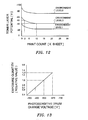
- Charge temporality table voltage is set within the charge temporality table, that is, a kind of voltage based on the changing features of toner layer potential of print count showed in Fig 12 and used to predetermine the changing quantity of toner potential showed in Fig 6 as well. For example, when the environment level value is 3, print count is 2000 and charge environment table voltage is -700V (Fig 5), the charge temporality table voltage value is +10 V (Fig 6).
- Fig. 9 is a diagram showing the relation between charge bias voltage and fog degree when development bias voltage (V db) is -300V and the environment level is 1 and 3 at print initial stage.
- the charge bias voltage is set as -900V, the changing tendency of the non-image section contrast voltage for environment levels 1 and 3 is observed.
- the environment level is 1, the photosensitive drum charge voltage is -500V; when the environment level is 3, the photosensitive drum charge voltage is -400V.
- the toner layer potential is -40V when the environment level is 1; and the toner layer potential is -60V when the environment level is 3.
- the non-image section contrast voltage is
- 160V; when the environment level is 3,
- 40V.
- Fig 9 when charge bias voltage is predetermined as -900V, environment level is 1; the fog value is below 0.5 that turned out to be good. By contrast, when the environment level is 3, the fog value is 2.0 that turned out to be poor. In other words, when the non-image section contrast voltage decreases from 160 V to 40 V, fog value change from good condition under 0.5 to deteriorating poor condition of 2.0. That is, the decrease of non-image section contrast voltage leads to the tendency of fog deteriorating. Actually, in Fig 9, with regards to the curve of environment level 1, the good condition of charge bias voltage should be between the range of -840 V to -920, as a result, the range of non-image section contrast voltage can be calculated.
- the charge bias voltage is known as ⁇ 840 V and ⁇ 920 V
- the corresponding photosensitive drum charge potential is ⁇ 460 V and ⁇ 540 V according to Fig 10. It can be referred that the non-image section contrast voltage increases from
- 100V to
- 180V.
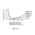
- Fig. 15 is a diagram showing the change relation between non-image section contrast voltage and fog degree. According to the drawings, among different operation environments, if the non-image section contrast voltage value is controlled within the range of 100V-180V and fog value is under 0.5, the fine image quality can be gained.
- the feature of the present invention is to regard the non-image section contrast voltage as a predetermined value that is used to control bias conditions. (The range value is 100 V to 180 V according to Fig 15). Furthermore, the exposure quantity is adjusted according to the change of charge bias voltage in order to prevent the happening of fog. As a result, a more stable image density can be gained. Two embodiments are explained.
- environment voltage table is set for purpose of making the non-image section contrast voltage into predetermined value range.
- the present embodiment is an example of image density amendment in which the image density changes according to the characteristic changes of such factors as actual operation environment, print count, operation frequency, print image area rate or the image forming process material.
- the non-image section contrast voltage makes the fog value being voltage value under 0.5 under different operation environments.
- the present embodiment is composed of two great parts, say, (1) and (2). (1) Firstly, in order to make the non-image section contrast voltage become the value within the predetermined range (here with a range of 100V-180V), the voltage value is set in the charge environment table and makes the image forming apparatus work with gained bias conditions.
- Fig. 1 is a diagram of an image forming apparatus according to embodiment 1 of the present invention.
- the image forming apparatus is a printer of electronic photographic.
- a photoconductor layer is formed on a drum-like conductor's surface made of aluminum so as to form a photosensitive drum 1 as an image carrier by revolvingly driven.
- a charging roller 2; an exposure head 3; a developing machine 4; a transfer belt 9; a photosensitive drum cleaning blade 10; a fixing machine 11 and a density sensor 13 are equipped.
- the charging roller 2 is an electroconductive elastic body made of conductors such as stainless steel with its axis wrapped with epichlorohydrin outside. It is installed at the position attaching to the photosensitive drum.
- the exposure head 3, for example, is composed of LED components and lens array .It is equipped at the position where the shining light came out of the LED components which form image on the surface of the photosensitive drum.
- the developing machine 4 is composed of developing roller 5, providing roller 6, and adjustment blade 7.
- the developing roller 5 is an electroconductive elastic body made of conductors such as stainless steel with its axis wrapped with urethane outside.
- the providing roller 6 is an elastic body of foam-ability made of conductors such as stainless steel with its axis wrapped with silicone outside.
- the ajustment blade 7 is made of tabular material such as stainless steel. Internally, there also existed toner cartridge that provides toner while not displayed on drawings.
- the developing roller 5 is installed at the position attached to photosensitive drum 1.
- the transfer belt 9 is made of banding material of semiconductor such as polyamide and is installed at the position attached to photosensitive drum 1.
- a transfer roller 8 made of elastic body of formability is installed at its corresponding position.
- the density sensor 13 is a photo sensor composed of illuminating and light receiving diode. It is installed at the backward position between transfer belt 9 and photosensitive drum 1.
- the transfer cleaning blade 14 is installed at the position attached to transfer belt. 12 is used to denote the print medium transmit on transfer belt 9.
- the environment sensor 20 is included in the image forming apparatus to detect temperature and humidity of such apparatus.
- Fig. 2 is a controlling block diagram of an image forming apparatus according to embodiment 1 of the present invention.
- Charge bias voltage controlling section 21 is connected to charging roller 2 and provides it with charge bias voltage set by calculation section 24.
- Development bias voltage controlling section 22 is connected to developing roller 5 and provides it with development bias voltage set by calculation section 24.
- Exposure quantity controlling section 23 is connected to exposure head 3 and provides it driving current value set by calculating section 24.
- Density sensor 13 detects the toner image on transfer belt 9. The output value is the detected density calculated by calculating section 24.
- Environment sensor 20 detects the internal temperature and humidity of the apparatus.
- the output value is known as the detected environment level value calculated by the calculation section 24.
- a print count section 25 is installed in the calculating section 24 to detect the rolling count for photosensitive drum 1 and calculates the count value corresponding to print count by calculation.
- memorizing section 26 is connected to the calculating section 24.
- the charge environment table 27 including voltage value corresponding to environment level value is installed; charge temporality table controlling section 28 memorizing voltage value corresponding to print count; in addition, exposure adjustment standard table 29 memorizing voltage value corresponding to environment level value.
- Fig. 3 is a flowchart of density amendment according to embodiment 1 of the present invention. Firstly, from the charge environment table 27 memorized by memorizing section 26, the charge environment table voltage value is read corresponding to environment level value. From the charge temporality table voltage value controlling section 28 memorized by the same memorizing section 26, the charge temporality table voltage value is read corresponding to the print count value. Then, by adding the charge environment table voltage value to the charge temporality table voltage value to calculate charge standard voltage. The charge environment table voltage value sets the non-image section contrast voltage value (100V to 180V) (step S31) within predetermined range under different operation environment levels. Then, by adding the calculated charge standard voltage to development contrast voltage to calculate charge anti-bias voltage (step S32).
- step S33 the toner image is created on the photosensitive drum according to the appointed charge bias voltage, development bias voltage and exposure quantity. Toner image is related to the position of density sensor 13, for example: if the patch patterns with image area rate of 100%, 70%, and 30% is acceptable (step S34).
- the formed toner image is directly transferred on the transfer belt, then when the patch pattern moves below the density sensor 13, the reflectivity of patch pattern is read through the rolling of transfer belt 9 which is used for calculation in the calculating section 24 to detect image density (step S35).
- the difference between detected density value and target value is calculated after the calculation of image density in the calculating section 24.
- the amended voltage value of development bias voltage corresponding to amended difference density is calculated according to the amended coefficient memorized in memorization section 26 in advance. (Step S36).
- Step S37 By adding the amended value of development bias voltage to development bias voltage value according to the density calculated above to calculate the amended development bias voltage.
- step S38 By adding the charge standard voltage to the amended development bias voltage after the amended development bias voltage is calculated to calculate the amended charge bias voltage (step S38). By multiplying the difference between exposure quantity adjustment table value and amended charge bias voltage with adjustment coefficient after the amended charge bias voltage is calculated to calculate the exposure quantity adjustment value (step S39). This flow procedure is completed after the exposure quantity is adjusted.
- the environment level value of image forming apparatus is 3, print count 2000.
- Fig. 5 is a chart showing charge environment table voltage corresponding to environment level according to embodiment 1 of this invention.
- Fig. 6 is a chart showing charge temporality table voltage corresponding to print count according to embodiment 1 of this invention.
- step S33 Since the exposure quantity adjustment standard voltage is -500V when the environment level is 3, the charge bias voltage being -1000V as described before, the difference is changed into -500V.
- the development bias voltage is described as -310V and the toner layer potential Vt1 is -50V according to Fig. 12 (print count is 2000). According to all the figures, the development contrast voltage is
- 260V. Non-image section contrast voltage Vdc is
- 140V. According to Fig. 15, fog value is 0.5 that proved to be good.
- the density is detected.
- the detected density OD (Optical Density) is 1.29 and the target density OD is 1.5.
- the amended coefficient is 0.3 corresponding to the OD changing quantity when the changing quantity of development bias voltage is 100V
- the latent image potential on the photosensitive drum referred in Fig. 14C since the charge potential of photosensitive drum is increased, the all the latent image potential are increased to -70V. Therefore, the non-image section contrast voltage Vdc3 is
- 140V, according to Fig. 15, the fog is below the range of 0.5 that proved to be good.
- the amended density gained after the development contrast voltage Vdc3 is decreased
- 260V. The exposure quantity must be adjusted before the amended density is gained.
- exposure quantity adjustment standard table value is -500V
- the amended charge bias voltage is -1070V
- the difference is -570V
- the amended value of exposure quantity is 1.21.
- the non-image section contrast voltage Vdc4 is kept as 140V; furthermore since the development contrast voltage Vdc4 is 330V, the latent image potential of exposure section is -100V, as a result the target density is 1.5.
- the bias control is completed through the density amendment of the present embodiment.
- the non-image section contrast voltage is usually within the predetermined range under the circumstances of change of development bias voltage and operation environments.
- the non-image section contrast voltage is 140V. Therefore, as showed in Fig. 15, good print quality with fog value below 0.5 can be gained under all environment levels. If the fog value below 0.5 is regarded as target, the setting value of non-image section contrast voltage is good as long as being within the range of 100V and 180V.
- the non-image section contrast voltage when the charge bias voltage is changed, a certain degree of density could be reached since the exposure quantity is adjusted according to that changing quantity and the development contrast voltage is kept as the amended density value.
- the way of adjustment of driving current related to exposure quantity is specified. Nevertheless, since the exposure quantity is proportion to radiation quantity and radiation time corresponding to driving current, the radiation time also can be adjusted when the driving current is at a certain level.
- the density amendment as referred above can be performed when the power of the apparatus is turned on, print count is defined into a certain amount or the environment level is changed.
- the value showed in the present embodiment is only one example that meets the conditions for characteristics of usage craft materials and craftwork speed.
- the table voltage value is set into most suitable one that turned out to be good.
- the present embodiment is an example amend density in which the photosensitive drum charge potential and toner layer potential is directly detected, the non-image section contrast voltage value is set into predetermined range (here is 100V-180V) to amend density through the adjustment of the non-image section contrast voltage in different operation environments of image forming apparatus.
- the image density of image apparatus with operation is detected and the difference between target density value and it is calculated.
- the bias voltage condition is amended according to the density value difference.
- the standard bias voltage is calculated when the non-image section contrast voltage value is regarded as target non-image section contrast voltage value under amended bias voltage, then the target density is gained according to the adjustment of exposure quantity.
- the target non-image section contrast voltage value is set into a range in which the fog value is below 0.5 in different operation environment.
- Fig. 16 is a diagram of an image forming apparatus according to embodiment 2 of this invention. Since the electronic photographic printer as an image forming apparatus, the present embodiment provides the same serial numbers and omits the specification when it enjoys the same structure as that of embodiment 1.
- potential sensor 51 is set in the positions where it connects with developing roller and transfer belt 9 by facing to the photosensitive drum 1.
- the potential sensor 51 is a non-contact type surface potential sensor.
- the printing process of the image forming apparatus of the present embodiment is nearly the same as that of embodiment 2.
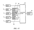
- Fig. 17 is a control block diagram of an image forming apparatus according to embodiment 2 of this invention.
- the charge bias voltage controlling section is connected to charging roller 2 and provides it with the charge bias voltage set by calculating section 52.
- the development bias voltage controlling section 22 is connected to developing roller 5 and provides it with the development bias voltage set by calculating section 52.
- the exposure quantity controlling section is connected to exposure head 3 and provides it with the driving current set by calculating section 52.
- the density sensor 13 reads the toner image on transfer belt and the detected output value is the density calculated by calculating section 52.
- the potential sensor 51 reads the photosensitive drum charge potential and toner layer potential formed on the photosensitive drum and the detected output value is the voltage value calculated by calculating section 52.
- Memorizing section is connected to calculating section 52.
- Fig. 18 is a flowchart of density amendment according to embodiment 2 of this invention.
- the standard charge bias voltage memorized by memorizing section 53 is read and supply charging roller voltage charge the surface of the photosensitive drum.
- the photosensitive drum charge potential is detected by potential sensor 51.
- the standard charge bias voltage is -1000V; the detected photosensitive drum charge voltage is -520V.
- the detected photosensitive drum charge potential is memorized into memorizing section 53.
- the standard exposure quantity memorized in memorizing section 53 is read.
- the driving current corresponding to standard exposure quantity is provided to the exposure head 3 and the electrostatic latent image pattern is formed.
- the standard development bias voltage value memorized in memorizing section 53 is read and provided to developing roller 5 which develops the electrostatic latent image pattern and changes into toner image (Step S 62). If the driving current of standard exposure quantity is 3 mA, the standard development bias voltage is -300V. It is hoped that the electrostatic latent image pattern can be used in detecting toner layer potential and density. For example, the patch patterns with area rate of 100%, 70% and 30% are formed corresponding to the positions of potential sensor 51 and density sensor 13.
- Step S 63 the surface voltage of amended pattern with an area rate of 100% of toner image formed on photosensitive drum is detected by potential sensor 51 and calculated in calculating section 52 leading to the detection of toner layer potential.
- the detected toner layer potential is memorized into memorizing section 53. In this case the detected toner layer potential is -80V.
- the toner image formed on the photosensitive drum is directly transferred on transfer belt.
- the patch pattern moves below the density sensor 13, the reflectivity of patch pattern is read by diode through the rolling of transfer belt 9 that is used for calculation in the calculating section 52 (step 64).
- the toner transfer on transfer belt 9 by density sensor 13 is wiped fall by cleaning blade and is recycled into toner cartridges that do not display on pattern.
- the difference between density value and target value detected by calculating section 52 is calculated.
- the amended voltage value of development bias voltage corresponding to amended difference density is calculated according to the amended coefficient memorized in memorization section 53 in advance (Step 65).
- the amended coefficient is 0.3 corresponding to the OD changing quantity when the changing quantity of development bias voltage is 100V.
- the development bias voltage proves to be good after the decreasing of 100V.
- the development bias amended voltage value corresponding to density is +100V.
- step S67 After the calculation of amended development bias voltage, by subtracting the detected toner layer potential value and the amended development bias voltage memorized in memorizing section 53 from the detected photosensitive drum charge potential value memorized in the same memorizing section to calculate the non-image section contrast voltage (step S67).
- the detected photosensitive drum charge potential value is -520V
- the detected toner layer potential value is -80V
- the amended development bias voltage is -200V
- the non-image section contrast voltage is
- 240V. Since the non-image section contrast voltage is above 180V, the fog value above 0.5 is viewed as within the poor range according to Fig. 15.
- the target contrast voltage is set into the range that makes the fog value be under 0.5.
- the amended charge bias voltage is provided to charging roller that charges photosensitive drum 1. Furthermore, the current charge potential is detected by potential sensor 51 (step S69). In this case, the detected photosensitive drum charge potential is -410V. As referred above, since the amended development bias voltage is -200V, the detected toner layer potential value is -80V and, the non-image section contrast voltage is
- 130 V. The fog value is below 0.5 according to Fig. 15.
- the exposure quantity adjustment value is calculated with the detected charge voltage value (step S70).
- the desired image density can be gained through density amendment after the adjustment of latent potential depth.
- the bias control can be completed through density amendment in the present embodiment.
- the density amendment of the present embodiment since the non-image section contrast voltage is adjusted after the direct detection of photosensitive drum charge potential and toner layer potential value, the non-image section contrast voltage is usually within the predetermined range under the circumstances of change of development bias voltage, toner layer potential and operation environments. Therefore, good print quality with fog value below 0.5 can be gained under all environment levels. If the fog value below 0.5 is regarded as target, the setting value of non-image section contrast voltage is good as long as it being within the range of 100V and 180V. (See Fig. 15). In addition, for the purpose of setting the non-image section contrast voltage, when the charge bias voltage is changed, a certain degree of density could be reached since the exposure quantity is adjusted according to that changing quantity and the development contrast voltage is kept as the amended density value.
- the density amendment as referred above can be performed when the power of the apparatus is turned on, print count is defined into a certain amount or the environment level is changed.
- the value showed in the present embodiment is only one example that meets the conditions for characteristics of usage craft materials and craftwork speed.
- the target value is set into most suitable one that turned out to be good. Therefore, the decision range of the quality for non-image section contrast voltage can be made according to the corresponding required quality level.
- the present invention not only can be applied in monochrome printer with one developing machine, but color printer with four developing machines that transfers with one cycle, let alone color printer with four cycles that forms colorful images transferred one by one for four times repeatedly with middle transfer belt.
- the potential sensor can also be set on the opposite position of transfer belt to detect and control the toner layer potential after transferring.
- the potential sensor can also be set on the opposite position of developing roller to detect and control the toner layer potential on the developing roller.
- the current detecting circuit as a replacement for potential sensor, can be used to detect the current on the developing roller.
- the detected current value can be applied in calculating the toner layer and photosensitive drum charge potential that can be used in controlling process.
Landscapes
- Physics & Mathematics (AREA)
- General Physics & Mathematics (AREA)
- Engineering & Computer Science (AREA)
- Plasma & Fusion (AREA)
- Control Or Security For Electrophotography (AREA)
- Developing For Electrophotography (AREA)
- Exposure Or Original Feeding In Electrophotography (AREA)
- Electrostatic Charge, Transfer And Separation In Electrography (AREA)
Applications Claiming Priority (1)
| Application Number | Priority Date | Filing Date | Title |
|---|---|---|---|
| JP2005151345A JP4953588B2 (ja) | 2005-05-24 | 2005-05-24 | 画像形成装置 |
Publications (2)
| Publication Number | Publication Date |
|---|---|
| EP1727000A2 true EP1727000A2 (fr) | 2006-11-29 |
| EP1727000A3 EP1727000A3 (fr) | 2013-10-02 |
Family
ID=36888789
Family Applications (1)
| Application Number | Title | Priority Date | Filing Date |
|---|---|---|---|
| EP06114469.7A Withdrawn EP1727000A3 (fr) | 2005-05-24 | 2006-05-24 | Appareil de formation d'images avec section pour regler le voltage de developpement et chargement et la quantite d'exposition |
Country Status (4)
| Country | Link |
|---|---|
| US (1) | US7539429B2 (fr) |
| EP (1) | EP1727000A3 (fr) |
| JP (1) | JP4953588B2 (fr) |
| CN (1) | CN100595685C (fr) |
Cited By (3)
| Publication number | Priority date | Publication date | Assignee | Title |
|---|---|---|---|---|
| EP2966505A1 (fr) * | 2014-07-07 | 2016-01-13 | Ricoh Company, Ltd. | Appareil de formation d'image |
| JP2020082654A (ja) * | 2018-11-30 | 2020-06-04 | 株式会社沖データ | 画像形成装置 |
| EP4286949A1 (fr) * | 2022-05-30 | 2023-12-06 | Ricoh Company, Ltd. | Appareil de formation d'images |
Families Citing this family (25)
| Publication number | Priority date | Publication date | Assignee | Title |
|---|---|---|---|---|
| US7751170B2 (en) * | 2006-06-02 | 2010-07-06 | The Board Of Trustees Of The Leland Stanford Junior University | Charge management of electrically isolated objects via modulated photoelectric charge transfer |
| JP5354843B2 (ja) * | 2006-06-05 | 2013-11-27 | キヤノン株式会社 | 画像形成装置 |
| JP5105142B2 (ja) * | 2006-11-21 | 2012-12-19 | 富士ゼロックス株式会社 | 画像形成装置及びプログラム |
| JP5064833B2 (ja) * | 2007-02-23 | 2012-10-31 | キヤノン株式会社 | 画像形成装置 |
| JP4586870B2 (ja) * | 2008-03-14 | 2010-11-24 | コニカミノルタビジネステクノロジーズ株式会社 | 画像形成装置 |
| JP5338219B2 (ja) * | 2008-09-19 | 2013-11-13 | コニカミノルタ株式会社 | 画像形成装置 |
| DE102008056966B4 (de) * | 2008-11-11 | 2016-06-02 | Océ Printing Systems GmbH & Co. KG | Verfahren und Anordnung zur Regelung der Tonereinfärbung von Ladungsbildern auf einem Fotoleiterelement bei einem elektrografischen Druckgerät |
| US7890005B2 (en) * | 2009-01-07 | 2011-02-15 | Infoprint Solutions Company, Llc | Adjusting electrostatic charges used in a laser printer |
| JP5198306B2 (ja) * | 2009-02-05 | 2013-05-15 | 京セラドキュメントソリューションズ株式会社 | 画像形成装置 |
| JP5615004B2 (ja) * | 2010-03-05 | 2014-10-29 | キヤノン株式会社 | 高圧制御装置、画像形成装置及び高電圧出力装置 |
| JP4995331B2 (ja) * | 2010-05-17 | 2012-08-08 | キヤノン株式会社 | 画像形成装置 |
| JP5729927B2 (ja) * | 2010-06-30 | 2015-06-03 | キヤノン株式会社 | 画像形成装置及び高圧制御装置 |
| JP5382082B2 (ja) * | 2011-09-29 | 2014-01-08 | ブラザー工業株式会社 | 画像形成装置および露光量の設定方法 |
| JP5854846B2 (ja) * | 2012-01-10 | 2016-02-09 | キヤノン株式会社 | 画像形成装置 |
| JP2013250302A (ja) * | 2012-05-30 | 2013-12-12 | Kyocera Document Solutions Inc | 高圧電源装置及び画像形成装置 |
| JP6176906B2 (ja) * | 2012-09-11 | 2017-08-09 | キヤノン株式会社 | 画像形成装置 |
| JP6029455B2 (ja) * | 2012-12-21 | 2016-11-24 | キヤノン株式会社 | 画像形成装置 |
| JP2014128909A (ja) * | 2012-12-28 | 2014-07-10 | Toshiba Corp | 画像形成装置 |
| JP5855063B2 (ja) * | 2013-09-19 | 2016-02-09 | キヤノン株式会社 | 画像形成装置 |
| JP6244828B2 (ja) * | 2013-11-06 | 2017-12-13 | 株式会社リコー | 画像形成装置 |
| JP6641634B2 (ja) * | 2016-03-18 | 2020-02-05 | 株式会社リコー | 画像形成装置及び画像形成方法 |
| JP2017187627A (ja) * | 2016-04-06 | 2017-10-12 | キヤノン株式会社 | 画像形成装置 |
| JP6880636B2 (ja) * | 2016-10-13 | 2021-06-02 | ブラザー工業株式会社 | 画像形成装置および画像形成方法 |
| JP2018132723A (ja) * | 2017-02-17 | 2018-08-23 | 株式会社リコー | 画像形成システム、画像形成方法、及び画像形成プログラム |
| JP7762042B2 (ja) * | 2021-11-11 | 2025-10-29 | キヤノン株式会社 | 画像形成装置 |
Citations (7)
| Publication number | Priority date | Publication date | Assignee | Title |
|---|---|---|---|---|
| US5305057A (en) | 1991-07-05 | 1994-04-19 | Minolta Camera Kabushiki Kaisha | Image forming apparatus having correction means for modifying image density signals according to a gradation correction table |
| JPH0798526A (ja) | 1993-09-29 | 1995-04-11 | Fuji Xerox Co Ltd | 画像形成装置 |
| JPH11184190A (ja) | 1997-12-24 | 1999-07-09 | Oki Data Corp | 電子写真式プリンタ |
| US6125245A (en) * | 1998-04-09 | 2000-09-26 | Canon Kabushiki Kaisha | Image forming apparatus |
| JP2001183876A (ja) | 1999-12-24 | 2001-07-06 | Fuji Xerox Co Ltd | 画像形成装置 |
| US20010043815A1 (en) | 2000-03-29 | 2001-11-22 | Kenichiro Kitajima | Image forming apparatus which corrects image forming conditions in low-temperature environment and at continuous image formation |
| US20040175195A1 (en) | 2003-03-07 | 2004-09-09 | Toshiba Tec Kabushiki Kaisha | Image forming apparatus and image forming method |
Family Cites Families (15)
| Publication number | Priority date | Publication date | Assignee | Title |
|---|---|---|---|---|
| JP3013441B2 (ja) * | 1990-11-30 | 2000-02-28 | ミノルタ株式会社 | デジタル画像形成装置 |
| US5315351A (en) * | 1991-04-08 | 1994-05-24 | Minolta Camera Kabushiki Kaisha | Image forming apparatus |
| JPH063911A (ja) * | 1992-06-19 | 1994-01-14 | Canon Inc | 画像形成装置 |
| JPH0792749A (ja) * | 1993-09-21 | 1995-04-07 | Toshiba Corp | 画像形成装置並びに画像形成方法 |
| JPH0916039A (ja) * | 1995-06-30 | 1997-01-17 | Minolta Co Ltd | 画像形成装置 |
| JPH09179382A (ja) * | 1995-12-22 | 1997-07-11 | Toshiba Corp | 画像形成装置 |
| JPH1048894A (ja) * | 1996-07-29 | 1998-02-20 | Nec Data Terminal Ltd | 画像形成装置 |
| JP3479446B2 (ja) * | 1998-01-29 | 2003-12-15 | シャープ株式会社 | 画像形成装置の画質補償装置 |
| JP3594841B2 (ja) * | 1999-07-07 | 2004-12-02 | シャープ株式会社 | 画像形成装置 |
| JP2001092200A (ja) * | 1999-09-22 | 2001-04-06 | Toshiba Tec Corp | 画像形成装置 |
| JP2002040725A (ja) * | 2000-07-24 | 2002-02-06 | Ricoh Co Ltd | 画像形成装置 |
| JP4643076B2 (ja) * | 2001-09-03 | 2011-03-02 | 株式会社ヒラノテクシード | ロール支持装置 |
| CN1295571C (zh) * | 2002-02-20 | 2007-01-17 | 精工爱普生株式会社 | 图像形成装置及图像形成方法 |
| JP4396152B2 (ja) * | 2002-08-06 | 2010-01-13 | セイコーエプソン株式会社 | 画像形成装置および画像形成方法 |
| JP4337323B2 (ja) * | 2002-10-04 | 2009-09-30 | セイコーエプソン株式会社 | 画像形成装置および画像形成方法 |
-
2005
- 2005-05-24 JP JP2005151345A patent/JP4953588B2/ja not_active Expired - Fee Related
-
2006
- 2006-05-23 CN CN200610084108.9A patent/CN100595685C/zh active Active
- 2006-05-23 US US11/438,352 patent/US7539429B2/en active Active
- 2006-05-24 EP EP06114469.7A patent/EP1727000A3/fr not_active Withdrawn
Patent Citations (7)
| Publication number | Priority date | Publication date | Assignee | Title |
|---|---|---|---|---|
| US5305057A (en) | 1991-07-05 | 1994-04-19 | Minolta Camera Kabushiki Kaisha | Image forming apparatus having correction means for modifying image density signals according to a gradation correction table |
| JPH0798526A (ja) | 1993-09-29 | 1995-04-11 | Fuji Xerox Co Ltd | 画像形成装置 |
| JPH11184190A (ja) | 1997-12-24 | 1999-07-09 | Oki Data Corp | 電子写真式プリンタ |
| US6125245A (en) * | 1998-04-09 | 2000-09-26 | Canon Kabushiki Kaisha | Image forming apparatus |
| JP2001183876A (ja) | 1999-12-24 | 2001-07-06 | Fuji Xerox Co Ltd | 画像形成装置 |
| US20010043815A1 (en) | 2000-03-29 | 2001-11-22 | Kenichiro Kitajima | Image forming apparatus which corrects image forming conditions in low-temperature environment and at continuous image formation |
| US20040175195A1 (en) | 2003-03-07 | 2004-09-09 | Toshiba Tec Kabushiki Kaisha | Image forming apparatus and image forming method |
Cited By (5)
| Publication number | Priority date | Publication date | Assignee | Title |
|---|---|---|---|---|
| EP2966505A1 (fr) * | 2014-07-07 | 2016-01-13 | Ricoh Company, Ltd. | Appareil de formation d'image |
| US9304489B2 (en) | 2014-07-07 | 2016-04-05 | Ricoh Company, Limited | Image forming apparatus |
| JP2020082654A (ja) * | 2018-11-30 | 2020-06-04 | 株式会社沖データ | 画像形成装置 |
| EP4286949A1 (fr) * | 2022-05-30 | 2023-12-06 | Ricoh Company, Ltd. | Appareil de formation d'images |
| US12189319B2 (en) | 2022-05-30 | 2025-01-07 | Ricoh Company, Ltd. | Image forming apparatus to perform phase matching control to match phases of image-density cycle fluctuations |
Also Published As
| Publication number | Publication date |
|---|---|
| CN100595685C (zh) | 2010-03-24 |
| US20060269306A1 (en) | 2006-11-30 |
| EP1727000A3 (fr) | 2013-10-02 |
| US7539429B2 (en) | 2009-05-26 |
| JP2006330188A (ja) | 2006-12-07 |
| JP4953588B2 (ja) | 2012-06-13 |
| CN1869830A (zh) | 2006-11-29 |
Similar Documents
| Publication | Publication Date | Title |
|---|---|---|
| EP1727000A2 (fr) | Appareil de formation d'images avec section pour regler le voltage de developpement et chargement et la quantite d'exposition | |
| US5250988A (en) | Electrophotographic apparatus having image control means | |
| EP0338962A2 (fr) | Méthode et appareil de contrôle des paramètres électrostatiques d'un dispositif de reproduction électrophotographique | |
| US6686943B2 (en) | Control method of an electrophotographic record apparatus and image formation apparatus including controlling developing bias and photoconductor surface potential | |
| US7672603B2 (en) | Image formation control based on printing rate | |
| JP2006301461A (ja) | 画像形成装置 | |
| US7539428B2 (en) | Image-forming device wherein the density of the images are corrected | |
| US10197939B2 (en) | Image forming apparatus with a control that compensates for changing humidity | |
| US6501917B1 (en) | Method and apparatus for image forming capable of effectively performing image density adjustment | |
| US7873289B2 (en) | Image forming apparatus and method to control a velocity ratio thereof | |
| US7715741B2 (en) | Image forming apparatus with a toner image density feature and related method | |
| JP2016161618A (ja) | 画像形成装置およびこれに用いられるプロセスカートリッジ | |
| US6750893B2 (en) | Image forming apparatus and method controlling a laser scan unit | |
| US7254349B2 (en) | Image forming apparatus having means to control condition of current supply to discharge wire and grid of charging member | |
| JP7588995B2 (ja) | 画像形成装置 | |
| KR100193828B1 (ko) | 전자사진 현상방식을 채용한 화상형성장치의 화상농도 조정장치 | |
| US20200183315A1 (en) | Image forming apparatus, deterioration state detection method and non-transitory computer-readable recording medium encoded with deterioration state detection program | |
| US6510293B1 (en) | Image forming apparatus having toner density detection and image density control method therefore | |
| JP4260085B2 (ja) | 現像濃度調節装置,画像形成装置 | |
| JP7810005B2 (ja) | 画像形成装置及び画像形成装置の制御方法 | |
| JP2001255711A (ja) | 画像形成装置 | |
| US20240419097A1 (en) | Image forming apparatus | |
| JP3285689B2 (ja) | 画像形成装置 | |
| CN108931895A (zh) | 图像形成装置以及图像形成装置的控制方法 | |
| JP4231669B2 (ja) | 画像形成装置および画像形成方法 |
Legal Events
| Date | Code | Title | Description |
|---|---|---|---|
| PUAI | Public reference made under article 153(3) epc to a published international application that has entered the european phase |
Free format text: ORIGINAL CODE: 0009012 |
|
| AK | Designated contracting states |
Kind code of ref document: A2 Designated state(s): AT BE BG CH CY CZ DE DK EE ES FI FR GB GR HU IE IS IT LI LT LU LV MC NL PL PT RO SE SI SK TR |
|
| AX | Request for extension of the european patent |
Extension state: AL BA HR MK YU |
|
| PUAL | Search report despatched |
Free format text: ORIGINAL CODE: 0009013 |
|
| AK | Designated contracting states |
Kind code of ref document: A3 Designated state(s): AT BE BG CH CY CZ DE DK EE ES FI FR GB GR HU IE IS IT LI LT LU LV MC NL PL PT RO SE SI SK TR |
|
| AX | Request for extension of the european patent |
Extension state: AL BA HR MK YU |
|
| RIC1 | Information provided on ipc code assigned before grant |
Ipc: G03G 15/06 20060101ALI20130823BHEP Ipc: G03G 15/04 20060101AFI20130823BHEP Ipc: G03G 15/02 20060101ALI20130823BHEP |
|
| RIN1 | Information on inventor provided before grant (corrected) |
Inventor name: SHIMIZU, TAKATOKU |
|
| 17P | Request for examination filed |
Effective date: 20140328 |
|
| RBV | Designated contracting states (corrected) |
Designated state(s): AT BE BG CH CY CZ DE DK EE ES FI FR GB GR HU IE IS IT LI LT LU LV MC NL PL PT RO SE SI SK TR |
|
| AKX | Designation fees paid |
Designated state(s): DE FR GB NL |
|
| STAA | Information on the status of an ep patent application or granted ep patent |
Free format text: STATUS: EXAMINATION IS IN PROGRESS |
|
| 17Q | First examination report despatched |
Effective date: 20171012 |
|
| STAA | Information on the status of an ep patent application or granted ep patent |
Free format text: STATUS: THE APPLICATION IS DEEMED TO BE WITHDRAWN |
|
| 18D | Application deemed to be withdrawn |
Effective date: 20180918 |