EP1727189A2 - Procédé de fabrication d'un dispositif semiconducteur - Google Patents
Procédé de fabrication d'un dispositif semiconducteur Download PDFInfo
- Publication number
- EP1727189A2 EP1727189A2 EP06018320A EP06018320A EP1727189A2 EP 1727189 A2 EP1727189 A2 EP 1727189A2 EP 06018320 A EP06018320 A EP 06018320A EP 06018320 A EP06018320 A EP 06018320A EP 1727189 A2 EP1727189 A2 EP 1727189A2
- Authority
- EP
- European Patent Office
- Prior art keywords
- layer
- semiconductor
- semiconductor layer
- substrate
- producing
- Prior art date
- Legal status (The legal status is an assumption and is not a legal conclusion. Google has not performed a legal analysis and makes no representation as to the accuracy of the status listed.)
- Withdrawn
Links
Images


Classifications
-
- H—ELECTRICITY
- H10—SEMICONDUCTOR DEVICES; ELECTRIC SOLID-STATE DEVICES NOT OTHERWISE PROVIDED FOR
- H10P—GENERIC PROCESSES OR APPARATUS FOR THE MANUFACTURE OR TREATMENT OF DEVICES COVERED BY CLASS H10
- H10P14/00—Formation of materials, e.g. in the shape of layers or pillars
- H10P14/20—Formation of materials, e.g. in the shape of layers or pillars of semiconductor materials
-
- H—ELECTRICITY
- H10—SEMICONDUCTOR DEVICES; ELECTRIC SOLID-STATE DEVICES NOT OTHERWISE PROVIDED FOR
- H10P—GENERIC PROCESSES OR APPARATUS FOR THE MANUFACTURE OR TREATMENT OF DEVICES COVERED BY CLASS H10
- H10P14/00—Formation of materials, e.g. in the shape of layers or pillars
- H10P14/20—Formation of materials, e.g. in the shape of layers or pillars of semiconductor materials
- H10P14/29—Formation of materials, e.g. in the shape of layers or pillars of semiconductor materials characterised by the substrates
- H10P14/2901—Materials
- H10P14/2921—Materials being crystalline insulating materials
-
- B—PERFORMING OPERATIONS; TRANSPORTING
- B82—NANOTECHNOLOGY
- B82Y—SPECIFIC USES OR APPLICATIONS OF NANOSTRUCTURES; MEASUREMENT OR ANALYSIS OF NANOSTRUCTURES; MANUFACTURE OR TREATMENT OF NANOSTRUCTURES
- B82Y20/00—Nanooptics, e.g. quantum optics or photonic crystals
-
- H—ELECTRICITY
- H10—SEMICONDUCTOR DEVICES; ELECTRIC SOLID-STATE DEVICES NOT OTHERWISE PROVIDED FOR
- H10P—GENERIC PROCESSES OR APPARATUS FOR THE MANUFACTURE OR TREATMENT OF DEVICES COVERED BY CLASS H10
- H10P14/00—Formation of materials, e.g. in the shape of layers or pillars
- H10P14/20—Formation of materials, e.g. in the shape of layers or pillars of semiconductor materials
- H10P14/24—Formation of materials, e.g. in the shape of layers or pillars of semiconductor materials using chemical vapour deposition [CVD]
-
- H—ELECTRICITY
- H10—SEMICONDUCTOR DEVICES; ELECTRIC SOLID-STATE DEVICES NOT OTHERWISE PROVIDED FOR
- H10P—GENERIC PROCESSES OR APPARATUS FOR THE MANUFACTURE OR TREATMENT OF DEVICES COVERED BY CLASS H10
- H10P14/00—Formation of materials, e.g. in the shape of layers or pillars
- H10P14/20—Formation of materials, e.g. in the shape of layers or pillars of semiconductor materials
- H10P14/29—Formation of materials, e.g. in the shape of layers or pillars of semiconductor materials characterised by the substrates
- H10P14/2901—Materials
- H10P14/2907—Materials being Group IIIA-VA materials
- H10P14/2908—Nitrides
-
- H—ELECTRICITY
- H10—SEMICONDUCTOR DEVICES; ELECTRIC SOLID-STATE DEVICES NOT OTHERWISE PROVIDED FOR
- H10P—GENERIC PROCESSES OR APPARATUS FOR THE MANUFACTURE OR TREATMENT OF DEVICES COVERED BY CLASS H10
- H10P14/00—Formation of materials, e.g. in the shape of layers or pillars
- H10P14/20—Formation of materials, e.g. in the shape of layers or pillars of semiconductor materials
- H10P14/32—Formation of materials, e.g. in the shape of layers or pillars of semiconductor materials characterised by intermediate layers between substrates and deposited layers
- H10P14/3202—Materials thereof
- H10P14/3214—Materials thereof being Group IIIA-VA semiconductors
- H10P14/3216—Nitrides
-
- H—ELECTRICITY
- H10—SEMICONDUCTOR DEVICES; ELECTRIC SOLID-STATE DEVICES NOT OTHERWISE PROVIDED FOR
- H10P—GENERIC PROCESSES OR APPARATUS FOR THE MANUFACTURE OR TREATMENT OF DEVICES COVERED BY CLASS H10
- H10P14/00—Formation of materials, e.g. in the shape of layers or pillars
- H10P14/20—Formation of materials, e.g. in the shape of layers or pillars of semiconductor materials
- H10P14/34—Deposited materials, e.g. layers
- H10P14/3402—Deposited materials, e.g. layers characterised by the chemical composition
- H10P14/3414—Deposited materials, e.g. layers characterised by the chemical composition being group IIIA-VIA materials
- H10P14/3416—Nitrides
-
- H—ELECTRICITY
- H01—ELECTRIC ELEMENTS
- H01S—DEVICES USING THE PROCESS OF LIGHT AMPLIFICATION BY STIMULATED EMISSION OF RADIATION [LASER] TO AMPLIFY OR GENERATE LIGHT; DEVICES USING STIMULATED EMISSION OF ELECTROMAGNETIC RADIATION IN WAVE RANGES OTHER THAN OPTICAL
- H01S5/00—Semiconductor lasers
- H01S5/30—Structure or shape of the active region; Materials used for the active region
- H01S5/34—Structure or shape of the active region; Materials used for the active region comprising quantum well or superlattice structures, e.g. single quantum well [SQW] lasers, multiple quantum well [MQW] lasers or graded index separate confinement heterostructure [GRINSCH] lasers
- H01S5/343—Structure or shape of the active region; Materials used for the active region comprising quantum well or superlattice structures, e.g. single quantum well [SQW] lasers, multiple quantum well [MQW] lasers or graded index separate confinement heterostructure [GRINSCH] lasers in AIIIBV compounds, e.g. AlGaAs-laser, InP-based laser
- H01S5/34333—Structure or shape of the active region; Materials used for the active region comprising quantum well or superlattice structures, e.g. single quantum well [SQW] lasers, multiple quantum well [MQW] lasers or graded index separate confinement heterostructure [GRINSCH] lasers in AIIIBV compounds, e.g. AlGaAs-laser, InP-based laser with a well layer based on Ga(In)N or Ga(In)P, e.g. blue laser
Definitions
- the present invention relates to a method for producing a semiconductor device using a Group III nitride-based compound semiconductor.
- a blue-light semiconductor laser using a Group III nitride semiconductor such as GaN has been extensively developed.
- Such a blue-light semiconductor laser can be used as a light source for an optical disk reproduction apparatus.
- a blue-light semiconductor laser it is sometimes required alternately to repeat crystal growth in a vacuum apparatus and an operation in the air.
- a Group III nitride semiconductor layer is formed on a substrate in a vacuum apparatus, and then, the substrate is exposed to the air to form a current confinement layer. Thereafter, the substrate is placed again in the vacuum apparatus, and another Group III nitride semiconductor layer is grown on the Group III nitride semiconductor layer.
- an oxide layer is formed or impurities adhere to the surface of the first semiconductor layer during exposure to the air. Therefore, it is particularly important to conduct surface treatment of the first semiconductor layer after exposure to the air. In the surface treatment, it is required to remove the oxide layer and the impurities adhering to the surface of the semiconductor layer while preventing the surface of the semiconductor layer from being roughened.
- a method for treating the surface of a Group III nitride semiconductor layer has been reported.
- a method has been reported for treating a substrate, on which a semiconductor layer made of GaN is formed by epitaxial growth, (hereinafter, referred to as an "epitaxial substrate"), using heated concentrated phosphoric acid.
- a method has been reported for electrolytically etching an epitaxial substrate in an alkaline solution.
- a method has been reported for etching an epitaxial substrate soaked in an alkaline solution by irradiating light having energy larger than the bandgap energy of GaN thereto ( JP 9(1997)-232681 ). According to the method using an alkaline solution, an electric current is applied or light is radiated so as to increase an etching rate with respect to GaN.
- the surface flatness of a semiconductor layer is decreased due to the inconsistencies in the temperature of the heated concentrated phosphoric acid. Further, according to a method for etching in an alkaline solution, the surface flatness of a semiconductor layer also is decreased due to the local irregularities in a current or light irradiation. Such a decrease in the surface flatness of a semiconductor layer decreases the crystallinity of another Group III nitride semiconductor grown on an epitaxial substrate, which degrades the physical and electrical characteristics of a semiconductor device.
- the method for producing a semiconductor device of the present invention includes: (a) soaking a first semiconductor layer made of a Group III nitride-based compound semiconductor in an alkaline aqueous solution under a condition that a current is not flowing through the first semiconductor layer; and (b) after the process (a), growing a second semiconductor layer made of a Group III nitride-based compound semiconductor on the first semiconductor layer.
- a first semiconductor layer made of a Group III nitride-based compound semiconductor in an alkaline aqueous solution under a condition that a current is not flowing through the first semiconductor layer
- growing a second semiconductor layer made of a Group III nitride-based compound semiconductor on the first semiconductor layer According to the method, an oxide layer and impurities adhering to the surface of the first semiconductor layer can be removed without degrading the flatness of the surface of the first semiconductor layer. Therefore, according to the method, the semiconductor layer with good crystallinity can be grown, whereby a semiconductor device with high performance and reliability can be
- the method further may include, after the process (a) and before the process (b), a heating process of heating the first semiconductor layer in gas containing nitrogen atoms.
- a heating process of heating the first semiconductor layer in gas containing nitrogen atoms According to this structure, an oxide layer and moisture adhering to the surface of the first semiconductor layer during the process (a) can be removed, so that the second semiconductor layer with particularly good crystallinity can be formed.
- the gas may contain at least one selected from the group consisting of nitrogen gas, ammonia, hydrazine, and a hydrazine derivative.
- the first semiconductor layer may be heated at a temperature in a range of 500°C to 1000°C in the heating process.
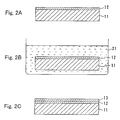
- Figures 2A to 2C are cross-sectional views showing another example of production processes in a method of the present invention.
- Figures 9A to 9C are cross-sectional views showing still another example of production processes in a method of the present invention.
- Figure 10 is a graph showing another example of current-voltage characteristics with respect to a pn junction produced by a method of the present invention and a pn junction produced by a method for producing a semiconductor device in a comparative example.
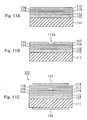
- Figures 11A to 11C are cross-sectional views showing still another example of production processes in a method of the present invention.
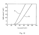
- Figure 12 is a graph showing still another example of current-light output characteristics with respect to a semiconductor laser produced by a method of the present invention and a semiconductor laser in a comparative example.
- Embodiment 1 an example of a method for producing a semiconductor device of the present invention will be described.
- Figures 2A to 2C show production processes in the method of Embodiment 1.
- a first semiconductor layer 12 made of a Group III nitride-based compound semiconductor is grown on a substrate 11.
- the first semiconductor layer 12 can be formed, for example, by metalorganic vapor phase epitaxy (MOVPE), hydride vapor phase epitaxy (HVPE), or molecular beam epitaxy (MBE).
- MOVPE metalorganic vapor phase epitaxy
- HVPE hydride vapor phase epitaxy
- MBE molecular beam epitaxy
- the first semiconductor layer 12 is formed in a reaction apparatus such as an MOVPE apparatus, an HVPE apparatus, or an MBE apparatus.
- a sapphire substrate or a substrate made of a Group III nitride-based compound semiconductor can be used as the substrate 11.
- the first semiconductor layer 12 is made of a Group III nitride-based compound semiconductor, i.e., a Group III-V compound semiconductor containing nitrogen as a Group V element.
- a Group III element at least one element selected from the group consisting of Ga, Al, and In can be used.
- the first semiconductor layer 12 may contain arsenic or phosphorus in addition to nitrogen, as the Group V element. More specifically, as a material for the first semiconductor layer 12, a semiconductor represented by Ga x In Y Al 1-X-Y N (0 ⁇ X ⁇ 1, 0 ⁇ Y ⁇ 1, X+Y ⁇ 1) can be used.
- the first semiconductor layer 12 may contain a dopant. Further, another semiconductor layer made of a Group III nitride-based compound semiconductor may be formed between the substrate 11 and the first semiconductor layer 12.
- the substrate 11 with the first semiconductor layer 12 formed thereon is taken out of the reaction apparatus and processed since an oxide layer and imparities adhere to the surface of the first semiconductor layer 12.
- the first semiconductor layer 12 is soaked in an alkaline aqueous solution 21 under the condition that a current is not flowing through the first semiconductor layer 12 (Process (a)). More specifically, the first semiconductor layer 12 is soaked in the solution under the condition that light having energy with a forbidden band width or larger of the first semiconductor layer 12 is not radiated to the first semiconductor layer 12.
- the alkaline aqueous solution include a potassium hydroxide aqueous solution, a sodium hydroxide aqueous solution, or an ammonia aqueous solution.
- a preferable pH value is varied depending upon the material of the first semiconductor layer 12 and the processing conditions.
- an alkaline aqueous solution for example, with a pH value of about 9 to 13 can be used.
- the temperature of the alkaline aqueous solution is in a range of 20°C to 130°C.
- the time for soaking the first semiconductor layer 12 in the alkaline aqueous solution is varied depending upon the pH thereof. It may be 1 to 10 minutes, for example. Because of Process (a), an oxide layer and impurities adhering to the surface of the first semiconductor layer 12 can be removed without etching the first semiconductor layer 12 excessively.
- the first semiconductor layer 12 is heated in gas containing nitrogen atoms (heating process).
- This heating process can be conducted by placing the first semiconductor layer 12 in the reaction apparatus, and introducing gas containing nitrogen atoms into the reaction apparatus while heating the substrate 11. More specifically, an MOVPE apparatus, an HVPE apparatus, or an MBE apparatus can be used.
- the heating temperature is in a range of 500°C to 1000°C, and more preferably at a temperature in a range of 600° to 900°C.
- the heating process may be omitted.
- Process (b) is conducted without exposing the second semiconductor layer 13 to the air after the heating process. More specifically, after conducting the heating process in the reaction apparatus, the process (b) should be conducted in the same apparatus.
- the second semiconductor layer 13 can be formed by a method similar to that of the first semiconductor layer 12.
- the second semiconductor layer 13 may be made of the same semiconductor as that of the first semiconductor layer 12, or may be made of a semiconductor different from that of the first semiconductor layer 12.
- the second semiconductor layer 13 may contain a dopant.
- the method for producing a semiconductor device in Embodiment 1 includes not only the above-mentioned production processes but also other production processes as described in examples, in accordance with a semiconductor device to be produced.
- an oxide layer and impurities adhering to the surface of the first semiconductor layer 12 are removed without etching it excessively. Therefore, the second semiconductor layer 13 with good crystallinity can be formed on the first semiconductor layer 12 exposed to the air.
- a heat treatment temperature in the heating process may be lower, so that the first semiconductor layer 12 is less influenced, and the second semiconductor layer 13 with particularly good crystallinity can be formed.
- Example 1 the case will be described with reference to Figures 9A to 9C in which a pn junction was formed by the method of Embodiment 1.
- an n-GaN layer (n-type GaN layer) 92 was grown on a sapphire substrate 91 in a reaction apparatus.
- the sapphire substrate 91 and the n-GaN layer 92 may be referred to as a substrate 93 collectively.
- the substrate 93 was placed in the MOVPE apparatus.
- the substrate 93 was heated to 1000°C, and a p-GaN layer (p-type GaN layer) 95 was grown on the n-GaN layer 92 by an MOVPE method, as shown in Figure 9C, whereby a pn junction 96 was formed.
- an oxide layer and impurities adhering to the surface of the n-GaN layer 92 were removed by using a potassium hydroxide aqueous solution. Therefore, an oxide layer and impurities can be removed efficiently while the surface of the n-GaN layer 92 was prevented from being roughened.
- an oxide layer is dissolved easily in a potassium hydroxide aqueous solution, so that the oxide layer on the surface of the n-GaN layer 92 can be removed efficiently.
- the p-GaN layer 95 is grown on the n-GaN layer 92 from which an oxide layer and impurities have been removed, the p-GaN layer 95 with good crystallinity can be formed.
- a pn junction in the comparative example was produced.
- the n-GaN layer 92 was subjected to surface treatment using phosphoric acid, which has been conducted conventionally. Thereafter, a p-GaN layer was formed to produce a pn junction.
- the pn junction 96 and the pn junction in the comparative example also were evaluated for characteristics.
- the surface of the p-GaN layer 95 was observed by photography with an optical microscope at a 1000-fold magnification. Consequently, the p-GaN layer 95 was found to have a mirror surface with little unevenness. It is considered that this is because the n-GaN layer 92 had a mirror surface with little unevenness, and the p-GaN layer 95 formed thereon also had a mirror surface.
- the concentrations of carbon and oxygen atoms at the interface of the pn junction 96 were 2 ⁇ 10 18 /cm 3 and 2 ⁇ 10 17 /cm 3 , respectively.
- the concentrations of carbon and oxygen atoms at the interface of the pn junction in the comparative example were 1 ⁇ 10 19 /cm 3 and 6 ⁇ 10 18 /cm 3 , respectively. From this, it was found that an oxide layer and impurities adhering to the surface of the n-GaN layer 92 were removed effectively by the surface treatment in Example 4, and the surface of the n-GaN layer 92 was cleaned effectively.
- Figure 10 shows current-voltage characteristics (line a) of the pn junction 96 and current voltage characteristics (line b) in the comparative example.
- a rise voltage of the pn junction 96 was 3.4 volts
- a rise voltage of the pn junction in the comparative example was 4.1 volts. From this, it can be understood that a satisfactory pn junction, which was not realized by the conventional surface treatment, was formed by the method of Example 4. The reason for this is considered that the surface of the n-GaN layer 92 was cleaned effectively.
- the specific resistance of the p-GaN layer was measured to be 0.3 ⁇ cm in the case of the pn junction in the comparative example, whereas the specific resistance of the p-GaN layer was measured to be 0.1 ⁇ cm in the case of the pn junction 96. From this, it was found that the p-GaN layer 92 with good crystallinity was formed by the surface treatment in Example 1.
- Example 1 According to the method of Example 1, the same effects can be obtained even when a sodium hydroxide aqueous solution or an ammonia aqueous solution is used in place of potassium hydroxide aqueous solution.
- Example 2 the case will be described with reference to Figures 11A to 11C in which a semiconductor laser with a current confinement layer was produced by the method of Embodiment 1.
- a substrate 111 made of n-type GaN was prepared.
- the substrate 111 was produced by growing an n-GaN layer on a sapphire substrate, and removing the sapphire substrate by polishing. Then, the surface of the substrate 111 was cleaned under the same conditions as those in Example 1. More specifically, the substrate 111 was subjected to heat treatment in an atmosphere of mixed gas (ammonia and hydrogen gas) in an MOVPE apparatus.
- mixed gas ammonia and hydrogen gas
- “slm” denotes a unit of a flow rate
- “1 slm” means that 1 L of gas in a standard state is allowed to flow for one minute.
- a cladding layer 112 (thickness: 1 ⁇ m) made of n-type AlGaN, a light guide layer 113 (thickness: 0.3 ⁇ m) made of n-type GaN, an active layer 114 made of InGaN, a light guide layer 115 (thickness: 0.05 ⁇ m) made of p-type GaN, a first p-AlGaN cladding layer 116 (thickness: 0.05 ⁇ m) made of p-type AlGaN, and a current confinement layer 117 (thickness: 0.5 ⁇ m) made of n-type AlGaN were formed on the substrate 111 successively by an MOVPE method.
- the atomic ratio between Al and Ga in the cladding layer 112 was set at 10 : 90.
- the active layer 114 had a multi-quantum well structure. More specifically, the active layer 114 is composed of a barrier layer (thickness: 3 nm, not shown) made of InGaN, and a well layer (thickness: 6 nm, not shown) made of InGaN.
- the atomic ratio between In and Ga in the barrier layer was set at 3 : 97, and the atomic ratio between In and Ga in the well layer was set at 15 : 85.
- the substrate 111 was taken out of the MOVPE apparatus, and an opening 117h in a stripe shape (width: 2 ⁇ m) was formed in the current confinement layer 117 by etching, as shown in Figure 11B.
- “slm” denotes a unit of a flow rate
- “1 slm” means that 1 L of gas in a standard state is allowed to flow for one minute.
- a second p-AlGaN cladding layer 118 (thickness: 1 ⁇ m) made of p-type AlGaN and a contact layer 119 (thickness: 0.1 ⁇ m) made of p-type GaN were formed successively on the first p-AlGaN cladding layer 116 and the current confinement layer 117 by an MOVPE method.
- the atomic ratio between Al and Ga in the p-AlGaN cladding layer 118 was set at 10 : 90.
- an n-side electrode 120 was formed on the back surface of the substrate 111, and a p-side electrode 121 was formed on the contact layer 119, whereby a semiconductor laser (semiconductor device) 122 was produced.
- a semiconductor laser was produced under the same conditions as those in the semiconductor laser 122 except that the substrate 111 and the current confinement layer 117 were subjected to surface treatment by using phosphoric acid, which has been used conventionally.
- this semiconductor laser will be referred to as a semiconductor laser in the comparative example.
- the substrate 111 and the current confinement layer 117 were subjected to heat treatment in an atmosphere of mixed gas (ammonia and hydrogen gas) after the surface treatment by potassium hydroxide aqueous solution. Therefore, water molecules, which adhere to the substrate 111 and the current confinement layer 117 when they are soaked in the potassium hydroxide aqueous solution, can be removed, and the surfaces of the substrate 111 and the current confinement layer 117 can be cleaned particularly. Consequently, the crystallinity of a Group III nitride-based compound semiconductor grown on the substrate 111 can be rendered particularly satisfactory.
- mixed gas ammonia and hydrogen gas
- Figure 12 shows current-light output characteristics (line a) of the semiconductor laser 122 and current-light output characteristics (line b) of the semiconductor laser in the comparative example. It is understood from Figure 12 that a threshold current and a working current of the semiconductor laser 122 are smaller than those of the semiconductor laser in the comparative example. It is considered that this is because the surface of the first p-AlGaN cladding layer 116 was cleaned sufficiently, so that the second p-AlGaN cladding layer 118 with good crystallinity was formed; as a result, an electrical resistance and a light loss at the interface between the first p-AlGaN cladding layer 116 and the second p-AlGaN cladding layer 117 were reduced.
- a durability test was conducted with respect to the semiconductor laser 122 and the semiconductor laser in the comparative example.
- the durability test was conducted by operating a plurality of semiconductor lasers at a temperature of 25°C and a constant light output (30 mW). About half of the semiconductor lasers in the comparative example were disabled after 1000 hours from the commencement of the durability test. The remaining semiconductor lasers also were degraded considerably in device characteristics (i.e., a working current increased by 60% on average). On the other hand, all the semiconductor lasers 122 were operational even after 1000 hours from the commencement of the durability test, and a working current increased by 2% on average. Thus, the reliability of the semiconductor laser in Example 1 was enhanced remarkably.
- the surface of a first semiconductor layer made of nitride-based compound semiconductor can be cleaned while the flatness of the surface is maintained. Therefore, according to the method of the present invention, a second semiconductor layer made of a nitride-based compound semiconductor with good crystallinity can be grown on the first semiconductor layer. Consequently, a semiconductor device with good characteristics and high reliability can be produced.
- the method for producing a semiconductor device of the present invention is applicable to a semiconductor device in which at least two Group III nitride-based compound semiconductors are layered.
- the method is applicable to a semiconductor laser, a light-emitting diode, an FET, and the like.
Landscapes
- Chemical & Material Sciences (AREA)
- Nanotechnology (AREA)
- Engineering & Computer Science (AREA)
- Crystallography & Structural Chemistry (AREA)
- Optics & Photonics (AREA)
- Biophysics (AREA)
- Physics & Mathematics (AREA)
- Life Sciences & Earth Sciences (AREA)
- Semiconductor Lasers (AREA)
- Led Devices (AREA)
- Weting (AREA)
- Drying Of Semiconductors (AREA)
- Junction Field-Effect Transistors (AREA)
Applications Claiming Priority (3)
| Application Number | Priority Date | Filing Date | Title |
|---|---|---|---|
| JP36987199 | 1999-12-27 | ||
| JP2000027453 | 2000-02-04 | ||
| EP00128255A EP1113485A3 (fr) | 1999-12-27 | 2000-12-22 | Procédé de fabrication d'un dispositif semiconducteur |
Related Parent Applications (1)
| Application Number | Title | Priority Date | Filing Date |
|---|---|---|---|
| EP00128255A Division EP1113485A3 (fr) | 1999-12-27 | 2000-12-22 | Procédé de fabrication d'un dispositif semiconducteur |
Publications (1)
| Publication Number | Publication Date |
|---|---|
| EP1727189A2 true EP1727189A2 (fr) | 2006-11-29 |
Family
ID=26582166
Family Applications (2)
| Application Number | Title | Priority Date | Filing Date |
|---|---|---|---|
| EP06018320A Withdrawn EP1727189A2 (fr) | 1999-12-27 | 2000-12-22 | Procédé de fabrication d'un dispositif semiconducteur |
| EP00128255A Withdrawn EP1113485A3 (fr) | 1999-12-27 | 2000-12-22 | Procédé de fabrication d'un dispositif semiconducteur |
Family Applications After (1)
| Application Number | Title | Priority Date | Filing Date |
|---|---|---|---|
| EP00128255A Withdrawn EP1113485A3 (fr) | 1999-12-27 | 2000-12-22 | Procédé de fabrication d'un dispositif semiconducteur |
Country Status (4)
| Country | Link |
|---|---|
| US (1) | US6673702B2 (fr) |
| EP (2) | EP1727189A2 (fr) |
| JP (1) | JP2001291703A (fr) |
| KR (1) | KR100440705B1 (fr) |
Families Citing this family (13)
| Publication number | Priority date | Publication date | Assignee | Title |
|---|---|---|---|---|
| JP4037154B2 (ja) * | 2002-04-15 | 2008-01-23 | 松下電器産業株式会社 | プラズマ処理方法 |
| US9279193B2 (en) | 2002-12-27 | 2016-03-08 | Momentive Performance Materials Inc. | Method of making a gallium nitride crystalline composition having a low dislocation density |
| KR100576850B1 (ko) * | 2003-10-28 | 2006-05-10 | 삼성전기주식회사 | 질화물 반도체 발광소자 제조방법 |
| CN1638055A (zh) * | 2003-12-24 | 2005-07-13 | 松下电器产业株式会社 | 氮化物系化合物半导体元件的制造方法 |
| US7626217B2 (en) * | 2005-04-11 | 2009-12-01 | Cree, Inc. | Composite substrates of conductive and insulating or semi-insulating group III-nitrides for group III-nitride devices |
| US7446345B2 (en) * | 2005-04-29 | 2008-11-04 | Cree, Inc. | Light emitting devices with active layers that extend into opened pits |
| US20110018105A1 (en) * | 2005-05-17 | 2011-01-27 | Sumitomo Electric Industries, Ltd. | Nitride-based compound semiconductor device, compound semiconductor device, and method of producing the devices |
| JP2006352075A (ja) * | 2005-05-17 | 2006-12-28 | Sumitomo Electric Ind Ltd | 窒化物系化合物半導体および化合物半導体の洗浄方法、これらの製造方法および基板 |
| US9331192B2 (en) * | 2005-06-29 | 2016-05-03 | Cree, Inc. | Low dislocation density group III nitride layers on silicon carbide substrates and methods of making the same |
| JP4967914B2 (ja) * | 2006-08-22 | 2012-07-04 | 豊田合成株式会社 | 発光素子の製造方法 |
| DE102007019079A1 (de) * | 2007-01-26 | 2008-07-31 | Osram Opto Semiconductors Gmbh | Verfahren zum Herstellen eines optoelektronischen Halbleiterchips und optoelektronischer Halbleiterchip |
| JP5003527B2 (ja) * | 2008-02-22 | 2012-08-15 | 住友電気工業株式会社 | Iii族窒化物発光素子、及びiii族窒化物系半導体発光素子を作製する方法 |
| JP4787891B2 (ja) * | 2009-06-09 | 2011-10-05 | 住友電気工業株式会社 | エピタキシャル層形成用iii族窒化物結晶基板、エピタキシャル層付iii族窒化物結晶基板および半導体デバイス |
Family Cites Families (13)
| Publication number | Priority date | Publication date | Assignee | Title |
|---|---|---|---|---|
| US4335506A (en) * | 1980-08-04 | 1982-06-22 | International Business Machines Corporation | Method of forming aluminum/copper alloy conductors |
| US5631190A (en) * | 1994-10-07 | 1997-05-20 | Cree Research, Inc. | Method for producing high efficiency light-emitting diodes and resulting diode structures |
| JP3575859B2 (ja) | 1995-03-10 | 2004-10-13 | 株式会社東芝 | 半導体基板の表面処理方法及び表面処理装置 |
| JPH0945670A (ja) * | 1995-07-29 | 1997-02-14 | Hewlett Packard Co <Hp> | Iii族−n系結晶の気相エッチング方法および再成長方法 |
| WO1997008356A2 (fr) | 1995-08-18 | 1997-03-06 | The Regents Of The University Of California | Depot en phase gazeuse par procede chimique organometallique modifie de couches minces des groupes iii a v |
| JPH09232681A (ja) | 1996-02-22 | 1997-09-05 | Hitachi Ltd | 窒化物系化合物半導体光素子 |
| JP3344287B2 (ja) | 1996-08-30 | 2002-11-11 | 住友電気工業株式会社 | Ii−vi族化合物半導体結晶の表面清浄化方法 |
| TW349132B (en) | 1996-08-30 | 1999-01-01 | Sumitomo Electric Industries | Surface cleaning method of II-VI Group compound semiconductor crystal |
| JPH10163114A (ja) * | 1996-11-29 | 1998-06-19 | Matsushita Electron Corp | 半導体装置およびその製造方法 |
| TW385493B (en) * | 1997-08-04 | 2000-03-21 | Sumitomo Chemical Co | Method for manufacturing group III-V compound semiconductor |
| JP3794876B2 (ja) * | 1998-09-09 | 2006-07-12 | 松下電器産業株式会社 | 半導体装置の製造方法 |
| JP2000183465A (ja) * | 1998-12-18 | 2000-06-30 | Pioneer Electronic Corp | 3族窒化物半導体素子製造方法 |
| GB2350927A (en) * | 1999-06-12 | 2000-12-13 | Sharp Kk | A method growing nitride semiconductor layer by molecular beam epitaxy |
-
2000
- 2000-12-22 EP EP06018320A patent/EP1727189A2/fr not_active Withdrawn
- 2000-12-22 EP EP00128255A patent/EP1113485A3/fr not_active Withdrawn
- 2000-12-26 JP JP2000395312A patent/JP2001291703A/ja active Pending
- 2000-12-26 US US09/748,436 patent/US6673702B2/en not_active Expired - Fee Related
- 2000-12-27 KR KR10-2000-0082697A patent/KR100440705B1/ko not_active Expired - Fee Related
Also Published As
| Publication number | Publication date |
|---|---|
| KR100440705B1 (ko) | 2004-07-15 |
| US20010021572A1 (en) | 2001-09-13 |
| EP1113485A3 (fr) | 2005-08-31 |
| EP1113485A2 (fr) | 2001-07-04 |
| US6673702B2 (en) | 2004-01-06 |
| KR20010078747A (ko) | 2001-08-21 |
| JP2001291703A (ja) | 2001-10-19 |
Similar Documents
| Publication | Publication Date | Title |
|---|---|---|
| JP3688843B2 (ja) | 窒化物系半導体素子の製造方法 | |
| JP3470623B2 (ja) | 窒化物系iii−v族化合物半導体の成長方法、半導体装置の製造方法および半導体装置 | |
| US6829273B2 (en) | Nitride semiconductor layer structure and a nitride semiconductor laser incorporating a portion of same | |
| JP3433075B2 (ja) | 窒化物系半導体素子の製造方法 | |
| US20010038656A1 (en) | Nitride semiconductor device | |
| US20050218414A1 (en) | 4H-polytype gallium nitride-based semiconductor device on a 4H-polytype substrate | |
| EP1196971B1 (fr) | Structure en couches de semiconducteur au nitrure et laser a semiconducteur au nitrure en contenant une partie | |
| WO2008054994A2 (fr) | Dispositif luminescent en uv profond et procédé de fabrication | |
| EP1727189A2 (fr) | Procédé de fabrication d'un dispositif semiconducteur | |
| JPH11251687A (ja) | 半導体の製造方法及び半導体装置 | |
| US6960482B2 (en) | Method of fabricating nitride semiconductor and method of fabricating semiconductor device | |
| JP2000082863A (ja) | 半導体発光素子の製造方法 | |
| US20030222266A1 (en) | Gallium-nitride-based compound semiconductor device | |
| JP2999435B2 (ja) | 半導体の製造方法及び半導体発光素子 | |
| WO2000024097A1 (fr) | Laser ameliore a semi-conducteur au nitrure a champ lointain | |
| JPH08203862A (ja) | 窒化物系化合物半導体のエッチング方法 | |
| JP2002151415A (ja) | 窒化物系半導体素子、窒化物系半導体基板、及びそれらの製造方法 | |
| JP4419520B2 (ja) | 半導体レーザダイオード及びその製造方法 | |
| US20070196938A1 (en) | Nitride semiconductor device and method for fabricating the same | |
| JP3927646B2 (ja) | 窒化ガリウム系化合物半導体発光素子及びその製造方法 | |
| JP2003179027A (ja) | 窒化物系化合物半導体のエッチング方法 | |
| JPH08264830A (ja) | 発光素子の製造方法 | |
| JPH11274555A (ja) | 半導体素子 | |
| JPH0983079A (ja) | 半導体素子 | |
| US20040105475A1 (en) | Semiconductor laser device including cladding layer having stripe portion different in conductivity type from adjacent portions |
Legal Events
| Date | Code | Title | Description |
|---|---|---|---|
| PUAI | Public reference made under article 153(3) epc to a published international application that has entered the european phase |
Free format text: ORIGINAL CODE: 0009012 |
|
| 17P | Request for examination filed |
Effective date: 20060901 |
|
| AC | Divisional application: reference to earlier application |
Ref document number: 1113485 Country of ref document: EP Kind code of ref document: P |
|
| AK | Designated contracting states |
Kind code of ref document: A2 Designated state(s): DE FR GB |
|
| RAP1 | Party data changed (applicant data changed or rights of an application transferred) |
Owner name: PANASONIC CORPORATION |
|
| STAA | Information on the status of an ep patent application or granted ep patent |
Free format text: STATUS: THE APPLICATION HAS BEEN WITHDRAWN |
|
| 18W | Application withdrawn |
Effective date: 20090219 |