EP1729342A1 - Kühlkörperplatte und herstellungsverfahren dafür - Google Patents
Kühlkörperplatte und herstellungsverfahren dafür Download PDFInfo
- Publication number
- EP1729342A1 EP1729342A1 EP05721048A EP05721048A EP1729342A1 EP 1729342 A1 EP1729342 A1 EP 1729342A1 EP 05721048 A EP05721048 A EP 05721048A EP 05721048 A EP05721048 A EP 05721048A EP 1729342 A1 EP1729342 A1 EP 1729342A1
- Authority
- EP
- European Patent Office
- Prior art keywords
- heat sink
- heat
- bonding
- board
- fitted
- Prior art date
- Legal status (The legal status is an assumption and is not a legal conclusion. Google has not performed a legal analysis and makes no representation as to the accuracy of the status listed.)
- Withdrawn
Links
Images


Classifications
-
- H—ELECTRICITY
- H10—SEMICONDUCTOR DEVICES; ELECTRIC SOLID-STATE DEVICES NOT OTHERWISE PROVIDED FOR
- H10W—GENERIC PACKAGES, INTERCONNECTIONS, CONNECTORS OR OTHER CONSTRUCTIONAL DETAILS OF DEVICES COVERED BY CLASS H10
- H10W40/00—Arrangements for thermal protection or thermal control
- H10W40/10—Arrangements for heating
-
- H—ELECTRICITY
- H10—SEMICONDUCTOR DEVICES; ELECTRIC SOLID-STATE DEVICES NOT OTHERWISE PROVIDED FOR
- H10W—GENERIC PACKAGES, INTERCONNECTIONS, CONNECTORS OR OTHER CONSTRUCTIONAL DETAILS OF DEVICES COVERED BY CLASS H10
- H10W90/00—Package configurations
- H10W90/701—Package configurations characterised by the relative positions of pads or connectors relative to package parts
- H10W90/731—Package configurations characterised by the relative positions of pads or connectors relative to package parts of die-attach connectors
- H10W90/734—Package configurations characterised by the relative positions of pads or connectors relative to package parts of die-attach connectors between a chip and a stacked insulating package substrate, interposer or RDL
Definitions
- the present invention relates to a heat sink board and a manufacturing method thereof. More particularly, the present invention relates to a heat sink board suitable for mounting an electronic component generating heat in large amount, in particular a semiconductor component, such as an inverter or a power module used in an electric vehicle, and also relates to a manufacturing method of the heat sink board.
- a semiconductor component such as an inverter or a power module used in an electric vehicle
- a heat sink board for mounting an electronic component generating heat in large amount, in particular a semiconductor component has been basically made of a copper (Cu) material and generally formed of a one-piece plate. That type of heat sink board is inexpensive because of using a one-piece plate and has good heat radiation because of using copper as the material.
- Cu copper
- the copper (Cu) material has a large linear expansion coefficient of 16.6 (ppm/°C) and faces a problem that heat generated from the mounted semiconductor component causes a crack due to thermal stress generated in a surface bonded using a solder, which has a different linear expansion coefficient.
- a heat sink board in the form of a one-piece plate using, instead of the copper material, a copper-molybdenum (Cu-Mo) composite material that has a small linear expansion coefficient of 9.2 (ppm/°C) and relatively good heat radiation.
- the heat sink board is very expensive because the one-piece board is made of the Cu-Mo composite material containing a large amount of molybdenum (Mo) that has a high material cost.
- Patent Document 1 JP,A 8-186204 discloses a heat sink board comprising a mount portion made of a material having a thermal expansion coefficient close to that of a semiconductor device, and a heat radiating member made of a material having superior thermal conduction and dissipation characteristics, the mount portion and the heat radiating member being brought into an integral structure by infiltration bonding under heating.
- Patent Document 2 JP,A 6-77678 discloses a heat sink board in which a hole is formed in a predetermined position of a base material made of a nickel-iron alloy, and a heat radiating member made of a copper-based metal is embedded in the hole by screwing or pressing, thereby forming an integral board.
- the heat sink board made of plural members must be held in close adhesion to a heat generating source in order to radiate heat with high efficiency.
- the heat generating source is a semiconductor
- the semiconductor is mounted to the board by soldering, and hence the heat sink board is required to have satisfactory product accuracy, such as high flatness.
- Patent Document 1 has the problem that, because of using the bonding method performed under application of heat, such as welding or brazing, the bonding accuracy is reduced due to a thermal deformation, etc., and mechanical machining is required on a soldered surface or other relevant surface after the bonding.
- the application of heat also makes Patent Document 1 disadvantageous in points of energy loss and material yield.
- Patent Document 2 using the screwing method, the degree of close adhesion between the base material and the heat radiating member in the fastened portion is low and a sufficient effective screw length cannot be obtained in a thin plate like the heat sink board. Also, the screwing method accompanies with a risk of loosening. Further, the pressing method is disadvantageous in points of productivity and cost. In other words, because the pressing imposes deformation pressure on the heat radiating member made of a relatively soft material, desired flatness is hard to obtain and a flat-surface finishing step is required in some cases.
- An object of the invention is to provide a heat sink board and a manufacturing method thereof, which can realize a high product accuracy and superior productivity.
- the present invention provides a heat sink board formed by bonding, to a first heat sink, a second heat sink having a smaller linear expansion coefficient than that of the first heat sink, wherein the second heat sink is fitted to the first heat sink, and a material of the first heat sink in the vicinity of a boundary between the fitted heat sinks is plastically deformed for close adhesion to the second heat sink.
- the second heat sink is a chip member for mounting a semiconductor component.
- the first heat sink has a plastic-bonding pressed groove, which is formed in a bonded surface thereof at the boundary between the fitted heat sinks and which receives the second heat sink.
- the first heat sink is made of a Cu-based material
- the second heat sink is made of a Cu-Mo composite material.
- an entire peripheral edge of the second heat sink is exposed with formation of a pressing mark recessed by the plastic flow bonding.
- the semiconductor component is fixed to the second heat sink by soldering.
- the first heat sink and the second heat sink are bonded to each other by the plastic flow bonding with a thermally conductive paste or wax interposed between an inner peripheral surface of the first heat sink and an outer peripheral surface of the second heat sink.
- the first heat sink and the second heat sink are bonded to each other by the plastic flow bonding with a thermally conductive paste or wax interposed between a bottom surface of the first heat sink and a lower surface of the second heat sink.
- the present invention also provides a method of manufacturing a heat sink board formed by bonding, to a first heat sink, a second heat sink having a smaller linear expansion coefficient than that of the first heat sink, the method comprising the steps of:
- the second heat sink is fitted to the fitting hole of the first heat sink, and the material of the first heat sink at the boundary between the fitted heat sinks is plastically deformed for bonding to the second heat sink.
- the bonding between the first and second heat sinks can be preformed at room temperature, and the heat sink board made of a composite member and having a high flat-surface accuracy can be easily and reliably obtained.
- the heat sink board is manufactured by fitting the second heat sink to the first heat sink and locally plastically deforming the material in the peripheral portion of the first heat sink in contact with the second heat sink by the bonding punch which is descended along the outer peripheral wall of the second heat sink, thereby integrating the two heat sinks with each other by plastic flow bonding
- the plastic-bonding pressed groove (pressing mark) formed in the first heat sink by the pressing near the second heat sink (chip) serves to prevent a solder from overflowing with no need of a special jig when the semiconductor is mounted, and the heat sink for mounting a heat generating component can be manufactured with high productivity.
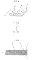
- Fig. 1 is a perspective view showing an example of a heat sink structure according to the present invention
- Fig. 2 is an enlarged vertical sectional view of an essential part in Fig. 1
- Fig. 3 is a vertical sectional view of a power module including a semiconductor mounted to a heat sink.
- a heat sink board 1 shown in Figs. 1 and 2 comprises a first heat sink 2 in the form of a plate made of a copper (Cu) material, and a second heat sink 3 made of a material having a smaller linear expansion coefficient than that of Cu, such as a Cu-Mo composite material.
- Cu copper
- a plurality of through holes 3 are formed in the first heat sink 2 corresponding to the number of components to be mounted.
- the second heat sink 3 formed as a disk-like chip member is fitted into each of the holes 3 and is integrally bonded to the first heat sink 2 by plastic deformation.
- the second heat sink 3 is fitted to the first heat sink 2 such that an electronic-component mounted surface 5 of the second heat sink 3 is flush with the surface of the first heat sink 2.
- An entire peripheral portion of the first heat sink 3 in the vicinity of a boundary between the fitted heat sinks is pressed so as to bring the two heat sinks into an integral structure by plastic flow bonding.
- Fig. 3 shows a state where a semiconductor component is mounted to the second heat sink of the heat sink board 1.
- a semiconductor is mounted to the heat sink board 1 as shown in Fig. 3, and heat generated from the semiconductor is radiated primarily through the heat sink board 1.
- a Cu plate 10 is bonded to one surface 5 of the second heat sink 4 by using a solder 11, and a silicon nitride plate 13 is bonded to the Cu plate 10 by using an Ag solder 12. Further, a Cu plate 15 is bonded to the silicon nitride plate 13 by using an Ag solder 14, and a semiconductor chip 17 is bonded to the Cu plate 15 by using a solder 16.
- aluminum wires, etc. are bonded to the semiconductor chip 17 for electric wiring, thereby constituting a semiconductor device.
- the solder 11 can be avoided from causing a crack due to the difference in linear expansion coefficient between different materials at high temperature, and the expensive Cu-Mo composite material is used in small amount. As a result, it is possible to realize resource saving and to obtain a very rational device.
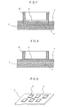
- the plate-like first heat sink 2 made of Cu and having the plurality of through holes 4 formed therein, shown in Fig. 4, and the disk-like second heat sink 3 made of the Cu-Mo composite material, shown in Fig. 5, are placed and set on a lower die 7 in such a state that the second heat sink 3 is fitted into each of the fitting holes 4 of the first heat sink 2 as shown in Fig. 6. Because Cu is so soft as to be plastically deformed with ease and Cu-Mo is harder than Cu, the combination of those materials is suitable for the plastic flow bonding. Even when the fitting hole 4 of the first heat sink 2 is formed by punching and is in a stated hardened as a result of the punching, the difference in hardness between the two materials can be ensured and no problems are caused from the practical point of view.
- the plastic flow of the material of the first heat sink 3 can be developed toward a lateral surface of the second heat sink 3 just by a small punch force when the first heat sink 3 is bonded to the first heat sink 2, parallelism of the heat sink board is not affected and the heat sink board having a very high product accuracy can be obtained.
- the second heat sink 3 is preferably in the form of a disk, it may be rectangular as shown in Fig. 9, or elliptic.
- the hole 6 of the first heat sink 2 may be a bottom-equipped hole instead of a through hole.
- a second heat sink 31 is placed in a through hole of a first heat sink 21 with a thermally conductive paste or wax 20 (generally a silicone paste) interposed between them, and the two heat sinks are brought into an integral structure by the plastic flow bonding.
- a thermally conductive paste or wax 20 generally a silicone paste
- the plastic flow bonding of metals is performed, as seen from Figs. 7 and 8, such that a portion of one of bonded members positioned around the other member is locally pressed by a punch, thus causing a material of the concentrically pressed member to just flow in the vertical direction. Therefore, the material in a portion far away from the fore end of the punch is hardly plastically deformed.
- the performance of a heat radiating member formed by bonding two members to each other depends on the degree of close adhesion between the bonded two members.
- an annular groove is formed in a substantially central area of the first heat sink 21 or the second heat sink 31 which is not subjected to the plastic deformation pressure, and a thermally conductive paste or wax 20 is applied to the annular groove, followed by punching the first heat sink from both sides.
- annular pressing marks (recesses) 61 and 62 are formed by the punching on both sides of the first heat sink.
- the punching position can be optionally selected, as shown, depending on the plate thickness, the applied position of the thermally conductive paste or wax 20, etc.
- the method employed in Embodiment 4 to overcome the problem of thermal conduction is applied to a first heat sink 22 having a bottom-equipped hole.
- a thermally conductive paste or wax 23 is previously applied to a bottom surface of the bottom-equipped hole or a bottom surface of the second heat sink 3.
- a second heat sink 3 having a diameter slightly smaller than or equal to that of the bottom-equipped hole is placed in the bottom-equipped hole.
- the boundary between the two heat sinks is pressed by a punch such that a material of the member just below the punch is plastically deformed in the vertical direction and toward a material of the second heat sink 32 for bonding between the two heat sinks.
- the thermally conductive paste 23 is compressed to increase the degree of close adhesion.
- any of the above-described embodiments employs the method of forming the heat sink board 1 by integrating the second heat sink 3 with the first heat sink 2 through the plastic flow bonding, and then mounting the electronic component to the heat sink board 1 in the bonded state.
- the method may be modified such that the electronic component is first mounted to the second heat sink 3, and the second heat sink 3 is then integrated with the first heat sink 2 by the plastic flow bonding.
- a heat sink board can be provided which is suitable for mounting an electronic component generating heat in large amount, in particular a semiconductor component, such as an inverter or a power module used in an electric vehicle, and which has a variety of application fields.
Landscapes
- Cooling Or The Like Of Semiconductors Or Solid State Devices (AREA)
Applications Claiming Priority (2)
| Application Number | Priority Date | Filing Date | Title |
|---|---|---|---|
| JP2004077371 | 2004-03-18 | ||
| PCT/JP2005/004861 WO2005091363A1 (ja) | 2004-03-18 | 2005-03-11 | ヒートシンク基板とその製造方法 |
Publications (2)
| Publication Number | Publication Date |
|---|---|
| EP1729342A1 true EP1729342A1 (de) | 2006-12-06 |
| EP1729342A4 EP1729342A4 (de) | 2009-11-11 |
Family
ID=34993973
Family Applications (1)
| Application Number | Title | Priority Date | Filing Date |
|---|---|---|---|
| EP05721048A Withdrawn EP1729342A4 (de) | 2004-03-18 | 2005-03-11 | Kühlkörperplatte und herstellungsverfahren dafür |
Country Status (3)
| Country | Link |
|---|---|
| EP (1) | EP1729342A4 (de) |
| JP (1) | JP4415988B2 (de) |
| WO (1) | WO2005091363A1 (de) |
Cited By (2)
| Publication number | Priority date | Publication date | Assignee | Title |
|---|---|---|---|---|
| WO2009078767A1 (en) * | 2007-12-17 | 2009-06-25 | Telefonaktiebolaget Lm Ericsson (Publ) | A device for reducing thermal stress on connection points |
| WO2013030001A1 (de) * | 2011-08-26 | 2013-03-07 | Robert Bosch Gmbh | Halbleiterbauelement mit einem kühlkörper |
Families Citing this family (2)
| Publication number | Priority date | Publication date | Assignee | Title |
|---|---|---|---|---|
| DE102006045939B4 (de) * | 2006-09-28 | 2021-06-02 | Infineon Technologies Ag | Leistungshalbleitermodul mit verbesserter Temperaturwechselstabilität |
| CN104093293B (zh) * | 2014-04-01 | 2017-10-27 | 东莞汉旭五金塑胶科技有限公司 | 金属散热板与热导管的嵌合组成及其制法 |
Family Cites Families (6)
| Publication number | Priority date | Publication date | Assignee | Title |
|---|---|---|---|---|
| JPH08186204A (ja) * | 1994-11-02 | 1996-07-16 | Nippon Tungsten Co Ltd | ヒートシンク及びその製造方法 |
| JPH09225562A (ja) * | 1996-02-17 | 1997-09-02 | Arai:Kk | 金属片へのピン取付構造及び方法 |
| JP3220105B2 (ja) * | 1998-02-25 | 2001-10-22 | 株式会社鈴木 | 半導体装置用ヒートスプレッダと半導体装置用パッケージ |
| JP2000077582A (ja) * | 1998-08-31 | 2000-03-14 | Kawai Musical Instr Mfg Co Ltd | 放熱材 |
| JP2000151163A (ja) * | 1998-11-18 | 2000-05-30 | Showa Alum Corp | ヒートシンクの製造法 |
| JP3611548B2 (ja) * | 2002-02-20 | 2005-01-19 | Tdk株式会社 | スイッチング電源とその製造方法 |
-
2005
- 2005-03-11 EP EP05721048A patent/EP1729342A4/de not_active Withdrawn
- 2005-03-11 JP JP2006511230A patent/JP4415988B2/ja not_active Expired - Fee Related
- 2005-03-11 WO PCT/JP2005/004861 patent/WO2005091363A1/ja not_active Ceased
Cited By (4)
| Publication number | Priority date | Publication date | Assignee | Title |
|---|---|---|---|---|
| WO2009078767A1 (en) * | 2007-12-17 | 2009-06-25 | Telefonaktiebolaget Lm Ericsson (Publ) | A device for reducing thermal stress on connection points |
| US20100271780A1 (en) * | 2007-12-17 | 2010-10-28 | Schoeoen Martin | Device for reducing thermal stress on connection points |
| US8233281B2 (en) | 2007-12-17 | 2012-07-31 | Telefonaktiebolaget L M Ericsson (Publ) | Device for reducing thermal stress on connection points |
| WO2013030001A1 (de) * | 2011-08-26 | 2013-03-07 | Robert Bosch Gmbh | Halbleiterbauelement mit einem kühlkörper |
Also Published As
| Publication number | Publication date |
|---|---|
| WO2005091363A1 (ja) | 2005-09-29 |
| EP1729342A4 (de) | 2009-11-11 |
| JPWO2005091363A1 (ja) | 2008-02-07 |
| JP4415988B2 (ja) | 2010-02-17 |
Similar Documents
| Publication | Publication Date | Title |
|---|---|---|
| KR101539250B1 (ko) | 열적으로 강화된 박형 반도체 패키지 | |
| CN103227154B (zh) | 具有压印底板的功率半导体模块及其制造方法 | |
| US6504238B2 (en) | Leadframe with elevated small mount pads | |
| KR20060004996A (ko) | 통합된 열 분산기 리드 | |
| JP2009054731A (ja) | 放熱部付き金属ベースプリント基板及びその製造方法 | |
| CN111584474B (zh) | 半导体装置的制造方法 | |
| JPH05243457A (ja) | 半導体素子構造および金属プレートの作製方法および電流伝達端子の作製方法 | |
| US20050180111A1 (en) | Low thermal stress composite heat sink assembly | |
| EP3425666A1 (de) | Halbleitermodul | |
| US7468554B2 (en) | Heat sink board and manufacturing method thereof | |
| CN114342069B (zh) | 功率半导体装置及其制造方法 | |
| JP3669980B2 (ja) | モジュール構造体の製造方法並びに回路基板の固定方法及び回路基板 | |
| EP1729342A1 (de) | Kühlkörperplatte und herstellungsverfahren dafür | |
| JP2004336046A (ja) | 特定用途向けヒートシンク素子 | |
| JP6048893B2 (ja) | 樹脂パッケージ | |
| JPH09181253A (ja) | 半導体素子用のパッケージング装置 | |
| JP5098239B2 (ja) | モールドパッケージおよびその製造方法 | |
| JP2003258167A (ja) | 構造物 | |
| WO2018110104A1 (ja) | 回路基板用金属板、回路基板、パワーモジュール、金属板成形品及び、回路基板の製造方法 | |
| JP7386435B2 (ja) | 配線基板および、その製造方法 | |
| JP3669981B2 (ja) | モジュール構造体の製造方法 | |
| US20260045714A1 (en) | Semiconductor module and a method for coupling a semiconductor module with a printed circuit board | |
| JP2018098521A (ja) | 回路基板用金属板、回路基板、パワーモジュール、金属板成形品及び、回路基板の製造方法 | |
| JP2004336045A (ja) | 特定用途向けヒートシンク素子 | |
| JPH11317479A (ja) | ヒートスプレッダー部材およびこれを用いた複合ヒートスプレッダー |
Legal Events
| Date | Code | Title | Description |
|---|---|---|---|
| PUAI | Public reference made under article 153(3) epc to a published international application that has entered the european phase |
Free format text: ORIGINAL CODE: 0009012 |
|
| 17P | Request for examination filed |
Effective date: 20061018 |
|
| AK | Designated contracting states |
Kind code of ref document: A1 Designated state(s): DE |
|
| DAX | Request for extension of the european patent (deleted) | ||
| RBV | Designated contracting states (corrected) |
Designated state(s): DE |
|
| A4 | Supplementary search report drawn up and despatched |
Effective date: 20091012 |
|
| STAA | Information on the status of an ep patent application or granted ep patent |
Free format text: STATUS: THE APPLICATION HAS BEEN WITHDRAWN |
|
| 18W | Application withdrawn |
Effective date: 20150206 |