EP1732057A2 - Verfahren zur Ansteuerung einer Plasmaanzeigetafel (PDP) und damit angesteuerte PDP - Google Patents
Verfahren zur Ansteuerung einer Plasmaanzeigetafel (PDP) und damit angesteuerte PDP Download PDFInfo
- Publication number
- EP1732057A2 EP1732057A2 EP06115201A EP06115201A EP1732057A2 EP 1732057 A2 EP1732057 A2 EP 1732057A2 EP 06115201 A EP06115201 A EP 06115201A EP 06115201 A EP06115201 A EP 06115201A EP 1732057 A2 EP1732057 A2 EP 1732057A2
- Authority
- EP
- European Patent Office
- Prior art keywords
- electrodes
- voltage
- period
- sustain discharge
- applying
- Prior art date
- Legal status (The legal status is an assumption and is not a legal conclusion. Google has not performed a legal analysis and makes no representation as to the accuracy of the status listed.)
- Withdrawn
Links
Images


Classifications
-
- H—ELECTRICITY
- H01—ELECTRIC ELEMENTS
- H01J—ELECTRIC DISCHARGE TUBES OR DISCHARGE LAMPS
- H01J11/00—Gas-filled discharge tubes with alternating current induction of the discharge, e.g. alternating current plasma display panels [AC-PDP]; Gas-filled discharge tubes without any main electrode inside the vessel; Gas-filled discharge tubes with at least one main electrode outside the vessel
- H01J11/20—Constructional details
- H01J11/22—Electrodes, e.g. special shape, material or configuration
- H01J11/32—Disposition of the electrodes
-
- G—PHYSICS
- G09—EDUCATION; CRYPTOGRAPHY; DISPLAY; ADVERTISING; SEALS
- G09G—ARRANGEMENTS OR CIRCUITS FOR CONTROL OF INDICATING DEVICES USING STATIC MEANS TO PRESENT VARIABLE INFORMATION
- G09G3/00—Control arrangements or circuits, of interest only in connection with visual indicators other than cathode-ray tubes
- G09G3/20—Control arrangements or circuits, of interest only in connection with visual indicators other than cathode-ray tubes for presentation of an assembly of a number of characters, e.g. a page, by composing the assembly by combination of individual elements arranged in a matrix no fixed position being assigned to or needed to be assigned to the individual characters or partial characters
- G09G3/22—Control arrangements or circuits, of interest only in connection with visual indicators other than cathode-ray tubes for presentation of an assembly of a number of characters, e.g. a page, by composing the assembly by combination of individual elements arranged in a matrix no fixed position being assigned to or needed to be assigned to the individual characters or partial characters using controlled light sources
- G09G3/28—Control arrangements or circuits, of interest only in connection with visual indicators other than cathode-ray tubes for presentation of an assembly of a number of characters, e.g. a page, by composing the assembly by combination of individual elements arranged in a matrix no fixed position being assigned to or needed to be assigned to the individual characters or partial characters using controlled light sources using luminous gas-discharge panels, e.g. plasma panels
- G09G3/288—Control arrangements or circuits, of interest only in connection with visual indicators other than cathode-ray tubes for presentation of an assembly of a number of characters, e.g. a page, by composing the assembly by combination of individual elements arranged in a matrix no fixed position being assigned to or needed to be assigned to the individual characters or partial characters using controlled light sources using luminous gas-discharge panels, e.g. plasma panels using AC panels
- G09G3/291—Control arrangements or circuits, of interest only in connection with visual indicators other than cathode-ray tubes for presentation of an assembly of a number of characters, e.g. a page, by composing the assembly by combination of individual elements arranged in a matrix no fixed position being assigned to or needed to be assigned to the individual characters or partial characters using controlled light sources using luminous gas-discharge panels, e.g. plasma panels using AC panels controlling the gas discharge to control a cell condition, e.g. by means of specific pulse shapes
- G09G3/294—Control arrangements or circuits, of interest only in connection with visual indicators other than cathode-ray tubes for presentation of an assembly of a number of characters, e.g. a page, by composing the assembly by combination of individual elements arranged in a matrix no fixed position being assigned to or needed to be assigned to the individual characters or partial characters using controlled light sources using luminous gas-discharge panels, e.g. plasma panels using AC panels controlling the gas discharge to control a cell condition, e.g. by means of specific pulse shapes for lighting or sustain discharge
-
- G—PHYSICS
- G09—EDUCATION; CRYPTOGRAPHY; DISPLAY; ADVERTISING; SEALS
- G09G—ARRANGEMENTS OR CIRCUITS FOR CONTROL OF INDICATING DEVICES USING STATIC MEANS TO PRESENT VARIABLE INFORMATION
- G09G3/00—Control arrangements or circuits, of interest only in connection with visual indicators other than cathode-ray tubes
- G09G3/20—Control arrangements or circuits, of interest only in connection with visual indicators other than cathode-ray tubes for presentation of an assembly of a number of characters, e.g. a page, by composing the assembly by combination of individual elements arranged in a matrix no fixed position being assigned to or needed to be assigned to the individual characters or partial characters
- G09G3/22—Control arrangements or circuits, of interest only in connection with visual indicators other than cathode-ray tubes for presentation of an assembly of a number of characters, e.g. a page, by composing the assembly by combination of individual elements arranged in a matrix no fixed position being assigned to or needed to be assigned to the individual characters or partial characters using controlled light sources
- G09G3/28—Control arrangements or circuits, of interest only in connection with visual indicators other than cathode-ray tubes for presentation of an assembly of a number of characters, e.g. a page, by composing the assembly by combination of individual elements arranged in a matrix no fixed position being assigned to or needed to be assigned to the individual characters or partial characters using controlled light sources using luminous gas-discharge panels, e.g. plasma panels
- G09G3/288—Control arrangements or circuits, of interest only in connection with visual indicators other than cathode-ray tubes for presentation of an assembly of a number of characters, e.g. a page, by composing the assembly by combination of individual elements arranged in a matrix no fixed position being assigned to or needed to be assigned to the individual characters or partial characters using controlled light sources using luminous gas-discharge panels, e.g. plasma panels using AC panels
- G09G3/296—Driving circuits for producing the waveforms applied to the driving electrodes
-
- G—PHYSICS
- G09—EDUCATION; CRYPTOGRAPHY; DISPLAY; ADVERTISING; SEALS
- G09G—ARRANGEMENTS OR CIRCUITS FOR CONTROL OF INDICATING DEVICES USING STATIC MEANS TO PRESENT VARIABLE INFORMATION
- G09G3/00—Control arrangements or circuits, of interest only in connection with visual indicators other than cathode-ray tubes
- G09G3/20—Control arrangements or circuits, of interest only in connection with visual indicators other than cathode-ray tubes for presentation of an assembly of a number of characters, e.g. a page, by composing the assembly by combination of individual elements arranged in a matrix no fixed position being assigned to or needed to be assigned to the individual characters or partial characters
- G09G3/22—Control arrangements or circuits, of interest only in connection with visual indicators other than cathode-ray tubes for presentation of an assembly of a number of characters, e.g. a page, by composing the assembly by combination of individual elements arranged in a matrix no fixed position being assigned to or needed to be assigned to the individual characters or partial characters using controlled light sources
- G09G3/28—Control arrangements or circuits, of interest only in connection with visual indicators other than cathode-ray tubes for presentation of an assembly of a number of characters, e.g. a page, by composing the assembly by combination of individual elements arranged in a matrix no fixed position being assigned to or needed to be assigned to the individual characters or partial characters using controlled light sources using luminous gas-discharge panels, e.g. plasma panels
- G09G3/288—Control arrangements or circuits, of interest only in connection with visual indicators other than cathode-ray tubes for presentation of an assembly of a number of characters, e.g. a page, by composing the assembly by combination of individual elements arranged in a matrix no fixed position being assigned to or needed to be assigned to the individual characters or partial characters using controlled light sources using luminous gas-discharge panels, e.g. plasma panels using AC panels
- G09G3/298—Control arrangements or circuits, of interest only in connection with visual indicators other than cathode-ray tubes for presentation of an assembly of a number of characters, e.g. a page, by composing the assembly by combination of individual elements arranged in a matrix no fixed position being assigned to or needed to be assigned to the individual characters or partial characters using controlled light sources using luminous gas-discharge panels, e.g. plasma panels using AC panels using surface discharge panels
- G09G3/2983—Control arrangements or circuits, of interest only in connection with visual indicators other than cathode-ray tubes for presentation of an assembly of a number of characters, e.g. a page, by composing the assembly by combination of individual elements arranged in a matrix no fixed position being assigned to or needed to be assigned to the individual characters or partial characters using controlled light sources using luminous gas-discharge panels, e.g. plasma panels using AC panels using surface discharge panels using non-standard pixel electrode arrangements
-
- H—ELECTRICITY
- H01—ELECTRIC ELEMENTS
- H01J—ELECTRIC DISCHARGE TUBES OR DISCHARGE LAMPS
- H01J11/00—Gas-filled discharge tubes with alternating current induction of the discharge, e.g. alternating current plasma display panels [AC-PDP]; Gas-filled discharge tubes without any main electrode inside the vessel; Gas-filled discharge tubes with at least one main electrode outside the vessel
- H01J11/10—AC-PDPs with at least one main electrode being out of contact with the plasma
- H01J11/16—AC-PDPs with at least one main electrode being out of contact with the plasma with main electrodes provided inside or on the side face of the spacers
-
- G—PHYSICS
- G09—EDUCATION; CRYPTOGRAPHY; DISPLAY; ADVERTISING; SEALS
- G09G—ARRANGEMENTS OR CIRCUITS FOR CONTROL OF INDICATING DEVICES USING STATIC MEANS TO PRESENT VARIABLE INFORMATION
- G09G2310/00—Command of the display device
- G09G2310/06—Details of flat display driving waveforms
- G09G2310/066—Waveforms comprising a gently increasing or decreasing portion, e.g. ramp
-
- G—PHYSICS
- G09—EDUCATION; CRYPTOGRAPHY; DISPLAY; ADVERTISING; SEALS
- G09G—ARRANGEMENTS OR CIRCUITS FOR CONTROL OF INDICATING DEVICES USING STATIC MEANS TO PRESENT VARIABLE INFORMATION
- G09G2320/00—Control of display operating conditions
- G09G2320/02—Improving the quality of display appearance
- G09G2320/0228—Increasing the driving margin in plasma displays
-
- G—PHYSICS
- G09—EDUCATION; CRYPTOGRAPHY; DISPLAY; ADVERTISING; SEALS
- G09G—ARRANGEMENTS OR CIRCUITS FOR CONTROL OF INDICATING DEVICES USING STATIC MEANS TO PRESENT VARIABLE INFORMATION
- G09G3/00—Control arrangements or circuits, of interest only in connection with visual indicators other than cathode-ray tubes
- G09G3/20—Control arrangements or circuits, of interest only in connection with visual indicators other than cathode-ray tubes for presentation of an assembly of a number of characters, e.g. a page, by composing the assembly by combination of individual elements arranged in a matrix no fixed position being assigned to or needed to be assigned to the individual characters or partial characters
- G09G3/22—Control arrangements or circuits, of interest only in connection with visual indicators other than cathode-ray tubes for presentation of an assembly of a number of characters, e.g. a page, by composing the assembly by combination of individual elements arranged in a matrix no fixed position being assigned to or needed to be assigned to the individual characters or partial characters using controlled light sources
- G09G3/28—Control arrangements or circuits, of interest only in connection with visual indicators other than cathode-ray tubes for presentation of an assembly of a number of characters, e.g. a page, by composing the assembly by combination of individual elements arranged in a matrix no fixed position being assigned to or needed to be assigned to the individual characters or partial characters using controlled light sources using luminous gas-discharge panels, e.g. plasma panels
- G09G3/288—Control arrangements or circuits, of interest only in connection with visual indicators other than cathode-ray tubes for presentation of an assembly of a number of characters, e.g. a page, by composing the assembly by combination of individual elements arranged in a matrix no fixed position being assigned to or needed to be assigned to the individual characters or partial characters using controlled light sources using luminous gas-discharge panels, e.g. plasma panels using AC panels
- G09G3/291—Control arrangements or circuits, of interest only in connection with visual indicators other than cathode-ray tubes for presentation of an assembly of a number of characters, e.g. a page, by composing the assembly by combination of individual elements arranged in a matrix no fixed position being assigned to or needed to be assigned to the individual characters or partial characters using controlled light sources using luminous gas-discharge panels, e.g. plasma panels using AC panels controlling the gas discharge to control a cell condition, e.g. by means of specific pulse shapes
- G09G3/294—Control arrangements or circuits, of interest only in connection with visual indicators other than cathode-ray tubes for presentation of an assembly of a number of characters, e.g. a page, by composing the assembly by combination of individual elements arranged in a matrix no fixed position being assigned to or needed to be assigned to the individual characters or partial characters using controlled light sources using luminous gas-discharge panels, e.g. plasma panels using AC panels controlling the gas discharge to control a cell condition, e.g. by means of specific pulse shapes for lighting or sustain discharge
- G09G3/2942—Control arrangements or circuits, of interest only in connection with visual indicators other than cathode-ray tubes for presentation of an assembly of a number of characters, e.g. a page, by composing the assembly by combination of individual elements arranged in a matrix no fixed position being assigned to or needed to be assigned to the individual characters or partial characters using controlled light sources using luminous gas-discharge panels, e.g. plasma panels using AC panels controlling the gas discharge to control a cell condition, e.g. by means of specific pulse shapes for lighting or sustain discharge with special waveforms to increase luminous efficiency
-
- H—ELECTRICITY
- H01—ELECTRIC ELEMENTS
- H01J—ELECTRIC DISCHARGE TUBES OR DISCHARGE LAMPS
- H01J2211/00—Plasma display panels with alternate current induction of the discharge, e.g. AC-PDPs
- H01J2211/20—Constructional details
- H01J2211/22—Electrodes
- H01J2211/32—Disposition of the electrodes
- H01J2211/323—Mutual disposition of electrodes
Definitions
- the present invention relates to a method of driving a plasma display panel (PDP) and a PDP driven by the method, and more particularly, to a method of stably performing sustain discharges after a second sustain discharge in a sustain discharge period and a PDP structure for carrying out said method.
- PDP plasma display panel
- a plasma display device includes a plasma display panel (PDP), which is a type of flat display device having a wide screen.
- PDP plasma display panel
- Plasma display devices display a desired image by applying discharge voltage between two panels of the PDP in which a plurality of electrodes are formed to generate vacuum ultraviolet radiation, and exciting a phosphor by the vacuum ultraviolet radiation to produce visible rays that display the image.
- a PDP has a front panel and a rear panel.
- the front panel includes a front substrate, a plurality of common electrodes each including a transparent electrode and a bus electrode, a plurality of scan electrodes each including a transparent electrode and a bus electrode, a dielectric layer, and a protection layer.
- the rear panel includes a rear substrate, a plurality of address electrodes, a dielectric layer, a plurality of barrier ribs, and a phosphor layer.
- the front substrate and the rear substrate are spaced apart from each other and face each other. Space between the front and rear substrates and is partitioned by the barrier ribs into a plurality of discharge cells.
- a dielectric substance is included near the discharge cells to achieve a panel capacitance.
- the discharge cells can be similarly formed using the panel capacitance and a panel capacitor combined with electrodes surrounding the discharge cells.
- ADS address display separation
- a unit frame is divided into a plurality of sub-fields to display an image on the PDP.
- Each of the sub-fields includes a reset period, an address period, and a sustain discharge period.
- different driving waveform voltages are applied to each of the common electrodes, the scan electrodes, and the address electrodes.
- a ramp type reset pulse voltage is applied to a scan electrodes.
- a scan pulse voltage is applied to a scan electrodes and an address pulse voltage is applied to an address electrodes.
- sustain pulse voltages are alternately applied to a common electrodes and the scan electrodes.
- the PDP has low optical transmission with regard to visible rays passing through the front substrate, since the visible rays generated by exciting the phosphor must pass through a pair of sustain discharge electrodes, the dielectric layer, and the protection layer of the front substrate in order to pass through the front substrate.
- the PDP also has low light-emitting efficiency since the pair of sustain discharge electrodes are disposed at the front of the discharge cells including the front and rear sides thereof. A sustain discharge between the pair of sustain discharge electrodes occurs only at the front of the discharge cells, so that the discharge space is not efficiently used. Also, charged particles generated by the sustain discharge occurring at the front of the discharge cell ion-sputter the phosphor layer at the rear of the discharge cell, causing a permanent afterimage.
- a PDP has been developed that has an improved structure in which the pair of sustain discharge electrodes are disposed on a barrier rib forming the sides of the discharge cell.
- the PDP having the improved structure has a different electrode structure from the above PDP. Therefore, unexpected problems may occur when the driving waveform voltages are applied to such a structure. Therefore, what is needed is an improved structure for a plasma display device and improved waveforms for driving the electrodes of the improved plasma display device that overcomes these problems.
- a method of driving a plasma display panel that includes providing a plurality of X electrodes and a plurality of Y electrodes extending in a first direction, a plurality of A electrodes arranged between the X electrode and the Y electrode and extending in a second direction that crosses the plurality of X electrodes and the plurality of Y electrodes, and a plurality of discharge cells arranged in a region where the A electrodes cross the X electrodes and the Y electrodes and applying a pulse waveform voltage alternating between a low level voltage and a high level voltage to the X electrodes and applying a pulse waveform voltage alternating between the high level voltage and the low level voltage to the Y electrodes during a sustain discharge period when sustain discharging occurs in selected ones of the plurality of discharge cells, wherein a pulse width of a first high level voltage applied to the X electrodes in the sustain discharge period is larger that pulse widths of all other high level voltage pulses applied during the sustain discharge period.
- each of the high level voltages applied to the X electrodes and to the Y electrodes can have equal pulse widths.
- the method can also include applying a first voltage that is higher than a ground voltage to the plurality of X electrodes during an address period, applying an address pulse voltage of a positive voltage to selected ones of said plurality of A electrodes during said address period and applying a scan pulse having a negative voltage to the plurality of Y electrodes during said address period, wherein the address period occurs prior to the sustain discharge period, the address period being adapted to select ones of said plurality of discharge cells for discharge during the sustain discharge period.
- the method can further include applying a rising ramp type waveform voltage and a falling ramp type waveform voltage to the Y electrodes during a reset period, applying a ground voltage to the selected A electrodes during the reset period and applying a step type waveform voltage that rises from the ground voltage to the first voltage to the plurality of X electrodes when the falling ramp type voltage is applied to the Y electrodes during the reset period, the reset period occurring before the address period, the reset period being adapted to initialize each of the discharge cells.
- a method of driving a PDP that includes providing a plurality of X electrodes and a plurality of Y electrodes extending in a first direction, a plurality of A electrodes arranged between the X electrode and the Y electrode and extending in a second direction that crosses the plurality of X electrodes and the plurality of Y electrodes, and a plurality of discharge cells arranged in a region where the A electrodes cross the X electrodes and the Y electrodes and applying a pulse waveform voltage alternating between a low level voltage and a high level voltage to the X electrodes and applying a pulse waveform voltage alternating between the high level voltage and the low level voltage to the Y electrodes during a sustain discharge period when sustain discharging occurs in selected ones of the plurality of discharge cells, wherein a high level voltage of a second sustain discharge in the sustain discharge period has a higher electric potential than all other high level voltages applied to the X electrodes and to the Y electrodes during the sustain
- the high level voltage applied during the second sustain discharge of the sustain discharge period can be applied to one of the X electrodes and except for the second sustain discharge of the sustain discharge period, a magnitude of each of the high level voltages applied during the sustain discharge period can be equal.
- the method can also include applying a first voltage that is higher than a ground voltage to the plurality of X electrodes during an address period, applying an address pulse voltage of a positive voltage to selected ones of said plurality of A electrodes during said address period and applying a scan pulse having a negative voltage to the plurality of Y electrodes during said address period, wherein the address period occurs prior to the sustain discharge period, the address period being adapted to select ones of said plurality of discharge cells for discharge during the sustain discharge period.
- the method can further include applying a rising ramp type waveform voltage and a falling ramp type waveform voltage to the Y electrodes during a reset period, applying a ground voltage to the selected A electrodes during the reset period and applying a step type waveform voltage that rises from the ground voltage to the first voltage to the plurality of X electrodes when the falling ramp type voltage is applied to the Y electrodes during the reset period, the reset period occurring before the address period, the reset period being adapted to initialize each of the discharge cells.
- a method of driving a PDP that includes providing a plurality of X electrodes and a plurality of Y electrodes extending in a first direction, a plurality of A electrodes arranged between the X electrode and the Y electrode and extending in a second direction that crosses the plurality of X electrodes and the plurality of Y electrodes, and a plurality of discharge cells arranged in a region where the A electrodes cross the X electrodes and the Y electrodes and applying a pulse waveform voltage alternating between a low level voltage and a high level voltage to the X electrodes and applying a pulse waveform voltage alternating between the high level voltage and the low level voltage to the Y electrodes during a sustain discharge period when sustain discharging occurs in selected ones of the plurality of discharge cells, wherein a low level voltage applied during the second sustain discharge in the sustain discharge period has a lower electric potential than all other low level voltages applied to the X electrodes and to the Y electrodes during the
- the method can also include applying a first voltage that is higher than a ground voltage to the plurality of X electrodes during an address period, applying an address pulse voltage of a positive voltage to selected ones of said plurality of A electrodes during said address period and applying a scan pulse having a negative voltage to the plurality of Y electrodes during said address period, wherein the address period occurs prior to the sustain discharge period, the address period being adapted to select ones of said plurality of discharge cells for discharge during the sustain discharge period.
- the method can further include applying a rising ramp type waveform voltage and a falling ramp type waveform voltage to the Y electrodes during a reset period, applying a ground voltage to the selected A electrodes during the reset period and applying a step type waveform voltage that rises from the ground voltage to the first voltage to the plurality of X electrodes when the falling ramp type voltage is applied to the Y electrodes during the reset period, the reset period occurring before the address period, the reset period being adapted to initialize each of the discharge cells.
- a PDP that includes a front substrate and a rear substrate spaced apart from each other, a plurality of barrier ribs partitioning a space between the front substrate and the rear substrate into a plurality of discharge cells, a plurality of X electrodes and a plurality of Y electrodes arranged within the plurality of barrier ribs and extending in a first direction, a plurality of A electrodes arranged between the plurality of X electrodes and the plurality of Y electrodes and extending in a second direction that crosses the plurality of X electrodes and the plurality of Y electrodes and a phosphor layer arranged within the plurality of discharge cells, wherein the PDP is driven by applying a pulse waveform voltage alternating between a low level voltage and a high level voltage to the X electrodes and applying a pulse waveform voltage alternating between the high level voltage and the low level voltage to the Y electrodes during a sustain discharge period when sustain discharging occurs in selected ones of the
- the plurality of X electrodes, the plurality of A electrodes, and the plurality of Y electrodes can be arranged to surround ones of the plurality of discharge cells.
- the plurality of X electrodes, the plurality of A electrodes, and the plurality of Y electrodes can be sequentially arranged from a front to a rear of the plurality of barrier ribs.
- the plurality of Y electrodes, the plurality of A electrodes, and the plurality of X electrodes can be sequentially arranged from the front to the rear of the barrier ribs.
- the phosphor layer can be arranged on a surface of the front substrate facing the rear substrate.
- the phosphor layer can be arranged on a surface of the rear substrate facing the front substrate.
- FIG. 1 is a partially exploded perspective view of a plasma display panel (PDP);
- PDP plasma display panel
- FIG. 2 is a cross-sectional view showing the structure of a discharge cell of the PDP of FIG. 1;
- FIG. 3 is a timing diagram of a part of driving waveform voltages applied to common electrodes, scan electrodes, and address electrodes of the PDP illustrated in FIGS. 1 and 2;
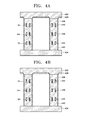
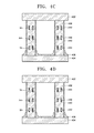
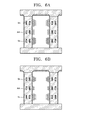
- FIGS. 4A through 4D are cross-sectional views of the structures of a discharge cell included in a PDP having improved structures according to an embodiment of the present invention
- FIG. 5 is a block diagram of an apparatus for driving the PDP according to an embodiment of the present invention.
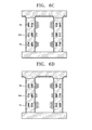
- FIGS. 6A through 6D illustrate distributions of wall charges accumulated by applying driving waveform voltages illustrated in FIG. 3 to the PDP having the improved structures illustrated in FIGS. 4A through 4D;
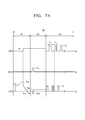
- FIG. 7A illustrates a driving waveform for the PDP having the improved structures of FIGS. 4A through 4D according to a first embodiment of the present invention
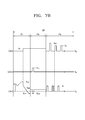
- FIG. 7B illustrates a driving waveform for a PDP having an improved structures of FIGS. 4A through 4D according to a second embodiment of the present invention
- FIGS. 8A through 8D illustrate distributions of wall charges accumulated by applying driving waveform voltages illustrated in FIG. 7A or 7B to the PDP having the improved structure illustrated in FIGS. 4A through 4D;
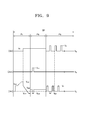
- FIG. 9 illustrates a driving waveform for a PDP having an improved structures of FIGS. 4A through 4D according to a third embodiment of the present invention.
- FIG. 1 is a partially exploded perspective view of a PDP.
- the PDP has a front panel and a rear panel.
- the front panel includes a front substrate 102, a plurality of common electrodes 112 each including a transparent electrode 112a and a bus electrode 112b, a plurality of scan electrodes 114 each including a transparent electrode 114a and a bus electrode 114b, a dielectric layer 109a, and a protection layer 110.
- the rear panel includes a rear substrate 104, a plurality of address electrodes 116, a dielectric layer 109b, a plurality of barrier ribs 106, and a phosphor layer 108.
- the front substrate 102 and rear substrate 104 are spaced apart from each other and face each other.
- a space between the front and rear substrates 102 and 104 is partitioned by the barrier ribs 106 into a plurality of discharge cells.
- a dielectric substance is included near the discharge cells to achieve a panel capacitance.
- the discharge cells can be similarly formed using the panel capacitance and a panel capacitor combined with electrodes surrounding the discharge cells.
- FIG. 2 is a cross-sectional view of the structure of a discharge cell of the PDP of FIG. 1.
- a front substrate 202, a rear substrate 204, barrier ribs 206, a phosphor layer 208, dielectric layers 209a and 209b, protection layer 210, common electrodes 212, 212a, and 212b, scan electrodes 214, 214a, and 214b, and address electrodes 216 are shown in a cross section.
- FIG. 3 is a timing diagram of a part of driving waveform voltages applied to the common electrodes, the scan electrodes, and the address electrodes of the PDP illustrated in FIGS. 1 and 2.
- An address display separation (ADS) scheme is a method of driving a PDP.
- a unit frame is divided into a plurality of sub-fields SF to display an image on the PDP.
- Each of the sub-fields SF includes a reset period Pr, an address period Pa, and a sustain discharge period Ps.
- different driving waveform voltages are applied to each of the common electrodes, the scan electrodes, and the address electrodes of FIGS. 1 and 2.
- a ramp type reset pulse voltage is applied to a scan electrode Yn.
- a scan pulse voltage P_scan is applied to a scan electrode Yn and an address pulse voltage P_address is applied to an address electrode Am.
- sustain pulse voltages P_1, P_2, P_3, and P_4 are alternately applied to a common electrode Xn and the scan electrode Yn.
- the PDP of FIGS. 1 and 2 has low optical transmission characteristics (only about 60%) with regard to visible rays passing through the front substrate, since the visible rays generated by exciting the phosphor must pass through a pair of sustain discharge electrodes 112, 114, the dielectric layer 109a, and the protection layer 110 of the front substrate 102 in order to pass through the front substrate 102.
- the PDP of FIGS. 1 and 2 also has low light-emitting efficiency since the pair of sustain discharge electrodes 112, 114 are disposed in the front of the discharge cells including the front and rear sides thereof. A sustain discharge between the pair of sustain discharge electrodes 112, 114 occurs only at the front of the discharge cells, so that the discharge space is not efficiently used. Also, charged particles generated by the sustain discharge occurring at the front of the discharge cells ion-sputter the phosphor layer at the rear of the discharge cell, causing a permanent afterimage.
- a PDP has been developed that has an improved structure in which the pair of sustain discharge electrodes disposed in the front of the discharge cell is disposed on a barrier rib forming the sides of the discharge cell.
- the PDP having the improved structure has a different electrode structure from the PDP illustrated in FIGS. 1 and 2. Therefore, unexpected problems may occur when the driving waveform voltages illustrated in FIG. 3 are applied to such a structure. Therefore, what is needed is an improved structure for a plasma display device and improved waveforms for driving the electrodes of the improved plasma display device that overcome these problems.
- FIGS. 4A through 4D are cross-sectional views of the structure of a discharge cell included in a plasma display panel (PDP) having an improved structure according to an embodiment of the present invention.
- the PDP having the improved structure includes a front substrate 402, a rear substrate 404, barrier ribs 406, a phosphor layer 408, a protection layer 410, common electrodes or X electrodes 412 Xn, scan electrodes or Y electrodes 414 Yn, and address electrodes or A electrodes 416 Am.
- the space between the front substrate 402 and the rear substrate 404 is divided by barrier ribs 406 into unit discharge cells where discharges occur.
- Each discharge cell includes a front side (a front substrate side), a rear side (a rear substrate side), and barrier rib sides.
- the X electrodes 412, the A electrodes 416, and the Y electrodes 414 of the PDP having the improved structure are disposed within the barrier ribs located between the discharge cells.
- the discharge cell having the structure as illustrated in FIGS. 4A through 4D has a good optical transmissivity of visible rays. Since the electrodes 412, 414, and 416 are disposed within the barrier ribs between the discharge cells, the discharge space of the discharge cells can be efficiently used, thus increasing light-emitting efficiency. Further, since the phosphor layer 408 in each case of FIGS. 4A through 4D is not located between any of the electrodes, the electric field produced by charged particles which are created by a sustain discharge between the pair of the sustain discharge electrodes 412 and 414 does not damage the phosphor layer 408, thus reducing ion-sputtering.
- the PDPs of FIGS. 4A through 4D vary according to 1) the relative positioning of the X, Y and A electrodes as well as 2) the location of the phosphor layer 408.
- the X electrodes are situated closer to the front substrate 402 than either the A or the Y electrodes
- the Y electrodes are situated closer to the rear substrate 404 than either of the X and the A electrodes and the A electrode is located between the X and the Y electrode.
- the X electrode is situated closer to the rear substrate 404 than either the A or the Y electrodes
- the Y electrode is situated closer to the front substrate 402 than either of the X and the A electrodes and the A electrode is located between the X and the Y electrode.
- the phosphor layer 408 is located on the front substrate 402 while in FIGS. 4C and 4D, the phosphor layer 408 is located on the rear substrate 404.
- discharge gas pressure below about 0.5 atmospheres
- discharge gas particles collide with charges due to an electric field produced by driving voltages applied to each of the electrodes of the discharge cells, which results in a plasma discharge, thus producing vacuum ultraviolet radiation.
- the discharge gas is a mixture of xenon (Xe) and one or two among neon (Ne), helium (He), and argon (Ar).
- the barrier ribs 406 partition the space between front substrate 402 and rear substrate 404 into a plurality of discharge cells, each discharge cell being a basic unit of an image.
- the barrier ribs 406 serve to prevent cross talk between adjoining discharge cells.
- a dielectric substance may be formed on the barrier ribs 406 or the barrier ribs can be made out of a dielectric substance.
- the dielectric substance is used as an insulation coating film for the X electrodes 412, the A electrodes 416, and the Y electrodes 414 situated within the barrier ribs 406.
- Some charges produced by a discharge are accumulated on the protection layer 410 over the dielectric substance by electro magnetism according to polarities of voltages applied to each of the electrodes, thus forming wall charges.
- a wall charge voltage produced by the wall charges can be added to driving voltages applied to each of the electrodes in order to determine an electric field present within the discharge space of the discharge cells.
- a stable discharge can occur only when the electric field within the discharge cell is sufficient.
- the barrier ribs 406 can be manufactured to separately include the dielectric substance used as the insulation coating film of each of the electrodes.
- the PDP having the improved structure includes barrier ribs 406 either made out of a dielectric substance or containing a separate dielectric layer.
- a photoluminescence (PL) mechanism which emits visible rays upon being excited by vacuum ultra violet (VUV) light produced by the discharge, occurs in the phosphor layers 408.
- the phosphor layers 408 includes red light-emitting phosphor layers, green light-emitting phosphor layers, and blue light-emitting phosphor layers so that the PDP can realize a visible color image. These three colored phosphor layers are disposed within the discharge cells to form unit pixels.
- the red light-emitting phosphor layers contain (Y,Gd)BO 3 :Eu 3+ , etc.
- the green light-emitting phosphor layers contain Zn 2 SiO 4 :Mn 2+ , etc.
- the blue light-emitting phosphor layers contain BaMgAl 10 O 17 :Eu 2+ , etc.
- the protection layer 410 protects the dielectric substance or the dielectric layer accociated with the barrier ribs and allows the discharge to occur more easily by increasing the emission of secondary electrons.
- the protection layer 410 is formed of magnesium oxide (MgO), etc.
- a side section obtained by cutting the discharge cells of the PDP having the improved structure parallel to the front side and the rear side and perpendicular to the sides of the barrier ribs can result in the shape of a circle or polygon such as a tetragon, a hexagon or an octagon, etc.
- a circular shaped side section of the discharge cells indicates that the discharge cells have a cylindrical shape.
- a polygonal shaped side section of the discharge cell indicates that the discharge cells have a hexahedron shape.
- the cylindrical shape is more advantageous than the hexahedron shape in terms of the discharge efficiency since the cylindrical shape can more efficiently use the discharge space within the discharge cells than the hexahedron shape.
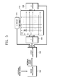
- FIG. 5 is a block diagram of an apparatus for driving the PDP according to an embodiment of the present invention.
- the apparatus for driving the PDP includes an image processor 502, a logic controller 504, an X electrode driver 506, a Y electrode driver 508, and an A electrode driver 510.
- the apparatus further includes a plasma display panel 512 in which a plurality of X electrodes X 1 - Xn, a plurality of Y electrodes Y 1 - Yn, and a plurality of A electrodes A 1 - Am are disposed to cross each other.
- the X electrodes Xn and the Y electrodes Yn are parallel to each other. However, strictly speaking, the X electrodes X 1 - Xn and the Y electrodes Y 1 - Yn are vertically (based on the surface) displaced from each other, which can be seen in FIGS. 4A through 4D.
- the image processor 502 converts an external analog image signal, such as a PC signal, a DVD signal, a video signal, a TV signal, etc. into a digital signal. Image processor 502 image-processes the converted digital signal, generates an internal image signal, and transmits the generated internal image signal to the logic controller 504.
- the internal image signal includes red (R), green (G), and blue (B) image data, a clock signal, and vertical and horizontal synchronization signals.
- the logic controller 504 generates an X electrode driver control signals S X , a Y electrode driver control signals S Y , and an A electrode driver control signals S A by processing a gamma correction, which is an automatic power control (APC) for the internal image signal received from the image processor 502.
- a gamma correction which is an automatic power control (APC) for the internal image signal received from the image processor 502.
- the generated X electrode driver control signals S X , Y electrode driver control signals S Y , and A electrode driver control signals S A are transmitted to the X electrode driver 506, the Y electrode driver 508, and the A electrode driver 510, respectively.
- the X electrode driver 506 receives the X electrode driver control signals S X from the logic controller 504, outputs an X electrode driver driving signals, and applies the X electrode driving voltages to the X electrodes X 1 - Xn of the PDP.
- the Y electrode driver 508 receives the Y electrode driver control signals S Y from the logic controller 504, outputs the Y electrode driver driving signals, and applies Y electrode driving voltages to the Y electrodes Y 1 - Yn of the PDP.
- the A electrode driver 510 receives the A electrode driver control signals S A from the logic controller 504, outputs A electrode driver driving signals, and applies A electrode driving voltages to the A electrodes A 1 - Am of the PDP.
- the plasma display panel 512 includes the X electrodes X 1 - Xn, the Y electrodes Y 1 - Yn, and the A electrodes A 1 - Am which are disposed to overlap each other.
- the plasma display panel 512 displays an image corresponding to an external image signal input to a plasma display device. The image is displayed by visible rays produced in the discharge cells by applying the X, Y, and A electrode driving voltages to the X, Y, and A electrodes Xn, Yn, and Am, respectively.
- Driving waveform voltages which are applied to each of the X, Y, and A electrodes X 1 - Xn, Y 1 - Yn, and A 1 - Am of the PDP 512, will later be described with reference to FIGS. 7A, 7B, and 9.
- FIGS. 6A through 6D illustrate distributions of wall charges accumulated at different points in time in the sub-field by applying the driving waveform voltages illustrated in FIG. 3 to the PDP having the improved structure of FIGS. 4A through 4D. Distributions of wall charges of FIGS. 6A through 6D will now be described with reference to FIG. 3.
- FIG. 6A illustrates a distribution of wall charges around each of the electrodes at the end of an address period (at the end of P A ).
- an X electrode first voltage Vx is applied to the X electrodes Xn.
- a waveform scan pulse voltage is applied to the Y electrodes, the pulse varying from V ya1 to V ya2 during a ramp up, a Y electrode address second voltage V ya2 having a higher electric potential than the Y electrode address first voltage V ya1 previously established, V ya1 being less than Vs applied in the sustain discharge period.
- a waveform address pulse voltage that varies from ground voltage Vg to Vaa, which is higher voltage than the ground voltage Vg previously established, is applied to the A electrodes Am during the address period.
- the voltages applied to each of the electrodes are added to a wall charges accumulated around the each of the electrodes at the end of a reset period (at the end of Pr) to determine the electric field present in the discharge space of the discharge cells.
- an address discharge is generated between the Y electrodes Yn and the A electrodes Am during address period P a .
- Charges produced by the discharge are accumulated around the electrodes to which a voltage having an opposite polarity is applied to form wall charges as illustrated in FIG. 6A. This results in a large quantity of negative wall charges formed around the X electrodes Xn, a small quantity of negative wall charges formed around the A electrodes Am, and a large quantity of positive wall charges formed around the Y electrodes Yn.
- FIG. 6B illustrates a distribution of wall charges around each of the electrodes at the end of a first sustain discharge in the sustain discharge period Ps.
- a first sustain discharge first pulse applied to either the X or the Y electrodes
- the ground voltage Vg is applied to the X electrodes Xn
- a sustain discharge voltage Vs is applied to the Y electrodes Yn which are oppose to the X electrodes Xn
- the ground voltage Vg is applied to the A electrodes Am.
- the voltages applied to each of the electrodes are added to a wall charge voltage accumulated around each of the corresponding electrodes at the end of the address period (at the end of Pa) to determine the electric field present in the discharge spaces of the discharge cells.
- an address discharge between the Y electrodes Yn and the A electrodes Am results in a first sustain discharge between the X electrodes Xn and the Y electrodes Yn.
- Charges generated by the first sustain discharge are accumulated around each of the electrodes and have a polarity that is opposite to the voltages applied thereto.
- a sustain waveform pulse voltage that generates the first sustain discharge can not successfully generate subsequent sustain discharges because of the quantity of wall charges accumulated at the end of the first sustain discharge.
- the sustain discharges after a second sustain discharge in a sustain discharge period are essentially discharges between the X electrodes Xn and the Y electrodes Yn along with a weak start discharge generated using the A electrodes Am.
- the sustain discharge voltage Vs is applied to the X electrodes Xn and the ground voltage Vg is applied to the Y electrodes Yn while wall charges are present from the end of the first sustain discharge.
- FIG. 6C illustrates a distribution of wall charges around each of the electrodes at the end of the second sustain discharge in the sustain discharge period Ps
- FIG. 6D illustrates a distribution of wall charges around each of the electrodes at the end of the third sustain discharge in the sustain discharge period Ps when the waveforms of FIG. 3 are applied to the structures of FIGS. 4A through 4D.
- the second sustain discharge is generated without forming a sufficiently strong electric field between the X electrodes Xn and the Y electrodes Yn.
- This insufficient electric field during the second sustain discharge pulse does not guarantee a stable second sustain discharge between the X electrodes Xn and the Y electrodes Yn, and results in a chain reaction in that all of the subsequent discharges also can be unstable because the electric field is insufficient because of insufficient wall charges present. This chain reaction occurs because a weak or unstable discharge leaves behind insufficient wall charges for the next sustain discharge pulse.
- the second sustain discharge becomes unstable and the wall charges remaining after this unstable discharge P_2 are insufficient for the third discharge P_3.
- the driving voltage as illustrated in FIG. 3 are applied to the X electrodes Xn and the Y electrodes Yn when the wall charges present are as illustrated in FIG. 6C
- the third sustain discharge also becomes unstable, and the wall charges present after the unstable third sustain discharge, as illustrated in FIG. 6D, is also insufficient to produce a stable discharge when pulse P_4 of FIG. 3 is applied to the X and the Y electrodes of FIGS. 4A through 4D.
- each embodiment modifies voltages applied to the electrodes during the second sustain discharge of the sustain address period by adding an extra kick not present in the waveforms of the second sustain discharge pulse of FIG. 3.
- the first embodiment contemplates increasing the pulse width of the first sustain pulse applied to the X electrodes Xn (i.e., the second discharge pulse for the sustain discharge period) as illustrated in FIG. 7A.
- the second embodiment of the present invention contemplates increasing the electric potential applied to the X electrodes during the first sustain pulse applied to the X electrode as illustrated in FIG. 7B.
- the third embodiment contemplates modifying an electric potential of a sustain pulse applied to the Y electrodes as illustrated in FIG. 9 during the second sustain pulse of the sustain discharge period.
- FIG. 7A illustrates a novel driving waveform of the PDP having the improved structure of FIGS. 4A through 4D according to a first embodiment of the present invention
- FIG. 7B illustrates another novel driving waveform of a PDP having the improved structure of FIGS. 4A through 4D according to a second embodiment of the present invention.
- FIGS. 7A and 7B are different from FIG. 3 during the second sustain pulse of the sustain discharge period Ps.
- a step type waveform voltage that rises from the ground voltage Vg to an X electrode first voltage Vx is applied to the X electrodes Xn
- the ground voltage Vg is applied to the A electrodes Am
- a ramp type reset pulse voltage having a rising ramp type waveform voltage and a falling ramp type waveform voltage is applied to the Y electrodes Yn.
- the rising ramp type waveform voltage rises from a Y electrode reset first voltage V yr1 having a higher electric potential than the ground voltage Vg to a Y electrode reset second voltage V yr2 having a higher electric potential than the Y electrode reset first voltage V yr1 .
- the falling ramp type waveform voltage falls from the Y electrode reset first voltage V yr1 having a higher electric potential than the ground voltage Vg to a Y electrode reset third voltage V yr3 having a lower electric potential than Vg.
- the X electrode first voltage Vx having a higher electric potential than the ground voltage Vg is still applied to the X electrodes Xn, an address pulse voltage having a positive pulse waveform of voltage Vaa is applied to the A electrodes Am, and a scan pulse voltage having a negative pulse waveform of voltage V ya2 is applied to the Y electrodes Yn.
- the potential of the A electrode rises from Vg to Vaa while the voltage of the Y electrode falls from Vya1 to Vya2 (the scan pulse).
- a pulse waveform voltage having alternately a low level voltage Vg and a high level voltage Vs is applied to the X electrodes Xn
- a pulse waveform voltage having alternately the high level voltage Vs and the low level voltage Vg is applied to the Y electrodes Yn.
- a high level driving voltage Vs has a longer pulse width T2 than the pulse width Ts of all of the other pulses in period Ps.
- this second pulse in period Ps has a larger pulse width T2 than that of FIG. 3 and than that of the other pulses in period Ps.
- the pulse width Ts is still applied to pulses subsequent to the second pulse of the period Ps as well as to the first pulse of the period Ps.
- a pulse waveform voltage having alternately a low level voltage Vg and a high level voltage Vs is applied to the X electrodes Xn, and a pulse waveform voltage having alternately the high level voltage Vs and the low level voltage Vg is applied to the Y electrodes Yn.
- a period (a period corresponding to period P_2 of FIG. 3, i.e.
- Vx2 high level driving voltage
- the magnitude of the voltage applied to the X electrodes is increased over that of FIG. 3 and over that of other pulses applied during period Ps in FIG. 7B from Vs to Vx2 to increase the electric field within the discharge cells to a sufficient level so that the second discharge in period Ps can be stable.
- an electric potential of high level voltages after a second high level voltage applied to the X electrodes can be equal to an electric potential of high level voltages of FIG. 3.
- the ground voltage Vg having the same electric potential as the low level voltage is applied to the A electrodes Am.
- FIGS. 8A through 8D illustrate distributions of wall charges at different points of time during the sub-field SF accumulated when driving waveform voltages illustrated in FIGS. 7A or 7B are applied to the PDP having the improved structure illustrated in FIGS. 4A through 4D.
- FIG. 8A illustrates a distribution of wall charges around each of the electrodes at the end of the address period Pa
- FIG. 8B illustrates a distribution of wall charges around each of the electrodes at the end of a first sustain discharge in the sustain discharge period Ps.
- the distribution of wall charges illustrated in FIG. 8A is identical to the distribution of wall charges illustrated in FIG. 6A
- the distribution of wall charges as illustrated in FIG. 8B is identical to the distribution of wall charges as illustrated in FIG. 6B.
- the high level driving voltage having the longer pulse width T2 as illustrated in FIG. 7A is applied to the X electrodes Xn, or the high level driving voltage having a higher electric potential Vx2 as illustrated in FIG. 7B is applied to the X electrode Xn during the second sustain discharge of the sustain discharge period Ps.
- the enhanced voltage waveforms in the second sustain pulse produce an electric field sufficient to guarantee a stable second discharge and then produce even more wall charges for the subsequent third discharge. By doing so, the bad chain reaction of FIGS. 6C and 6D is avoided.
- FIG. 8C illustrates a distribution of wall charges around each of the electrodes at the end of the second sustain discharge of the sustain discharge period Ps. If the stable second sustain discharge is generated by applying the high level driving voltage having the long application time T2 as illustrated in FIG. 7A or the high level driving voltage having a high electric potential Vx2 as illustrated in FIG. 7B to the X electrodes Xn when the wall charges as illustrated in FIG. 8B are present, wall charges generated during the second discharge accumulate around the electrodes with a polarity opposite to that of the voltages applied to the electrodes. The resultant is a larger quantity of negative wall charges are formed around the X electrodes Xn in FIG. 8C than in FIG.
- wall charges are sufficiently accumulated in FIG. 8C as after the second and subsequent discharges as compared with the wall charges accumulated in FIG. 6C, to allow for stable subsequent discharges. Since the second stable sustain discharge results in an accumulation of a sufficient amount of wall charges around each of the electrodes for the third discharge, subsequent sustain discharges can occur stably without modification to the voltage waveforms of the third or subsequent sustain discharge pulses in the sustain discharge period Ps. Since these subsequent stable discharges also leave a legacy of sufficient and enhanced wall charges of FIGS. 8C and 8D, the stage is set for even more stable discharges within period Ps and the chain reaction of FIGS. 6C and 6D is avoided. FIG.
- FIG. 8D illustrates a distribution of wall charges around each of the electrodes at the end of the third sustain discharge of the sustain discharge period Ps. Referring to FIG. 8D, a sufficient amount of wall charges are accumulated as illustrated in FIG. 8C. Such a stable effect sets the stage for a stable fourth sustain discharge.
- FIG. 9 illustrates a driving waveform of a PDP having an improved structure according to a third embodiment of the present invention.
- the driving waveforms illustrated in FIG. 9 and FIG. 7A or 7B are identical to each other in regard to the reset period Pr and the address period Pa.
- the driving waveforms applied to the Y electrodes Yn as illustrated in FIG. 9 and FIG. 7A or 7B are different from each other in regard to the second sustain discharge of the sustain discharge period Ps. Specifically, during the second discharge of period Ps in FIG. 9, although the voltage pulse applied to the X electrode is identical to that of P_2 in FIG.
- a small negative voltage Vy2 is simultaneously applied to the Y electrode so that the potential difference between the X and the Y electrodes increases leading to an enhanced electric field within the discharge cells.
- This small negative voltage Vy2 applied to the Y electrodes during the second sustain discharge when the X electrodes are applied high level voltage Vs is enough to prevent the chain reaction of FIGS. 6C and 6D from starting so that the discharges can continue to be stable and the accumulation of wall charges after the discharges are sufficient for more stable discharges, as in FIGS. 8C and 8D.
- a first low level driving voltage Vy2 having a lower electric potential than a second low level voltage Vg is applied to the Y electrodes Yn by not increasing (as illustrated in FIG.
- the electric potential of a sustain pulse voltage applied to the Y electrodes for an electric potential of a low level voltage is reduced.
- the PDP having the improved structure makes it possible to generate stable sustain discharges after the second sustain discharge, thus increasing display quality of the PDP.
Landscapes
- Engineering & Computer Science (AREA)
- Physics & Mathematics (AREA)
- Plasma & Fusion (AREA)
- Power Engineering (AREA)
- Computer Hardware Design (AREA)
- General Physics & Mathematics (AREA)
- Theoretical Computer Science (AREA)
- Chemical & Material Sciences (AREA)
- Materials Engineering (AREA)
- Control Of Indicators Other Than Cathode Ray Tubes (AREA)
- Control Of Gas Discharge Display Tubes (AREA)
- Gas-Filled Discharge Tubes (AREA)
Applications Claiming Priority (1)
| Application Number | Priority Date | Filing Date | Title |
|---|---|---|---|
| KR1020050050140A KR100708691B1 (ko) | 2005-06-11 | 2005-06-11 | 플라즈마 디스플레이 패널의 구동 방법 및 그 구동 방법에의해 구동되는 플라즈마 디스플레이 패널 |
Publications (2)
| Publication Number | Publication Date |
|---|---|
| EP1732057A2 true EP1732057A2 (de) | 2006-12-13 |
| EP1732057A3 EP1732057A3 (de) | 2007-02-07 |
Family
ID=36675898
Family Applications (1)
| Application Number | Title | Priority Date | Filing Date |
|---|---|---|---|
| EP06115201A Withdrawn EP1732057A3 (de) | 2005-06-11 | 2006-06-09 | Verfahren zur Ansteuerung einer Plasmaanzeigetafel (PDP) und damit angesteuerte PDP |
Country Status (5)
| Country | Link |
|---|---|
| US (1) | US7808515B2 (de) |
| EP (1) | EP1732057A3 (de) |
| JP (1) | JP4537340B2 (de) |
| KR (1) | KR100708691B1 (de) |
| CN (1) | CN1877674A (de) |
Families Citing this family (2)
| Publication number | Priority date | Publication date | Assignee | Title |
|---|---|---|---|---|
| JP4374006B2 (ja) * | 2006-09-01 | 2009-12-02 | 日立プラズマディスプレイ株式会社 | プラズマディスプレイパネル駆動方法及びプラズマディスプレイ装置 |
| TWI419106B (zh) * | 2009-05-20 | 2013-12-11 | Au Optronics Corp | 電位移轉器、液晶顯示裝置及電荷分享方法 |
Citations (9)
| Publication number | Priority date | Publication date | Assignee | Title |
|---|---|---|---|---|
| EP0866439A1 (de) | 1997-03-18 | 1998-09-23 | Fujitsu Limited | Verfahren zur Rücksetzung einer Wechselstromplasmaanzeigetafel |
| US6292159B1 (en) | 1997-05-08 | 2001-09-18 | Mitsubishi Denki Kabushiki Kaisha | Method for driving plasma display panel |
| US20020054002A1 (en) | 2000-05-25 | 2002-05-09 | Pioneer Corporation | Method for driving a plasma display panel |
| EP1246156A1 (de) | 2001-03-26 | 2002-10-02 | Lg Electronics Inc. | Verfahren zur Ansteuerung eines Plasmabildschirms mit selektiver Steuerungsumkehrung |
| US20020195963A1 (en) | 2001-05-29 | 2002-12-26 | Pioneer Corporation | Method and apparatus for driving a plasma display panel |
| US20050078061A1 (en) | 2003-09-22 | 2005-04-14 | Jin-Sung Kim | Plasma display panel driving method and plasma display |
| EP1528588A2 (de) | 2003-10-29 | 2005-05-04 | Samsung SDI Co., Ltd. | Plasmaanzeigetafel |
| EP1530193A2 (de) | 2003-11-08 | 2005-05-11 | Lg Electronics Inc. | Verfahren und Vorrichtung zur Ansteuerung einer Plasmaanzeige |
| US20050116466A1 (en) | 2003-12-02 | 2005-06-02 | Massimo Arosio | Flat-surface quick coupling tubes extending between a pressurized fluid user device and a fluid feeding means |
Family Cites Families (31)
| Publication number | Priority date | Publication date | Assignee | Title |
|---|---|---|---|---|
| JP2917279B2 (ja) | 1988-11-30 | 1999-07-12 | 富士通株式会社 | ガス放電パネル |
| JP3259253B2 (ja) | 1990-11-28 | 2002-02-25 | 富士通株式会社 | フラット型表示装置の階調駆動方法及び階調駆動装置 |
| US6097357A (en) | 1990-11-28 | 2000-08-01 | Fujitsu Limited | Full color surface discharge type plasma display device |
| EP1231590A3 (de) | 1991-12-20 | 2003-08-06 | Fujitsu Limited | Vorrichtung zur Steuerung einer Anzeigetafel |
| EP0554172B1 (de) | 1992-01-28 | 1998-04-29 | Fujitsu Limited | Plasma Farbanzeige-Vorrichtung von Oberflächenentladungs-Typ |
| JP3025598B2 (ja) | 1993-04-30 | 2000-03-27 | 富士通株式会社 | 表示駆動装置及び表示駆動方法 |
| JP2891280B2 (ja) | 1993-12-10 | 1999-05-17 | 富士通株式会社 | 平面表示装置の駆動装置及び駆動方法 |
| JPH07186719A (ja) * | 1993-12-27 | 1995-07-25 | Shiroki Corp | ミラー付きサンバイザー及びその製造方法 |
| JPH0934397A (ja) * | 1995-07-24 | 1997-02-07 | Fujitsu Ltd | プラズマ・ディスプレイ・パネル |
| JP3163563B2 (ja) | 1995-08-25 | 2001-05-08 | 富士通株式会社 | 面放電型プラズマ・ディスプレイ・パネル及びその製造方法 |
| JP2845183B2 (ja) | 1995-10-20 | 1999-01-13 | 富士通株式会社 | ガス放電パネル |
| JP3457173B2 (ja) * | 1997-03-18 | 2003-10-14 | 富士通株式会社 | プラズマディスプレイパネルの駆動方法 |
| JP3028075B2 (ja) * | 1997-05-30 | 2000-04-04 | 日本電気株式会社 | プラズマディスプレイパネルの駆動方法 |
| JP3424587B2 (ja) | 1998-06-18 | 2003-07-07 | 富士通株式会社 | プラズマディスプレイパネルの駆動方法 |
| TW527576B (en) * | 1998-07-29 | 2003-04-11 | Hitachi Ltd | Display panel driving method and discharge type display apparatus |
| JP3466098B2 (ja) * | 1998-11-20 | 2003-11-10 | 富士通株式会社 | ガス放電パネルの駆動方法 |
| JP2000305517A (ja) | 1999-04-22 | 2000-11-02 | Pioneer Electronic Corp | プラズマディスプレイパネルの駆動方法 |
| JP4030685B2 (ja) | 1999-07-30 | 2008-01-09 | 三星エスディアイ株式会社 | プラズマディスプレイおよびその製造方法 |
| US6603448B2 (en) * | 1999-12-16 | 2003-08-05 | Matsushita Electric Industrial Co., Ltd | Plasma display panel |
| JP2001228820A (ja) | 2000-02-14 | 2001-08-24 | Mitsubishi Electric Corp | プラズマディスプレイパネルの駆動方法及びプラズマディスプレイ装置 |
| JP2001325888A (ja) | 2000-03-09 | 2001-11-22 | Samsung Yokohama Research Institute Co Ltd | プラズマディスプレイ及びその製造方法 |
| JP4528449B2 (ja) * | 2001-01-12 | 2010-08-18 | 日立プラズマディスプレイ株式会社 | プラズマディスプレイパネルの駆動方法及び表示装置 |
| JP2002351396A (ja) * | 2001-05-30 | 2002-12-06 | Matsushita Electric Ind Co Ltd | プラズマディスプレイパネルの駆動方法 |
| JP2004004513A (ja) | 2002-04-25 | 2004-01-08 | Fujitsu Hitachi Plasma Display Ltd | プラズマディスプレイパネルの駆動方法およびプラズマディスプレイ装置 |
| JP2004349058A (ja) * | 2003-05-21 | 2004-12-09 | Pioneer Electronic Corp | プラズマディスプレイパネル |
| JP4419429B2 (ja) * | 2003-05-08 | 2010-02-24 | パナソニック株式会社 | 表示装置 |
| JP4385117B2 (ja) * | 2003-07-17 | 2009-12-16 | パナソニック株式会社 | プラズマディスプレイパネルの駆動方法 |
| KR20050038932A (ko) * | 2003-10-23 | 2005-04-29 | 삼성에스디아이 주식회사 | 플라즈마 디스플레이 패널의 구동 방법 및 플라즈마 표시장치 |
| KR20050040558A (ko) * | 2003-10-29 | 2005-05-03 | 삼성에스디아이 주식회사 | 플라즈마 디스플레이 패널의 구동 방법 및 플라즈마 표시장치 |
| KR100603324B1 (ko) | 2003-11-29 | 2006-07-20 | 삼성에스디아이 주식회사 | 플라즈마 디스플레이 패널 |
| JP4577681B2 (ja) * | 2004-07-30 | 2010-11-10 | 株式会社日立プラズマパテントライセンシング | プラズマディスプレイパネルの駆動方法 |
-
2005
- 2005-06-11 KR KR1020050050140A patent/KR100708691B1/ko not_active Expired - Fee Related
-
2006
- 2006-04-03 JP JP2006102419A patent/JP4537340B2/ja not_active Expired - Fee Related
- 2006-06-01 US US11/444,409 patent/US7808515B2/en not_active Expired - Fee Related
- 2006-06-09 EP EP06115201A patent/EP1732057A3/de not_active Withdrawn
- 2006-06-12 CN CNA2006100927022A patent/CN1877674A/zh active Pending
Patent Citations (9)
| Publication number | Priority date | Publication date | Assignee | Title |
|---|---|---|---|---|
| EP0866439A1 (de) | 1997-03-18 | 1998-09-23 | Fujitsu Limited | Verfahren zur Rücksetzung einer Wechselstromplasmaanzeigetafel |
| US6292159B1 (en) | 1997-05-08 | 2001-09-18 | Mitsubishi Denki Kabushiki Kaisha | Method for driving plasma display panel |
| US20020054002A1 (en) | 2000-05-25 | 2002-05-09 | Pioneer Corporation | Method for driving a plasma display panel |
| EP1246156A1 (de) | 2001-03-26 | 2002-10-02 | Lg Electronics Inc. | Verfahren zur Ansteuerung eines Plasmabildschirms mit selektiver Steuerungsumkehrung |
| US20020195963A1 (en) | 2001-05-29 | 2002-12-26 | Pioneer Corporation | Method and apparatus for driving a plasma display panel |
| US20050078061A1 (en) | 2003-09-22 | 2005-04-14 | Jin-Sung Kim | Plasma display panel driving method and plasma display |
| EP1528588A2 (de) | 2003-10-29 | 2005-05-04 | Samsung SDI Co., Ltd. | Plasmaanzeigetafel |
| EP1530193A2 (de) | 2003-11-08 | 2005-05-11 | Lg Electronics Inc. | Verfahren und Vorrichtung zur Ansteuerung einer Plasmaanzeige |
| US20050116466A1 (en) | 2003-12-02 | 2005-06-02 | Massimo Arosio | Flat-surface quick coupling tubes extending between a pressurized fluid user device and a fluid feeding means |
Also Published As
| Publication number | Publication date |
|---|---|
| KR100708691B1 (ko) | 2007-04-17 |
| KR20060128585A (ko) | 2006-12-14 |
| JP2006350298A (ja) | 2006-12-28 |
| JP4537340B2 (ja) | 2010-09-01 |
| CN1877674A (zh) | 2006-12-13 |
| EP1732057A3 (de) | 2007-02-07 |
| US7808515B2 (en) | 2010-10-05 |
| US20060279485A1 (en) | 2006-12-14 |
Similar Documents
| Publication | Publication Date | Title |
|---|---|---|
| JP2003263127A (ja) | プラズマディスプレイ装置 | |
| JP2005141257A (ja) | プラズマディスプレーパネルの駆動方法 | |
| JP4124764B2 (ja) | プラズマディスプレイパネルの駆動方法 | |
| US8212745B2 (en) | Method for driving a plasma display panel using subfield groups | |
| US7808515B2 (en) | Method of driving plasma display panel (PDP) and PDP driven using the method | |
| US8212746B2 (en) | Method for driving a plasma display panel by using a holding period between subfield groups | |
| US20060001610A1 (en) | Plasma display panel (PDP) | |
| JP2009009163A (ja) | プラズマディスプレイパネルの駆動方法 | |
| US7692387B2 (en) | Plasma display panel | |
| US20060001608A1 (en) | Plasma display panel (PDP) | |
| US7623095B2 (en) | Plasma display panel (PDP) | |
| US20070035475A1 (en) | Method of driving plasma display panel and plasma display apparatus driven using the method | |
| US20070152913A1 (en) | Driving method for significantly reducing addressing time in plasma display panel | |
| KR100581934B1 (ko) | 플라즈마 디스플레이 패널 | |
| KR100647679B1 (ko) | 플라즈마 디스플레이 패널 구동방법 | |
| KR100615252B1 (ko) | 플라즈마 디스플레이 패널 | |
| US20070035476A1 (en) | Method of driving plasma display panel and plasma display device driven using the method | |
| KR100389021B1 (ko) | 고주파 플라즈마 디스플레이 패널의 구동방법 | |
| KR100794348B1 (ko) | 플라즈마 디스플레이 장치 | |
| KR20000021115A (ko) | 플라즈마 디스플레이 패널의 구동방법 | |
| JP2008097045A (ja) | プラズマディスプレイパネルの駆動方法 | |
| JP2008015057A (ja) | プラズマディスプレイ装置 | |
| US20070222713A1 (en) | Method of driving plasma display panel | |
| US20060284797A1 (en) | Plasma display panel (PDP) | |
| KR20070097192A (ko) | 플라즈마 디스플레이 패널 |
Legal Events
| Date | Code | Title | Description |
|---|---|---|---|
| PUAI | Public reference made under article 153(3) epc to a published international application that has entered the european phase |
Free format text: ORIGINAL CODE: 0009012 |
|
| 17P | Request for examination filed |
Effective date: 20060609 |
|
| AK | Designated contracting states |
Kind code of ref document: A2 Designated state(s): AT BE BG CH CY CZ DE DK EE ES FI FR GB GR HU IE IS IT LI LT LU LV MC NL PL PT RO SE SI SK TR |
|
| AX | Request for extension of the european patent |
Extension state: AL BA HR MK YU |
|
| PUAL | Search report despatched |
Free format text: ORIGINAL CODE: 0009013 |
|
| AK | Designated contracting states |
Kind code of ref document: A3 Designated state(s): AT BE BG CH CY CZ DE DK EE ES FI FR GB GR HU IE IS IT LI LT LU LV MC NL PL PT RO SE SI SK TR |
|
| AX | Request for extension of the european patent |
Extension state: AL BA HR MK YU |
|
| 17Q | First examination report despatched |
Effective date: 20070611 |
|
| AKX | Designation fees paid |
Designated state(s): DE FR GB NL |
|
| GRAP | Despatch of communication of intention to grant a patent |
Free format text: ORIGINAL CODE: EPIDOSNIGR1 |
|
| STAA | Information on the status of an ep patent application or granted ep patent |
Free format text: STATUS: THE APPLICATION IS DEEMED TO BE WITHDRAWN |
|
| 18D | Application deemed to be withdrawn |
Effective date: 20110219 |