EP1734800A2 - Technique de fabrication d'un ensemble électronique surmoulé - Google Patents
Technique de fabrication d'un ensemble électronique surmoulé Download PDFInfo
- Publication number
- EP1734800A2 EP1734800A2 EP06076163A EP06076163A EP1734800A2 EP 1734800 A2 EP1734800 A2 EP 1734800A2 EP 06076163 A EP06076163 A EP 06076163A EP 06076163 A EP06076163 A EP 06076163A EP 1734800 A2 EP1734800 A2 EP 1734800A2
- Authority
- EP
- European Patent Office
- Prior art keywords
- backplate
- substrate
- die
- cavity
- assembly
- Prior art date
- Legal status (The legal status is an assumption and is not a legal conclusion. Google has not performed a legal analysis and makes no representation as to the accuracy of the status listed.)
- Granted
Links
Images



Classifications
-
- H—ELECTRICITY
- H10—SEMICONDUCTOR DEVICES; ELECTRIC SOLID-STATE DEVICES NOT OTHERWISE PROVIDED FOR
- H10W—GENERIC PACKAGES, INTERCONNECTIONS, CONNECTORS OR OTHER CONSTRUCTIONAL DETAILS OF DEVICES COVERED BY CLASS H10
- H10W74/00—Encapsulations, e.g. protective coatings
- H10W74/10—Encapsulations, e.g. protective coatings characterised by their shape or disposition
- H10W74/111—Encapsulations, e.g. protective coatings characterised by their shape or disposition the semiconductor body being completely enclosed
- H10W74/114—Encapsulations, e.g. protective coatings characterised by their shape or disposition the semiconductor body being completely enclosed by a substrate and the encapsulations
-
- H—ELECTRICITY
- H05—ELECTRIC TECHNIQUES NOT OTHERWISE PROVIDED FOR
- H05K—PRINTED CIRCUITS; CASINGS OR CONSTRUCTIONAL DETAILS OF ELECTRIC APPARATUS; MANUFACTURE OF ASSEMBLAGES OF ELECTRICAL COMPONENTS
- H05K1/00—Printed circuits
- H05K1/02—Details
- H05K1/0201—Thermal arrangements, e.g. for cooling, heating or preventing overheating
- H05K1/0203—Cooling of mounted components
-
- H—ELECTRICITY
- H05—ELECTRIC TECHNIQUES NOT OTHERWISE PROVIDED FOR
- H05K—PRINTED CIRCUITS; CASINGS OR CONSTRUCTIONAL DETAILS OF ELECTRIC APPARATUS; MANUFACTURE OF ASSEMBLAGES OF ELECTRICAL COMPONENTS
- H05K3/00—Apparatus or processes for manufacturing printed circuits
- H05K3/22—Secondary treatment of printed circuits
- H05K3/28—Applying non-metallic protective coatings
- H05K3/284—Applying non-metallic protective coatings for encapsulating mounted components
-
- H—ELECTRICITY
- H05—ELECTRIC TECHNIQUES NOT OTHERWISE PROVIDED FOR
- H05K—PRINTED CIRCUITS; CASINGS OR CONSTRUCTIONAL DETAILS OF ELECTRIC APPARATUS; MANUFACTURE OF ASSEMBLAGES OF ELECTRICAL COMPONENTS
- H05K5/00—Casings, cabinets or drawers for electric apparatus
- H05K5/0026—Casings, cabinets or drawers for electric apparatus provided with connectors and printed circuit boards [PCB], e.g. automotive electronic control units
- H05K5/0034—Casings, cabinets or drawers for electric apparatus provided with connectors and printed circuit boards [PCB], e.g. automotive electronic control units having an overmolded housing covering the PCB
-
- H—ELECTRICITY
- H05—ELECTRIC TECHNIQUES NOT OTHERWISE PROVIDED FOR
- H05K—PRINTED CIRCUITS; CASINGS OR CONSTRUCTIONAL DETAILS OF ELECTRIC APPARATUS; MANUFACTURE OF ASSEMBLAGES OF ELECTRICAL COMPONENTS
- H05K7/00—Constructional details common to different types of electric apparatus
- H05K7/20—Modifications to facilitate cooling, ventilating, or heating
- H05K7/20845—Modifications to facilitate cooling, ventilating, or heating for automotive electronic casings
- H05K7/20854—Heat transfer by conduction from internal heat source to heat radiating structure
-
- H—ELECTRICITY
- H10—SEMICONDUCTOR DEVICES; ELECTRIC SOLID-STATE DEVICES NOT OTHERWISE PROVIDED FOR
- H10W—GENERIC PACKAGES, INTERCONNECTIONS, CONNECTORS OR OTHER CONSTRUCTIONAL DETAILS OF DEVICES COVERED BY CLASS H10
- H10W40/00—Arrangements for thermal protection or thermal control
- H10W40/70—Fillings or auxiliary members in containers or in encapsulations for thermal protection or control
- H10W40/77—Auxiliary members characterised by their shape
- H10W40/778—Auxiliary members characterised by their shape in encapsulations
-
- H—ELECTRICITY
- H10—SEMICONDUCTOR DEVICES; ELECTRIC SOLID-STATE DEVICES NOT OTHERWISE PROVIDED FOR
- H10W—GENERIC PACKAGES, INTERCONNECTIONS, CONNECTORS OR OTHER CONSTRUCTIONAL DETAILS OF DEVICES COVERED BY CLASS H10
- H10W90/00—Package configurations
-
- H—ELECTRICITY
- H05—ELECTRIC TECHNIQUES NOT OTHERWISE PROVIDED FOR
- H05K—PRINTED CIRCUITS; CASINGS OR CONSTRUCTIONAL DETAILS OF ELECTRIC APPARATUS; MANUFACTURE OF ASSEMBLAGES OF ELECTRICAL COMPONENTS
- H05K2201/00—Indexing scheme relating to printed circuits covered by H05K1/00
- H05K2201/09—Shape and layout
- H05K2201/09009—Substrate related
- H05K2201/09063—Holes or slots in insulating substrate not used for electrical connections
-
- H—ELECTRICITY
- H05—ELECTRIC TECHNIQUES NOT OTHERWISE PROVIDED FOR
- H05K—PRINTED CIRCUITS; CASINGS OR CONSTRUCTIONAL DETAILS OF ELECTRIC APPARATUS; MANUFACTURE OF ASSEMBLAGES OF ELECTRICAL COMPONENTS
- H05K2201/00—Indexing scheme relating to printed circuits covered by H05K1/00
- H05K2201/09—Shape and layout
- H05K2201/09209—Shape and layout details of conductors
- H05K2201/09654—Shape and layout details of conductors covering at least two types of conductors provided for in H05K2201/09218 - H05K2201/095
- H05K2201/09745—Recess in conductor, e.g. in pad or in metallic substrate
-
- H—ELECTRICITY
- H05—ELECTRIC TECHNIQUES NOT OTHERWISE PROVIDED FOR
- H05K—PRINTED CIRCUITS; CASINGS OR CONSTRUCTIONAL DETAILS OF ELECTRIC APPARATUS; MANUFACTURE OF ASSEMBLAGES OF ELECTRICAL COMPONENTS
- H05K2201/00—Indexing scheme relating to printed circuits covered by H05K1/00
- H05K2201/10—Details of components or other objects attached to or integrated in a printed circuit board
- H05K2201/10007—Types of components
- H05K2201/10189—Non-printed connector
-
- H—ELECTRICITY
- H05—ELECTRIC TECHNIQUES NOT OTHERWISE PROVIDED FOR
- H05K—PRINTED CIRCUITS; CASINGS OR CONSTRUCTIONAL DETAILS OF ELECTRIC APPARATUS; MANUFACTURE OF ASSEMBLAGES OF ELECTRICAL COMPONENTS
- H05K2201/00—Indexing scheme relating to printed circuits covered by H05K1/00
- H05K2201/10—Details of components or other objects attached to or integrated in a printed circuit board
- H05K2201/10431—Details of mounted components
- H05K2201/1056—Metal over component, i.e. metal plate over component mounted on or embedded in PCB
-
- H—ELECTRICITY
- H05—ELECTRIC TECHNIQUES NOT OTHERWISE PROVIDED FOR
- H05K—PRINTED CIRCUITS; CASINGS OR CONSTRUCTIONAL DETAILS OF ELECTRIC APPARATUS; MANUFACTURE OF ASSEMBLAGES OF ELECTRICAL COMPONENTS
- H05K2201/00—Indexing scheme relating to printed circuits covered by H05K1/00
- H05K2201/10—Details of components or other objects attached to or integrated in a printed circuit board
- H05K2201/10613—Details of electrical connections of non-printed components, e.g. special leads
- H05K2201/10621—Components characterised by their electrical contacts
- H05K2201/10674—Flip chip
-
- H—ELECTRICITY
- H05—ELECTRIC TECHNIQUES NOT OTHERWISE PROVIDED FOR
- H05K—PRINTED CIRCUITS; CASINGS OR CONSTRUCTIONAL DETAILS OF ELECTRIC APPARATUS; MANUFACTURE OF ASSEMBLAGES OF ELECTRICAL COMPONENTS
- H05K2203/00—Indexing scheme relating to apparatus or processes for manufacturing printed circuits covered by H05K3/00
- H05K2203/13—Moulding and encapsulation; Deposition techniques; Protective layers
- H05K2203/1305—Moulding and encapsulation
- H05K2203/1316—Moulded encapsulation of mounted components
-
- H—ELECTRICITY
- H05—ELECTRIC TECHNIQUES NOT OTHERWISE PROVIDED FOR
- H05K—PRINTED CIRCUITS; CASINGS OR CONSTRUCTIONAL DETAILS OF ELECTRIC APPARATUS; MANUFACTURE OF ASSEMBLAGES OF ELECTRICAL COMPONENTS
- H05K3/00—Apparatus or processes for manufacturing printed circuits
- H05K3/0058—Laminating printed circuit boards onto other substrates, e.g. metallic substrates
- H05K3/0061—Laminating printed circuit boards onto other substrates, e.g. metallic substrates onto a metallic substrate, e.g. a heat sink
-
- H—ELECTRICITY
- H10—SEMICONDUCTOR DEVICES; ELECTRIC SOLID-STATE DEVICES NOT OTHERWISE PROVIDED FOR
- H10W—GENERIC PACKAGES, INTERCONNECTIONS, CONNECTORS OR OTHER CONSTRUCTIONAL DETAILS OF DEVICES COVERED BY CLASS H10
- H10W72/00—Interconnections or connectors in packages
- H10W72/071—Connecting or disconnecting
- H10W72/072—Connecting or disconnecting of bump connectors
- H10W72/07251—Connecting or disconnecting of bump connectors characterised by changes in properties of the bump connectors during connecting
-
- H—ELECTRICITY
- H10—SEMICONDUCTOR DEVICES; ELECTRIC SOLID-STATE DEVICES NOT OTHERWISE PROVIDED FOR
- H10W—GENERIC PACKAGES, INTERCONNECTIONS, CONNECTORS OR OTHER CONSTRUCTIONAL DETAILS OF DEVICES COVERED BY CLASS H10
- H10W72/00—Interconnections or connectors in packages
- H10W72/20—Bump connectors, e.g. solder bumps or copper pillars; Dummy bumps; Thermal bumps
-
- H—ELECTRICITY
- H10—SEMICONDUCTOR DEVICES; ELECTRIC SOLID-STATE DEVICES NOT OTHERWISE PROVIDED FOR
- H10W—GENERIC PACKAGES, INTERCONNECTIONS, CONNECTORS OR OTHER CONSTRUCTIONAL DETAILS OF DEVICES COVERED BY CLASS H10
- H10W72/00—Interconnections or connectors in packages
- H10W72/90—Bond pads, in general
-
- H—ELECTRICITY
- H10—SEMICONDUCTOR DEVICES; ELECTRIC SOLID-STATE DEVICES NOT OTHERWISE PROVIDED FOR
- H10W—GENERIC PACKAGES, INTERCONNECTIONS, CONNECTORS OR OTHER CONSTRUCTIONAL DETAILS OF DEVICES COVERED BY CLASS H10
- H10W72/00—Interconnections or connectors in packages
- H10W72/90—Bond pads, in general
- H10W72/921—Structures or relative sizes of bond pads
- H10W72/923—Bond pads having multiple stacked layers
-
- H—ELECTRICITY
- H10—SEMICONDUCTOR DEVICES; ELECTRIC SOLID-STATE DEVICES NOT OTHERWISE PROVIDED FOR
- H10W—GENERIC PACKAGES, INTERCONNECTIONS, CONNECTORS OR OTHER CONSTRUCTIONAL DETAILS OF DEVICES COVERED BY CLASS H10
- H10W72/00—Interconnections or connectors in packages
- H10W72/90—Bond pads, in general
- H10W72/941—Dispositions of bond pads
- H10W72/9415—Dispositions of bond pads relative to the surface, e.g. recessed, protruding
Definitions
- the present invention is generally directed to an electronic assembly and, more specifically, to a technique for manufacturing an overmolded electronic assembly.
- an overmolded electronic assembly 100 that includes a single-sided substrate 104, e.g., a printed circuit board (PCB), is depicted. As shown, the assembly 100 also includes a backplate 102, which provides rigidity for the PCB 104, during the overmolding process. A plurality of connector pins 110 are connected to conductive traces of the PCB 104, to provide electrical connection to an external device.
- a single-sided substrate 104 e.g., a printed circuit board (PCB)
- PCB printed circuit board
- IC die 106A Electrically connected to the PCB 104 is an integrated circuit (IC) die 106A, e.g., a flip-chip, an IC die 106B, e.g., a flip-chip, a ball grid array (BGA) 106C, a discrete component 132 and a plurality of surface mount components 130, e.g., resistors and capacitors, all of which are implemented to provide a desired functionality.
- IC die 106A e.g., a flip-chip
- IC die 106B e.g., a flip-chip
- BGA ball grid array
- surface mount components 130 e.g., resistors and capacitors, all of which are implemented to provide a desired functionality.
- An overmold material 150 encloses the PCB 104 (and its associated components) and at least a portion of the backplate 102.
- Solder bumps 107 are utilized to electrically connect contacts 111 of the flip-chips 106A and 106B and the BGA 106C to electrically conductive traces 109, formed on a surface of the PCB 104. It should be appreciated that since only one side of the PCB 104 is populated, the assembly 100 generally requires a larger product form factor than would be required if a double-side PCB was implemented. This, in turn, results in a requirement that the PCB and the backplate have a larger area, which, in turn, leads to increased cost. Additionally, heatsinking the flip-chips 106A and 106B of the assembly 100 is generally more difficult, as the flip-chips 106A and 106B are located on the side of the PCB 104 that is opposite the backplate 102.
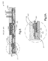
- flip-chips 206A and 206B are located on the same side of a PCB 204 that is contact with a heatsink 202. Similar to the electronic assembly 100 of Fig. 1, the flip-chips 206A and 206B and the BGA 206C include contacts 209, which are coupled to electrically conductive traces 207 (formed on the PCB 204) by solder bumps 211, during a solder reflow process.
- the electronic assembly 200 includes a plurality of electronic components 230 and the BGA 206C that are coupled to electrically conductive traces formed on a second side of the PCB 204. While the assembly 200 of Fig. 2 can be produced with a reduced size, as compared to the assembly 100 of Fig. 1, the PCB 204 is not as well supported during the overmold process, as compared to the PCB 104 of the assembly 100 of Fig. 1.
- connector pins 210 extend from the second side of the PCB 204 to provide electrical connection to an external device. It should also be appreciated that the assembly 200 of Fig. 2 may also not adequately support the connector pins 210 during the overmold process and, as such, deflection of the PCB 204 may lead to potential damage to the connector pin solder joints.
- a technique for manufacturing an electronic assembly includes a number of steps. Initially, a backplate that includes a cavity, formed into a first side of the backplate, is provided. Next, a substrate with a first side of an integrated circuit (IC) die mounted to a first side of the substrate is provided. The IC die is electrically connected to one or more of a plurality of electrically conductive traces formed on the first side of the substrate. The substrate includes a hole approximate an outer edge of the IC die. The first side of the substrate is then positioned in contact with at least a portion of the first side of the backplate. The IC die is positioned within the cavity with a second side of the IC die in thermal contact with the backplate. The substrate and at least a portion of the backplate are overmolded with an overmold material, which enters the cavity through the hole to substantially underfill the IC die and substantially fill an unoccupied portion of the cavity.
- IC integrated circuit
- the substrate is a printed circuit board (PCB).
- the substrate includes an electrical connector, whose pins extend through an aperture in the backplate, to provide electrical interconnection to an external device.
- the IC die is a flip-chip.
- the technique includes the additional step of providing an electrically non-conductive adhesive between at least a portion of the first side of the backplate and the first side of the substrate.
- the adhesive may be an acrylic adhesive and the backplate may be made of aluminum.
- the technique includes the step of providing a thermal film between the second side of the IC die and the first side of the backplate.
- the thermal film may be an Indium film.
- an electronic assembly which includes a double-sided substrate, exhibits many of the advantages of an electronic assembly that implements a single-sided substrate.
- a substrate may be mounted to an aluminum backplate using an acrylic adhesive, e.g., Part No. VHB F-9473PC, manufactured and made commercially available by 3M.
- the substrate is primarily a single-sided assembly that includes certain electronic components, e.g., power integrated circuits (ICs) and surface mount filter capacitors, mounted on a backplate side of the substrate.
- ICs power integrated circuits
- surface mount filter capacitors mounted on a backplate side of the substrate.
- the VHB adhesive tape provides a continuous bond, which distributes stresses along most of the surface of the substrate, and provides strength and durability in extreme applications. Furthermore, with flip-chips mounted on the heatsink side of the substrate, heatsinking can be readily achieved to enhance thermal conductivity of the assembly. As more of the substrate is supported during the overmolding process, solder joint stress of the assembly is generally reduced.
- An assembly configured according to the present invention provides increased package density, as compared to assemblies implementing single-sided substrates, as flip-chips and other surface mount technology (SMT) devices may be mounted on a backplate side of the substrate.
- SMT surface mount technology
- an assembly constructed according to the present invention utilizes less substrate materials, backplate materials and molding compound, as compared to prior art electronic assemblies implementing single-sided substrates.
- thermal films such as an Indium film, flip-chip heatsinking may be optimized and manufacturing yield of the product may be increased.
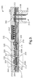
- the assembly 300 includes a backplate 302 and a substrate 304, e.g., a printed circuit board (PCB).
- the substrate 304 is connected to the backplate 302, with an adhesive 312, such as that disclosed above, manufactured and made commercially available by 3M.
- the backplate 302 includes a plurality of cavities 319, which receive flip-chips 306A and 306B, which are mounted to a first side of the substrate 304.
- a thermal film 314 is located between a second side of the flip-chips 306A and 306B and the first side of the backplate 302 in the cavity 319 area.
- a ball grid array (BGA) 306C is mounted to electrically conductive traces located on a second side of the PCB 304. Additionally, a number of other electronic components 330 and 332 are mounted on the second side of the substrate 304.
- a connector 310 includes a plurality of pins 310 retained in a connector housing 310B. As is shown, an overmold material 350 has underfilled the flip-chips 306A and 306B and has filled the cavities 319. The filling of the cavities 319 by the material 350 is facilitated by holes 320 in the PCB 304.
- the holes 320 facilitate entry of the overmold material 350 into the cavities 319, to allow for substantial underfill of the IC dies 306A and 306B, and filling of the cavities 319.
- a portion 360 of the assembly 300 is shown in an enlarged view.
- a backplate 302 is provided that includes a cavity 319 and an aperture 340.
- a substrate 304 is provided that includes integrated circuit (IC) die 306A and 306B, e.g., flip-chips.
- IC integrated circuit
- step 406 the IC die 306A and 306B are positioned in the cavity 319 of the backplate 302 and pins 310A of connector 310 are positioned through the aperture 340 and the pins 310A of the connector 310 are electrically connected to the traces of the substrate 304.
- the substrate 304 and at least a portion of the backplate 302 are overmolded with an overmold material 350.
- an electronic assembly has been described herein that exhibits adequate support in the substrate connector area to prevent deflection and potential damage to connector pin solder joints. Furthermore, the electronic assembly described herein exhibits adequate support around flip-chips mounted to the PCB to prevent solder cracks and readily allow for heatsinking of the flip-chips.
Landscapes
- Engineering & Computer Science (AREA)
- Microelectronics & Electronic Packaging (AREA)
- Manufacturing & Machinery (AREA)
- Physics & Mathematics (AREA)
- Thermal Sciences (AREA)
- Structures For Mounting Electric Components On Printed Circuit Boards (AREA)
- Wire Bonding (AREA)
- Cooling Or The Like Of Semiconductors Or Solid State Devices (AREA)
- Encapsulation Of And Coatings For Semiconductor Or Solid State Devices (AREA)
Applications Claiming Priority (1)
| Application Number | Priority Date | Filing Date | Title |
|---|---|---|---|
| US11/150,997 US7473585B2 (en) | 2005-06-13 | 2005-06-13 | Technique for manufacturing an overmolded electronic assembly |
Publications (3)
| Publication Number | Publication Date |
|---|---|
| EP1734800A2 true EP1734800A2 (fr) | 2006-12-20 |
| EP1734800A3 EP1734800A3 (fr) | 2009-01-21 |
| EP1734800B1 EP1734800B1 (fr) | 2011-08-10 |
Family
ID=37124401
Family Applications (1)
| Application Number | Title | Priority Date | Filing Date |
|---|---|---|---|
| EP06076163A Active EP1734800B1 (fr) | 2005-06-13 | 2006-06-02 | Technique de fabrication d'un ensemble électronique surmoulé |
Country Status (3)
| Country | Link |
|---|---|
| US (1) | US7473585B2 (fr) |
| EP (1) | EP1734800B1 (fr) |
| AT (1) | ATE520291T1 (fr) |
Cited By (7)
| Publication number | Priority date | Publication date | Assignee | Title |
|---|---|---|---|---|
| EP1740027A3 (fr) * | 2005-06-27 | 2009-06-03 | Delphi Technologies, Inc. | Procédé de fabrication d'un assemblage électronique surmoulé |
| WO2016112980A1 (fr) * | 2015-01-15 | 2016-07-21 | Pierburg Pump Technology Gmbh | Groupe auxiliaire électrique de véhicule automobile |
| WO2017077193A1 (fr) * | 2015-11-06 | 2017-05-11 | Tactotek Oy | Structure multicouche et procédé associé pour la fabrication de composants électroniques |
| WO2018182810A1 (fr) * | 2017-03-27 | 2018-10-04 | Raytheon Company | Isolation thermique de composants cryo-refroidis depuis des cartes de circuit ou autres structures |
| WO2018206296A1 (fr) * | 2017-05-08 | 2018-11-15 | Robert Bosch Gmbh | Module électronique et procédé de fabrication |
| WO2018233899A1 (fr) * | 2017-06-19 | 2018-12-27 | Robert Bosch Gmbh | Module électronique |
| WO2021047957A1 (fr) * | 2019-09-11 | 2021-03-18 | Vitesco Technologies Germany Gmbh | Dispositif de commande pour véhicule automobile |
Families Citing this family (22)
| Publication number | Priority date | Publication date | Assignee | Title |
|---|---|---|---|---|
| US7440282B2 (en) * | 2006-05-16 | 2008-10-21 | Delphi Technologies, Inc. | Heat sink electronic package having compliant pedestal |
| US20090091889A1 (en) * | 2007-10-09 | 2009-04-09 | Oman Todd P | Power electronic module having improved heat dissipation capability |
| DE102008008386A1 (de) * | 2008-02-09 | 2009-08-13 | Airbus Deutschland Gmbh | Verfahren zur Herstellung eines FVW-Bauteils |
| US8234034B2 (en) | 2009-06-26 | 2012-07-31 | Autoliv Asp, Inc. | Enhanced electronic assembly |
| JP2011100718A (ja) * | 2009-10-05 | 2011-05-19 | Yazaki Corp | コネクタ |
| US8228682B1 (en) | 2010-08-20 | 2012-07-24 | Xilinx, Inc. | Electronic assembly with trenches for underfill material |
| US8914183B2 (en) | 2010-09-20 | 2014-12-16 | Joshua Forwerck | Enhanced electronic assembly |
| DE102011088969A1 (de) * | 2011-12-19 | 2013-06-20 | Robert Bosch Gmbh | Getriebesteuermodul |
| US9552977B2 (en) * | 2012-12-10 | 2017-01-24 | Intel Corporation | Landside stiffening capacitors to enable ultrathin and other low-Z products |
| US9623591B2 (en) | 2013-01-15 | 2017-04-18 | Basf Se | Method of encapsulating an electronic component |
| KR101449271B1 (ko) * | 2013-04-19 | 2014-10-08 | 현대오트론 주식회사 | 오버몰딩을 이용한 차량의 전자 제어 장치 및 그 제조 방법 |
| KR101428933B1 (ko) * | 2013-07-05 | 2014-08-08 | 현대오트론 주식회사 | 방열판을 이용한 차량의 전자 제어 장치 및 그 제조 방법 |
| DE102013215368B4 (de) * | 2013-08-05 | 2025-06-05 | Zf Friedrichshafen Ag | Elektronische Einheit mit Leiterplatte |
| US9579511B2 (en) | 2014-12-15 | 2017-02-28 | Medtronic, Inc. | Medical device with surface mounted lead connector |
| DE102015207867A1 (de) * | 2015-04-29 | 2016-11-03 | Robert Bosch Gmbh | Elektronische Baugruppe, insbesondere für ein Getriebesteuermodul |
| JP6591234B2 (ja) * | 2015-08-21 | 2019-10-16 | ルネサスエレクトロニクス株式会社 | 半導体装置 |
| US9780077B2 (en) * | 2015-09-10 | 2017-10-03 | Nxp Usa, Inc. | System-in-packages containing preassembled surface mount device modules and methods for the production thereof |
| JP6561129B2 (ja) * | 2015-09-29 | 2019-08-14 | 日立オートモティブシステムズ株式会社 | 電子制御装置またはその製造方法 |
| CN114402701B (zh) * | 2019-09-11 | 2025-04-18 | 纬湃科技德国有限责任公司 | 机动车辆的控制设备和用于制造和测量控制设备的密封性的方法 |
| DE102019213962A1 (de) * | 2019-09-13 | 2021-03-18 | Vitesco Technologies Germany Gmbh | Getriebesteuergerät, Kraftfahrzeug und Verfahren zur Umspritzung einer Leiterplatte eines Getriebesteuergeräts |
| DE102021213703A1 (de) | 2021-12-02 | 2023-06-07 | Zf Friedrichshafen Ag | Verfahren zur Herstellung einer Baugruppe |
| US11991869B2 (en) * | 2022-10-11 | 2024-05-21 | Lunar Energy, Inc. | Thermal management system including an overmolded layer and a conductive layer over a circuit board |
Citations (2)
| Publication number | Priority date | Publication date | Assignee | Title |
|---|---|---|---|---|
| EP0641154A1 (fr) | 1993-08-30 | 1995-03-01 | TEMIC TELEFUNKEN microelectronic GmbH | Boîtier pour composants électroniques |
| US6307749B1 (en) | 2000-10-23 | 2001-10-23 | Delphi Technologies, Inc. | Overmolded electronic module with underfilled surface-mount components |
Family Cites Families (12)
| Publication number | Priority date | Publication date | Assignee | Title |
|---|---|---|---|---|
| US4679463A (en) | 1984-08-31 | 1987-07-14 | Nissan Motor Co., Ltd. | Limited slip differential |
| JPH03243421A (ja) | 1990-02-19 | 1991-10-30 | Mazda Motor Corp | 車両の動力伝達装置 |
| US5310388A (en) | 1993-02-10 | 1994-05-10 | Asha Corporation | Vehicle drivetrain hydraulic coupling |
| US6180045B1 (en) * | 1998-05-20 | 2001-01-30 | Delco Electronics Corporation | Method of forming an overmolded electronic assembly |
| US7062537B2 (en) | 2002-11-25 | 2006-06-13 | Microsoft Corporation | Workflow services architecture |
| US20040148299A1 (en) | 2002-11-25 | 2004-07-29 | Microsoft Corporation | Automated workflow composable action model |
| US6833628B2 (en) * | 2002-12-17 | 2004-12-21 | Delphi Technologies, Inc. | Mutli-chip module |
| US6873040B2 (en) * | 2003-07-08 | 2005-03-29 | Texas Instruments Incorporated | Semiconductor packages for enhanced number of terminals, speed and power performance |
| US7132746B2 (en) * | 2003-08-18 | 2006-11-07 | Delphi Technologies, Inc. | Electronic assembly with solder-bonded heat sink |
| US7134194B2 (en) * | 2003-11-13 | 2006-11-14 | Delphi Technologies, Inc. | Method of developing an electronic module |
| JP4311243B2 (ja) * | 2004-03-15 | 2009-08-12 | 株式会社デンソー | 電子機器 |
| US7268429B2 (en) | 2005-06-27 | 2007-09-11 | Delphi Technologies, Inc. | Technique for manufacturing an overmolded electronic assembly |
-
2005
- 2005-06-13 US US11/150,997 patent/US7473585B2/en not_active Expired - Lifetime
-
2006
- 2006-06-02 AT AT06076163T patent/ATE520291T1/de not_active IP Right Cessation
- 2006-06-02 EP EP06076163A patent/EP1734800B1/fr active Active
Patent Citations (2)
| Publication number | Priority date | Publication date | Assignee | Title |
|---|---|---|---|---|
| EP0641154A1 (fr) | 1993-08-30 | 1995-03-01 | TEMIC TELEFUNKEN microelectronic GmbH | Boîtier pour composants électroniques |
| US6307749B1 (en) | 2000-10-23 | 2001-10-23 | Delphi Technologies, Inc. | Overmolded electronic module with underfilled surface-mount components |
Cited By (19)
| Publication number | Priority date | Publication date | Assignee | Title |
|---|---|---|---|---|
| EP1740027A3 (fr) * | 2005-06-27 | 2009-06-03 | Delphi Technologies, Inc. | Procédé de fabrication d'un assemblage électronique surmoulé |
| WO2016112980A1 (fr) * | 2015-01-15 | 2016-07-21 | Pierburg Pump Technology Gmbh | Groupe auxiliaire électrique de véhicule automobile |
| WO2017077193A1 (fr) * | 2015-11-06 | 2017-05-11 | Tactotek Oy | Structure multicouche et procédé associé pour la fabrication de composants électroniques |
| US9801273B2 (en) | 2015-11-06 | 2017-10-24 | Tactotek Oy | Multilayer structure and related method of manufacture for electronics |
| TWI742218B (zh) * | 2017-03-27 | 2021-10-11 | 美商雷神公司 | 低溫冷卻元件與電路板或其它結構之熱隔離技術 |
| WO2018182810A1 (fr) * | 2017-03-27 | 2018-10-04 | Raytheon Company | Isolation thermique de composants cryo-refroidis depuis des cartes de circuit ou autres structures |
| IL268001B2 (en) * | 2017-03-27 | 2023-03-01 | Raytheon Co | Thermal insulation of printed circuit components or other cryogenically cooled structures |
| US10390455B2 (en) | 2017-03-27 | 2019-08-20 | Raytheon Company | Thermal isolation of cryo-cooled components from circuit boards or other structures |
| IL268001B (en) * | 2017-03-27 | 2022-11-01 | Raytheon Co | Thermal isolation of cryo-cooled components from circuit boards or other structures |
| CN110603693B (zh) * | 2017-05-08 | 2021-09-03 | 罗伯特·博世有限公司 | 电子模块和制造方法 |
| WO2018206296A1 (fr) * | 2017-05-08 | 2018-11-15 | Robert Bosch Gmbh | Module électronique et procédé de fabrication |
| CN110603693A (zh) * | 2017-05-08 | 2019-12-20 | 罗伯特·博世有限公司 | 电子模块和制造方法 |
| CN110754139A (zh) * | 2017-06-19 | 2020-02-04 | 罗伯特·博世有限公司 | 电子模块 |
| CN110754139B (zh) * | 2017-06-19 | 2022-08-26 | 罗伯特·博世有限公司 | 电子模块 |
| WO2018233899A1 (fr) * | 2017-06-19 | 2018-12-27 | Robert Bosch Gmbh | Module électronique |
| WO2021047957A1 (fr) * | 2019-09-11 | 2021-03-18 | Vitesco Technologies Germany Gmbh | Dispositif de commande pour véhicule automobile |
| CN114342567A (zh) * | 2019-09-11 | 2022-04-12 | 纬湃科技德国有限责任公司 | 用于机动车辆的控制设备 |
| US12200872B2 (en) | 2019-09-11 | 2025-01-14 | Vitesco Technologies Germany Gmbh | Control device for a motor vehicle |
| CN114342567B (zh) * | 2019-09-11 | 2025-03-25 | 纬湃科技德国有限责任公司 | 用于机动车辆的控制设备 |
Also Published As
| Publication number | Publication date |
|---|---|
| US20060281230A1 (en) | 2006-12-14 |
| US7473585B2 (en) | 2009-01-06 |
| ATE520291T1 (de) | 2011-08-15 |
| EP1734800A3 (fr) | 2009-01-21 |
| EP1734800B1 (fr) | 2011-08-10 |
Similar Documents
| Publication | Publication Date | Title |
|---|---|---|
| EP1734800B1 (fr) | Technique de fabrication d'un ensemble électronique surmoulé | |
| US20010046129A1 (en) | Interposer for connecting two substrates and resulting assembly | |
| KR20050026972A (ko) | 백 사이드와 공동 실장된 커패시터들을 갖는 전자패키지와 그 제조 방법 | |
| EP1207727A2 (fr) | Connecteur laminé flexible | |
| KR20040069962A (ko) | 전자 소자 캐리어를 위한 최적화된 덮개의 장착 | |
| US6507118B1 (en) | Multi-metal layer circuit | |
| CN1279821A (zh) | 应力衰减型电子元器件、布线板及其安装体 | |
| EP1076361A2 (fr) | Assemblage de puces avec plots de connexion pour circuits imprimés multicouches | |
| KR20260018010A (ko) | 성형된 비아 및 양면 압입 핀을 갖는 전력 모듈 패키지 및 이를 형성하는 방법 | |
| CN1389005A (zh) | 低成本及高可靠度应用的高可靠度插入物 | |
| US7134194B2 (en) | Method of developing an electronic module | |
| US20030150645A1 (en) | Method and apparatus for coupling a microelectronic device package to a circuit board | |
| CN100527412C (zh) | 电子电路模块及其制造方法 | |
| CN105848415B (zh) | 侧边具有表面黏着型接脚的电路模块以及电路板与系统 | |
| KR100199286B1 (ko) | 홈이 형성된 인쇄 회로 기판을 갖는 칩 스케일 패키지 | |
| EP1748518A2 (fr) | Connecteur à monter sur une surface | |
| JP4016587B2 (ja) | 電子部品及びその製造方法 | |
| WO2008117213A2 (fr) | Ensemble d'au moins deux cartes de circuit imprimé et procédé d'assemblage d'au moins deux cartes de circuit imprimé | |
| US11164804B2 (en) | Integrated circuit (IC) device package lid attach utilizing nano particle metallic paste | |
| JPH08340164A (ja) | Bga型パッケージの面実装構造 | |
| CN108573877B (zh) | 形成贴附式双面载放零件的电子芯片模块的方法 | |
| US20060000718A1 (en) | Substrate plating methods and apparatus | |
| KR100646489B1 (ko) | 반도체 장치 및 그의 제조 방법 | |
| EP1628509A3 (fr) | Module électronique avec support formé in situ | |
| US20060000642A1 (en) | Interposer with compliant pins |
Legal Events
| Date | Code | Title | Description |
|---|---|---|---|
| PUAI | Public reference made under article 153(3) epc to a published international application that has entered the european phase |
Free format text: ORIGINAL CODE: 0009012 |
|
| AK | Designated contracting states |
Kind code of ref document: A2 Designated state(s): AT BE BG CH CY CZ DE DK EE ES FI FR GB GR HU IE IS IT LI LT LU LV MC NL PL PT RO SE SI SK TR |
|
| AX | Request for extension of the european patent |
Extension state: AL BA HR MK YU |
|
| PUAL | Search report despatched |
Free format text: ORIGINAL CODE: 0009013 |
|
| AK | Designated contracting states |
Kind code of ref document: A3 Designated state(s): AT BE BG CH CY CZ DE DK EE ES FI FR GB GR HU IE IS IT LI LT LU LV MC NL PL PT RO SE SI SK TR |
|
| AX | Request for extension of the european patent |
Extension state: AL BA HR MK YU |
|
| 17P | Request for examination filed |
Effective date: 20090721 |
|
| AKX | Designation fees paid |
Designated state(s): AT BE BG CH CY CZ DE DK EE ES FI FR GB GR HU IE IS IT LI LT LU LV MC NL PL PT RO SE SI SK TR |
|
| 17Q | First examination report despatched |
Effective date: 20090901 |
|
| GRAP | Despatch of communication of intention to grant a patent |
Free format text: ORIGINAL CODE: EPIDOSNIGR1 |
|
| GRAS | Grant fee paid |
Free format text: ORIGINAL CODE: EPIDOSNIGR3 |
|
| GRAA | (expected) grant |
Free format text: ORIGINAL CODE: 0009210 |
|
| AK | Designated contracting states |
Kind code of ref document: B1 Designated state(s): AT BE BG CH CY CZ DE DK EE ES FI FR GB GR HU IE IS IT LI LT LU LV MC NL PL PT RO SE SI SK TR |
|
| REG | Reference to a national code |
Ref country code: GB Ref legal event code: FG4D |
|
| REG | Reference to a national code |
Ref country code: CH Ref legal event code: EP |
|
| REG | Reference to a national code |
Ref country code: IE Ref legal event code: FG4D |
|
| REG | Reference to a national code |
Ref country code: DE Ref legal event code: R096 Ref document number: 602006023616 Country of ref document: DE Effective date: 20111013 |
|
| REG | Reference to a national code |
Ref country code: NL Ref legal event code: VDEP Effective date: 20110810 |
|
| LTIE | Lt: invalidation of european patent or patent extension |
Effective date: 20110810 |
|
| PG25 | Lapsed in a contracting state [announced via postgrant information from national office to epo] |
Ref country code: PT Free format text: LAPSE BECAUSE OF FAILURE TO SUBMIT A TRANSLATION OF THE DESCRIPTION OR TO PAY THE FEE WITHIN THE PRESCRIBED TIME-LIMIT Effective date: 20111212 Ref country code: SE Free format text: LAPSE BECAUSE OF FAILURE TO SUBMIT A TRANSLATION OF THE DESCRIPTION OR TO PAY THE FEE WITHIN THE PRESCRIBED TIME-LIMIT Effective date: 20110810 Ref country code: FI Free format text: LAPSE BECAUSE OF FAILURE TO SUBMIT A TRANSLATION OF THE DESCRIPTION OR TO PAY THE FEE WITHIN THE PRESCRIBED TIME-LIMIT Effective date: 20110810 Ref country code: NL Free format text: LAPSE BECAUSE OF FAILURE TO SUBMIT A TRANSLATION OF THE DESCRIPTION OR TO PAY THE FEE WITHIN THE PRESCRIBED TIME-LIMIT Effective date: 20110810 Ref country code: IS Free format text: LAPSE BECAUSE OF FAILURE TO SUBMIT A TRANSLATION OF THE DESCRIPTION OR TO PAY THE FEE WITHIN THE PRESCRIBED TIME-LIMIT Effective date: 20111210 Ref country code: LT Free format text: LAPSE BECAUSE OF FAILURE TO SUBMIT A TRANSLATION OF THE DESCRIPTION OR TO PAY THE FEE WITHIN THE PRESCRIBED TIME-LIMIT Effective date: 20110810 |
|
| REG | Reference to a national code |
Ref country code: AT Ref legal event code: MK05 Ref document number: 520291 Country of ref document: AT Kind code of ref document: T Effective date: 20110810 |
|
| PG25 | Lapsed in a contracting state [announced via postgrant information from national office to epo] |
Ref country code: CY Free format text: LAPSE BECAUSE OF FAILURE TO SUBMIT A TRANSLATION OF THE DESCRIPTION OR TO PAY THE FEE WITHIN THE PRESCRIBED TIME-LIMIT Effective date: 20110810 Ref country code: PL Free format text: LAPSE BECAUSE OF FAILURE TO SUBMIT A TRANSLATION OF THE DESCRIPTION OR TO PAY THE FEE WITHIN THE PRESCRIBED TIME-LIMIT Effective date: 20110810 Ref country code: AT Free format text: LAPSE BECAUSE OF FAILURE TO SUBMIT A TRANSLATION OF THE DESCRIPTION OR TO PAY THE FEE WITHIN THE PRESCRIBED TIME-LIMIT Effective date: 20110810 Ref country code: SI Free format text: LAPSE BECAUSE OF FAILURE TO SUBMIT A TRANSLATION OF THE DESCRIPTION OR TO PAY THE FEE WITHIN THE PRESCRIBED TIME-LIMIT Effective date: 20110810 Ref country code: LV Free format text: LAPSE BECAUSE OF FAILURE TO SUBMIT A TRANSLATION OF THE DESCRIPTION OR TO PAY THE FEE WITHIN THE PRESCRIBED TIME-LIMIT Effective date: 20110810 Ref country code: GR Free format text: LAPSE BECAUSE OF FAILURE TO SUBMIT A TRANSLATION OF THE DESCRIPTION OR TO PAY THE FEE WITHIN THE PRESCRIBED TIME-LIMIT Effective date: 20111111 |
|
| PG25 | Lapsed in a contracting state [announced via postgrant information from national office to epo] |
Ref country code: BE Free format text: LAPSE BECAUSE OF FAILURE TO SUBMIT A TRANSLATION OF THE DESCRIPTION OR TO PAY THE FEE WITHIN THE PRESCRIBED TIME-LIMIT Effective date: 20110810 |
|
| PG25 | Lapsed in a contracting state [announced via postgrant information from national office to epo] |
Ref country code: CZ Free format text: LAPSE BECAUSE OF FAILURE TO SUBMIT A TRANSLATION OF THE DESCRIPTION OR TO PAY THE FEE WITHIN THE PRESCRIBED TIME-LIMIT Effective date: 20110810 Ref country code: SK Free format text: LAPSE BECAUSE OF FAILURE TO SUBMIT A TRANSLATION OF THE DESCRIPTION OR TO PAY THE FEE WITHIN THE PRESCRIBED TIME-LIMIT Effective date: 20110810 |
|
| PG25 | Lapsed in a contracting state [announced via postgrant information from national office to epo] |
Ref country code: EE Free format text: LAPSE BECAUSE OF FAILURE TO SUBMIT A TRANSLATION OF THE DESCRIPTION OR TO PAY THE FEE WITHIN THE PRESCRIBED TIME-LIMIT Effective date: 20110810 Ref country code: RO Free format text: LAPSE BECAUSE OF FAILURE TO SUBMIT A TRANSLATION OF THE DESCRIPTION OR TO PAY THE FEE WITHIN THE PRESCRIBED TIME-LIMIT Effective date: 20110810 Ref country code: IT Free format text: LAPSE BECAUSE OF FAILURE TO SUBMIT A TRANSLATION OF THE DESCRIPTION OR TO PAY THE FEE WITHIN THE PRESCRIBED TIME-LIMIT Effective date: 20110810 |
|
| PLBE | No opposition filed within time limit |
Free format text: ORIGINAL CODE: 0009261 |
|
| STAA | Information on the status of an ep patent application or granted ep patent |
Free format text: STATUS: NO OPPOSITION FILED WITHIN TIME LIMIT |
|
| PG25 | Lapsed in a contracting state [announced via postgrant information from national office to epo] |
Ref country code: DK Free format text: LAPSE BECAUSE OF FAILURE TO SUBMIT A TRANSLATION OF THE DESCRIPTION OR TO PAY THE FEE WITHIN THE PRESCRIBED TIME-LIMIT Effective date: 20110810 |
|
| 26N | No opposition filed |
Effective date: 20120511 |
|
| REG | Reference to a national code |
Ref country code: DE Ref legal event code: R097 Ref document number: 602006023616 Country of ref document: DE Effective date: 20120511 |
|
| PG25 | Lapsed in a contracting state [announced via postgrant information from national office to epo] |
Ref country code: MC Free format text: LAPSE BECAUSE OF NON-PAYMENT OF DUE FEES Effective date: 20120630 |
|
| REG | Reference to a national code |
Ref country code: CH Ref legal event code: PL |
|
| REG | Reference to a national code |
Ref country code: CH Ref legal event code: PL |
|
| REG | Reference to a national code |
Ref country code: IE Ref legal event code: MM4A |
|
| PG25 | Lapsed in a contracting state [announced via postgrant information from national office to epo] |
Ref country code: CH Free format text: LAPSE BECAUSE OF NON-PAYMENT OF DUE FEES Effective date: 20120630 Ref country code: ES Free format text: LAPSE BECAUSE OF FAILURE TO SUBMIT A TRANSLATION OF THE DESCRIPTION OR TO PAY THE FEE WITHIN THE PRESCRIBED TIME-LIMIT Effective date: 20111121 Ref country code: LI Free format text: LAPSE BECAUSE OF NON-PAYMENT OF DUE FEES Effective date: 20120630 Ref country code: IE Free format text: LAPSE BECAUSE OF NON-PAYMENT OF DUE FEES Effective date: 20120602 |
|
| PG25 | Lapsed in a contracting state [announced via postgrant information from national office to epo] |
Ref country code: BG Free format text: LAPSE BECAUSE OF FAILURE TO SUBMIT A TRANSLATION OF THE DESCRIPTION OR TO PAY THE FEE WITHIN THE PRESCRIBED TIME-LIMIT Effective date: 20111110 |
|
| PG25 | Lapsed in a contracting state [announced via postgrant information from national office to epo] |
Ref country code: TR Free format text: LAPSE BECAUSE OF FAILURE TO SUBMIT A TRANSLATION OF THE DESCRIPTION OR TO PAY THE FEE WITHIN THE PRESCRIBED TIME-LIMIT Effective date: 20110810 |
|
| PG25 | Lapsed in a contracting state [announced via postgrant information from national office to epo] |
Ref country code: LU Free format text: LAPSE BECAUSE OF NON-PAYMENT OF DUE FEES Effective date: 20120602 |
|
| PG25 | Lapsed in a contracting state [announced via postgrant information from national office to epo] |
Ref country code: HU Free format text: LAPSE BECAUSE OF FAILURE TO SUBMIT A TRANSLATION OF THE DESCRIPTION OR TO PAY THE FEE WITHIN THE PRESCRIBED TIME-LIMIT Effective date: 20060602 |
|
| REG | Reference to a national code |
Ref country code: FR Ref legal event code: PLFP Year of fee payment: 11 |
|
| REG | Reference to a national code |
Ref country code: FR Ref legal event code: PLFP Year of fee payment: 12 |
|
| REG | Reference to a national code |
Ref country code: FR Ref legal event code: PLFP Year of fee payment: 13 |
|
| REG | Reference to a national code |
Ref country code: DE Ref legal event code: R081 Ref document number: 602006023616 Country of ref document: DE Owner name: DELPHI TECHNOLOGIES IP LIMITED, BB Free format text: FORMER OWNER: DELPHI TECHNOLOGIES, INC., TROY, MICH., US |
|
| REG | Reference to a national code |
Ref country code: GB Ref legal event code: 732E Free format text: REGISTERED BETWEEN 20190214 AND 20190221 |
|
| P01 | Opt-out of the competence of the unified patent court (upc) registered |
Effective date: 20230327 |
|
| PGFP | Annual fee paid to national office [announced via postgrant information from national office to epo] |
Ref country code: DE Payment date: 20250509 Year of fee payment: 20 |
|
| PGFP | Annual fee paid to national office [announced via postgrant information from national office to epo] |
Ref country code: GB Payment date: 20250508 Year of fee payment: 20 |
|
| PGFP | Annual fee paid to national office [announced via postgrant information from national office to epo] |
Ref country code: FR Payment date: 20250512 Year of fee payment: 20 |