EP1736268A2 - Méthode d'usinage d'un matériau semiconducteur en nitrure. - Google Patents
Méthode d'usinage d'un matériau semiconducteur en nitrure. Download PDFInfo
- Publication number
- EP1736268A2 EP1736268A2 EP06011947A EP06011947A EP1736268A2 EP 1736268 A2 EP1736268 A2 EP 1736268A2 EP 06011947 A EP06011947 A EP 06011947A EP 06011947 A EP06011947 A EP 06011947A EP 1736268 A2 EP1736268 A2 EP 1736268A2
- Authority
- EP
- European Patent Office
- Prior art keywords
- nitride semiconductor
- semiconductor crystal
- working
- crystal
- ingot
- Prior art date
- Legal status (The legal status is an assumption and is not a legal conclusion. Google has not performed a legal analysis and makes no representation as to the accuracy of the status listed.)
- Withdrawn
Links
Images

Classifications
-
- H—ELECTRICITY
- H10—SEMICONDUCTOR DEVICES; ELECTRIC SOLID-STATE DEVICES NOT OTHERWISE PROVIDED FOR
- H10P—GENERIC PROCESSES OR APPARATUS FOR THE MANUFACTURE OR TREATMENT OF DEVICES COVERED BY CLASS H10
- H10P52/00—Grinding, lapping or polishing of wafers, substrates or parts of devices
-
- B—PERFORMING OPERATIONS; TRANSPORTING
- B23—MACHINE TOOLS; METAL-WORKING NOT OTHERWISE PROVIDED FOR
- B23H—WORKING OF METAL BY THE ACTION OF A HIGH CONCENTRATION OF ELECTRIC CURRENT ON A WORKPIECE USING AN ELECTRODE WHICH TAKES THE PLACE OF A TOOL; SUCH WORKING COMBINED WITH OTHER FORMS OF WORKING OF METAL
- B23H7/00—Processes or apparatus applicable to both electrical discharge machining and electrochemical machining
- B23H7/02—Wire-cutting
-
- B—PERFORMING OPERATIONS; TRANSPORTING
- B23—MACHINE TOOLS; METAL-WORKING NOT OTHERWISE PROVIDED FOR
- B23H—WORKING OF METAL BY THE ACTION OF A HIGH CONCENTRATION OF ELECTRIC CURRENT ON A WORKPIECE USING AN ELECTRODE WHICH TAKES THE PLACE OF A TOOL; SUCH WORKING COMBINED WITH OTHER FORMS OF WORKING OF METAL
- B23H9/00—Machining specially adapted for treating particular metal objects or for obtaining special effects or results on metal objects
Definitions
- the present invention relates to a method of working a semiconductor crystal, and more particularly to a method of working a nitride semiconductor crystal.
- a cutting tool such as an inner diameter blade or a wire saw is used to cut out a substrate from a semiconductor crystal ingot of silicon or the like.
- a compound semiconductor crystal ingot of GaAs, InP or the like is also cut with a multi-wire saw, as described in Japanese Patent Laying-Open No. 09-017755 , for example.
- a nitride semiconductor crystal of GaN or the like has a wide energy band gap, and thus it is in increasing demand as a semiconductor suitable for an LED (light emitting diode) or an LD (laser diode) capable of emitting short-wavelength light. Accordingly, it is desired to work a grown crystal ingot of a nitride semiconductor in a simple and efficient manner at lower costs.
- the nitride semiconductor crystal of GaN or the like among the compound semiconductors has high hardness and low toughness, it is difficult to cut such a nitride crystal by the same apparatus and method as those used for a Si crystal or a GaAs crystal, and there often arise problems such as crack generation and waviness on a surface formed by cutting (hereinafter referred to as a cut-surface).
- a cut-surface a surface formed by cutting
- the GaN crystal has low toughness, it is liable to cause cracks or fracture.
- the GaN crystal has high hardness and is composed of two elements, distortion due to cutting easily occurs depending on distribution of hardness in the crystal. In order to cut a GaN ingot with a good yield rate, therefore, it is necessary to reduce cutting load, which may cause reduction in throughput.
- a polycrystalline portion (a portion having low crystalline quality) grows in a peripheral region of the semiconductor ingot. Although this peripheral region should be removed, grinding the periphery of the nitride semiconductor ingot is liable to cause cracks.
- the ingot is long, it is also difficult to work the long ingot with a core drill, resulting in severe wear of the tool. Further, since such working needs abrasive grains and a grinding wheel, it requires higher costs. Specifically, residual stress is concentrated in the polycrystalline portion in the peripheral region of the GaN ingot, and thus if balance of the stress is lost during the working, cracks are spontaneously generated due to poor strength of the crystal.
- the core drill is used to work the long ingot, it is difficult for a working fluid to permeate through a position to be worked, whereby making it difficult to provide satisfactory working.
- an object of the present invention is to provide a technique capable of working a nitride semiconductor crystal in a simple and efficient manner at lower costs.
- a method of working a nitride semiconductor crystal when the nitride semiconductor crystal is worked, voltage is applied between the crystal and a tool electrode to cause electrical discharge, so that the crystal is partially removed and worked by local heat generated by the electrical discharge.
- the nitride semiconductor crystal can be cut using a wire electrode as the tool electrode.
- the wire electrode is made of tungsten or molybdenum.
- a nitride semiconductor crystal substrate can be obtained by cutting an ingot of the nitride semiconductor crystal. Further, after cutting the nitride semiconductor crystal, a cut-surface of the crystal can be smoothed by sweeping the cut-surface again with the wire electrode. On the other hand, the nitride semiconductor crystal substrate obtained by the cutting may further be etched. In addition, the nitride semiconductor crystal substrate obtained by the cutting may further be polished.
- a peripheral region of the nitride semiconductor crystal ingot includes a portion having low crystalline quality as compared to an inside region of the ingot
- the ingot including the portion of low crystalline quality can be cut in a direction perpendicular to a direction in which the ingot has grown. Further, unevenness on a grown surface of the nitride semiconductor crystal ingot can be removed to obtain an ingot having a surface with unevenness of less than 30 ⁇ m.
- the nitride semiconductor crystal ingot can be cut so as to separate a peripheral portion thereof having low crystalline quality from a good crystal portion inside the ingot. More specifically, a through-hole is formed in the nitride semiconductor ingot and then the wire electrode is passed through the through-hole to make the through-hole a starting point for cutting in order to take out a good crystal inside the ingot without working the peripheral portion having low crystalline quality.
- an edge at an end of a surface of the nitride semiconductor crystal can also be removed by inclining a longitudinal direction of the wire electrode at an angle in a range of 0-60° from a direction perpendicular to the surface of the nitride semiconductor crystal.
- a desired surface geometry can be formed on the nitride semiconductor crystal by transferring a surface geometry of the tool electrode to the crystal. Furthermore, unevenness on a surface of the nitride semiconductor crystal can be removed to obtain a smooth surface having a surface roughness Ry of less than 10 ⁇ m and a flatness of less than 20 ⁇ m, by using the tool electrode having a surface roughness Ry of less than 10 ⁇ m and a flatness of less than 20 ⁇ m.
- a crystal ingot is grown and then a peripheral portion thereof having low crystalline quality is removed by grinding or with a core drill. Thereafter, the ingot is cut to obtain a slice having a desired thickness. A cut-surface of the slice is polished and etched to be flat whereby removing a work-affected layer, and then the slice is cleaned to remove impurities on the cut-surface.
- an ingot thereof is cut using an inner diameter blade or a wire saw.
- a nitride semiconductor crystal is liable to cause cracks because of its high hardness and low toughness, and since it contains two elemental components, it is difficult to perform linear cutting on an ingot thereof due to distribution of the hardness. While it is effective to perform cutting at low speed with reduced cutting load in order to suppress generation of cracks, it leads to reduction in throughput. Further, although it is also effective for the linear cutting to increase thickness of the tool in order to maintain strength of the tool, it requires an increased cutting allowance of the ingot and thus the resultant material yield rate is reduced. Consequently, with the conventional mechanical cutting technique, it is difficult to simultaneously achieve satisfactory cutting quality and throughput for the nitride semiconductor crystal.
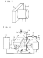
- Fig. 1 is a schematic perspective view illustrating a method of cutting out a substrate from a nitride semiconductor crystal ingot by means of wire electrical discharge machining.
- a nitride semiconductor crystal ingot 1 is fixed to a holder 2 and immersed in a cooling insulative medium such as deionized water or kerosene.
- a wire electrode 3 comes close to ingot 1, and voltage is applied between wire electrode 3 and ingot 1.
- local and minute electrical discharge is generated between wire electrode 3 and ingot 1, and then cutting proceeds as the ingot material is locally removed by heat generated by the electrical discharge.
- wire electrode 3 Since the material of wire electrode 3 is also consumed during the electrical discharge machining, the wire becomes thin at the electrical discharging portion. Accordingly, wire electrode 3 is moved in its longitudinal direction at a constant speed in order to be prevented from locally becoming thin and being broken during the electrical discharge machining. Further, wire 3 and ingot 1 are relatively moved by servo control such that wire 3 cuts into ingot 1 as the cutting proceeds.
- Fig. 2 is a schematic block diagram illustrating an example of an overall structure of such a wire electrical discharge machine. This drawing illustrates the case where a relatively large workpiece is subjected to wire electrical discharge machining.
- a workpiece 1a is fixed on cross tables 11a and 11b which can be driven in an X-axis direction and a Y-axis direction, respectively.
- An X-axis motor 12a is connected to the upper table 11a, and a Y-axis motor 12b is connected to the lower table 11b.
- X-axis motor 12a and Y-axis motor 12b are controlled by an NC (numerically controlling) device 13 which includes a servo circuit.
- a through-hole is formed in workpiece 1a beforehand, and a wire electrode 14 is passed through the through-hole.
- wire 14 is supplied from a supply roll 15a, runs through upper rollers 16a and an upper guide 17a, and then passes through workpiece 1a. Thereafter, wire 14 runs through a lower guide 17b and lower rollers 16b, and then it is wound onto a take-up roll 15b.
- a working fluid 18a such as deionized water held in a working fluid tank 18 is supplied to a machining part via a pump 19.
- a working fluid 18a such as deionized water held in a working fluid tank 18
- the whole workpiece may be immersed in the working fluid tank having a device for purifying a working fluid.
- voltage from an electrical discharge power source 20 is applied between workpiece 1a and wire 14.
- the voltage from electrical discharge power source 20 is applied to wire 14 via a power feeder 17e.
- NC device 13 finely adjusts the applied voltage and the relative moving speeds of cross tables 11a and 11b with respect to wire 14, based on the information.
- one wire electrode can be used to perform one cutting work in a typical electrical discharge wire cutting machine as shown in Fig. 1, a plurality of cutting works can also be performed simultaneously by providing an electrifying mechanism to a well-known multi-wire saw for cutting out semiconductor substrates from an ingot.
- the wire electrode should be made of a material having good electrical conductivity and thermal conductivity, and the material can preferably be selected from brass, zinc-coated brass, or the like.
- the wire electrode needing to have high strength it is possible to preferably use a brass-coated iron wire, a tungsten wire, a molybdenum wire, or the like. In other words, it is preferable to use a wire having high tensile strength at high temperature in order to prevent breaking of the wire electrode.
- the electrode (wire) is also partially melted during electrical discharge machining, an element(s) constituting the electrode adheres to a surface formed by the machining. This adhesion can be suppressed by using a high melting point metal such as tungsten or molybdenum for the electrode.
- nitride semiconductor crystals examples include AlN, GaN, InN, and a mixed crystal thereof. These nitride semiconductor crystals can be grown by means of a sublimation method, an HVPE (halide vapor phase epitaxy), a melt method, or the like.
- HVPE halide vapor phase epitaxy
- quality of its cut-surface can be improved in terms of flatness, surface roughness, a work-affected layer, and the like by sweeping the cut-surface of the substrate again with the wire under a low load.
- necessary allowances for polishing and etching in later processes can be reduced, and it is even possible to omit a polishing process. It is of course possible to perform etching and polishing in later processes in order to improve surface roughness of the cut-surface and to remove a work-affected layer. Sweeping the cut-surface with the wire can be repeated a plurality of times until desired surface quality is obtained.
- a nitride semiconductor crystal grows, its growing surface occasionally causes unevenness with a level difference of about 1 mm.
- a crystal having a surface level difference of less than 30 ⁇ m can be obtained by removing the unevenness on the grown surface by means of electrical discharge machining.
- the crystal material subjected to electrical discharge cutting is not limited to a nitride semiconductor crystal, and any conductive crystal material can be cut by means of electrical discharge cutting.
- the method of the present invention can also be used to cut a material of high hardness such as diamond or SiC at high speed, suppressing cutting-loss and generation of a work-affected layer.
- the working fluid (cooling fluid) can readily be supplied because there may be a hole through which the wire electrode penetrates a crystal to be cut. Further, since electrical discharge machining can be performed using an inexpensive wire electrode and electric power and does not require abrasive grains and a grinding wheel, the crystal can be worked simply and inexpensively.
- the wire electrode can also be applied to a periphery of a substrate cut out from an ingot, with being inclined at a predetermined angle to a main surface of the substrate, to remove or round an edge of the periphery.
- Fig. 3 is a schematic block diagram illustrating another example of the overall structure of the electrical discharge machine. While the electrical discharge machine of Fig. 3 is similar to that of Fig. 2, Fig. 3 illustrates the case of electrical discharge machining to form a surface geometry.
- a working fluid tank 18 containing a working fluid 18a rests on an XY stage 12c.
- a workpiece 1c is immersed in working fluid 18a.
- An NC device 13a controls XY stage 12c as well as a Z-axis drive unit 17c.
- a working electrode 14a for forming a surface geometry (hereinafter referred to as a geographic working electrode) is attached to the lower end of Z-axis drive unit 17c.
- Working fluid 18a in tank 18 circulates through a working fluid purifying apparatus 21. Specifically, working fluid 18a from tank 18 is stored in a first bath 21a of working fluid purifying apparatus 21, and then transferred to a second bath 21 c through a filtering device 21b. Thereafter, purified working fluid 18a is returned from the second bath 2 1 c to working fluid tank 18.
- Voltage from an electrical discharge power source 20a is applied between workpiece 1c within working fluid tank 18 and geographic working electrode 14a. Then, local and minute electrical discharge is generated between workpiece 1c and geographic working electrode 14a, and then geographic working on workpiece 1c proceeds. In this case, information 13b on the electrical discharge between workpiece 1c and geographic working electrode 14a is fed back to NC device 13a, and the distance between workpiece 1c and geographic working electrode 14a as well as the voltage applied are finely adjusted based on the information.
- planar working can be performed along any curved surface. It is needless to say that planar working can also be performed using a flat planar electrode.
- electrical discharge cutting was performed on a gallium nitride crystal having a diameter of 50 mm and a thickness of 30 mm grown by HVPE.
- This crystal contained oxygen as a dopant, and it had a carrier concentration of 4 ⁇ 10 18 cm -3 and an electrical resistance of 1 ⁇ 10 -2 ⁇ cm.
- crystal 1 was fixed to metal holder 2 with a conductive adhesive, and metal holder 2 was clamped to an electrical discharge machining apparatus.
- Wire electrode 3 of tungsten having a diameter of 0.1 mm was used (TWS-100 manufactured by Sumiden Fine Conductors). Cutting was performed on the crystal immersed in insulating water adjusted to have an electrical resistance of 70000 ⁇ . The wire was fed at a speed of 12 m/min, a working current was set at a value of 7, and a working voltage was set at 60 V. It took five hours to complete cutting under a constant electrical discharge condition with feeding-back of the voltage.
- a substrate cut out had a thickness of 500 ⁇ m, and a cutting-loss as a width of a cutting groove was 140 ⁇ m. In addition, the substrate cut out had a warp of 12 ⁇ m. Further, the cut-surface of the substrate had a surface roughness Ra of 420 nm and a surface roughness Ry of 4700 nm.
- the surface roughness Ra is a value obtained by sampling a 10 ⁇ m x 10 ⁇ m square as a reference area from a rough curved surface to be measured along its mean surface, summing absolute values of deviations from the mean surface to the curved surface in the sampled section, and taking an average of the sum with the reference area.
- the surface roughness Ry is a value obtained by sampling a 10 ⁇ m x 10 ⁇ m square as a reference area from a rough curved surface along its mean surface, and summing a height from the mean surface to the highest peak and a depth from the mean surface to the deepest valley in the sampled area.
- the flatness means the sum of a height of the highest point and a depth of the deepest point in a direction perpendicular to a reference surface in the whole area to be measured in a sample.
- a substrate cut out had a thickness of 500 ⁇ m, and the cutting-loss as the width of the cutting groove was 150 ⁇ m. In addition, the substrate cut out had a warp of 15 ⁇ m. Further, the cut-surface of the substrate had a surface roughness Ra of 480 nm and a surface roughness Ry of 5200 nm.
- a third example of the present invention was different from the first example only in that a brass wire having a diameter of 0.15 mm (SS-15HN manufactured by Sumiden Fine Conductors) was used as the wire electrode and that cutting was performed with a working current set at a value of 11 and a working voltage set at 60 V. In the third example, it took two hours to complete cutting, enabling cutting in a short period of time. On the other hand, since the wire electrode used in the third example had a larger diameter than that in the first example, the cutting-loss increased to 190 ⁇ m.
- first comparative example cutting was performed on the same gallium nitride crystal as that in the first example, using a multi-wire saw apparatus.
- a piano wire of 0.16 mm diameter was used as a wire saw, and diamond particles were used as abrasive grains.
- the cutting-loss was 200 ⁇ m.
- cutting was performed under conditions for completing cutting in 10 hours in consideration of a possibility of high-speed cutting with a wire saw, when the wire saw passed in the vicinity of the center of the ingot, its cutting length and mechanical load increased, causing generation of cracks in a substrate cut out. Consequently, it was not possible to perform satisfactory cutting.
- etching was performed on the GaN substrate cut out in the third example.
- the substrate was immersed in an etching fluid which is a KOH solution having two-normal concentration heated at 50°C, in order to remove the N side surface of the GaN crystal by a thickness of 5 ⁇ m. Since the Ga side surface of the GaN crystal has high chemical durability, it was not etched enough to be confirmed in terms of thickness.
- the substrate before the etching had a warp of 20 ⁇ m due to a work-affected layer therein formed by electrical discharge machining, the warp of the substrate was improved to 10 ⁇ m after the work-affected layer was removed by the etching.
- the etched substrate was attached to a polishing holder and then polished by a lapping machine of a dead weight type.
- Diamond slurries containing particles of 6 ⁇ m and 2 ⁇ m diameters were used as polishing agents, and a copper surface plate and a tin surface plate were used as surface plates, respectively.
- a mirror surface was obtained after such polishing.
- the surface roughness Ra and the surface roughness Ry of the Ga side surface were reduced from 480 nm and 5300 nm before the polishing to 4.5 nm and 50 nm after the polishing, respectively. Consequently, the surface roughness after the polishing was smoothed to one percent of the surface roughness before the polishing.
- a cut-surface of the substrate was swept again with the wire electrode under a low load in oreder to thinly remove the crystal surface on the cut-surface.
- the cut-in amount of the wire was set at 5 ⁇ m
- the working electric current was set at a value of 4
- the working voltage was set at 50 V.
- a gallium nitride crystal of 54 mm diameter and 30 mm thickness was grown by HVPE on a GaAs substrate of 50 mm diameter. Since the gallium nitride crystal grows also in a lateral direction extending from the base GaAs substrate, the grown crystal included a portion of low crystalline quality with a width of about 2 mm in its peripheral region.
- peripheral grinding was performed on the same gallium nitride crystal (of 54 mm diameter and 30 mm thickness) as that in the sixth example. More specifically, a vitrified bonded diamond wheel was used, and grinding was performed under a condition that the wheel was rotated at 500 rpm.
- this second comparative example while the peripheral portion of low crystalline quality was being ground and removed, cracks were generated in the nitride semiconductor crystal due to large internal stress in the crystal. Consequently, it was not possible to obtain a disk-shaped crystal from the portion having good crystalline quality.
- electrical discharge machining was performed on the crystal of 50 mm diameter subjected to the peripheral grinding in the sixth example, in order to remove unevenness on the cut-surface and thus smooth the cut-surface.
- Electrical discharge machining was performed in kerosene using a copper-tungsten electrode having a flat circular working surface with a surface roughness Ry of 1 ⁇ m, a flatness of 5 ⁇ m, and a diameter of 60 mm.
- the cut-surface of the substrate had unevenness of 500 ⁇ m before the electrical discharge machining, a smooth surface with a surface roughness Ry of 8.5 ⁇ m and a flatness of 15 ⁇ m was obtained by the machining.
- electrical discharge cutting was performed on a Si-doped gallium nitride crystal synthesized by HVPE. Firstly, a gallium nitride crystal of 58 mm diameter and 5 mm thickness was grown on a GaAs substrate of 54 mm diameter. In this case, a portion of low crystalline quality was formed within a thickness range of about 2 mm from the ingot periphery by lateral growth of the crystal. Further, the grown surface of the ingot had unevenness with a level difference of about 1 mm.
- the ingot including the portion of low crystalline quality in its peripheral region it was possible to cut out a substrate of 0.5 mm thickness including the portion of low crystalline quality in the peripheral region. In this case, it took two hours to complete cutting, and the cutting-loss had a width of 0.28 mm that causes no problem. Five substrates were able to be cut out by repeating the same cutting operation. The cut-surfaces of the obtained substrates had unevenness of level differences less than 30 ⁇ m. Consequently, by thinly slicing a grown surface of an ingot, the ingot can be shaped into an ingot in which unevenness on its surface is set to have a level difference less than 30 ⁇ m.
- a third comparative example cutting was performed by using a wire saw on such an ingot including a portion of low crystalline quality in its peripheral region as in the eighth example.
- a bonded abrasive wire including bonded diamond abrasive grains was used, and the wire had a diameter of 0.25 mm. It took 45 hours to complete cutting, and the cutting-loss had a width of 0.3 mm.
- cracks were generated in the peripheral region during cutting the portion of low crystalline quality in the peripheral region. Consequently, it was not possible to perform satisfactory cutting.
- the present invention can provide a technique of working a nitride semiconductor crystal in a simple and efficient manner at low costs. It is thereby possible to improve production efficiency of various semiconductor devices fabricated using nitride semiconductor crystals and then reduce production costs.
Landscapes
- Engineering & Computer Science (AREA)
- Mechanical Engineering (AREA)
- Physics & Mathematics (AREA)
- Thermal Sciences (AREA)
- Chemical & Material Sciences (AREA)
- Chemical Kinetics & Catalysis (AREA)
- Electrochemistry (AREA)
- Electrical Discharge Machining, Electrochemical Machining, And Combined Machining (AREA)
- Mechanical Treatment Of Semiconductor (AREA)
- Crystals, And After-Treatments Of Crystals (AREA)
- Constituent Portions Of Griding Lathes, Driving, Sensing And Control (AREA)
Applications Claiming Priority (2)
| Application Number | Priority Date | Filing Date | Title |
|---|---|---|---|
| JP2005184367 | 2005-06-24 | ||
| JP2006079063A JP2007030155A (ja) | 2005-06-24 | 2006-03-22 | 窒化物半導体結晶の加工方法 |
Publications (2)
| Publication Number | Publication Date |
|---|---|
| EP1736268A2 true EP1736268A2 (fr) | 2006-12-27 |
| EP1736268A3 EP1736268A3 (fr) | 2007-01-24 |
Family
ID=37106944
Family Applications (1)
| Application Number | Title | Priority Date | Filing Date |
|---|---|---|---|
| EP06011947A Withdrawn EP1736268A3 (fr) | 2005-06-24 | 2006-06-09 | Méthode d'usinage d'un matériau semiconducteur en nitrure. |
Country Status (5)
| Country | Link |
|---|---|
| US (1) | US20060292832A1 (fr) |
| EP (1) | EP1736268A3 (fr) |
| JP (1) | JP2007030155A (fr) |
| KR (1) | KR20060135515A (fr) |
| TW (1) | TW200706291A (fr) |
Families Citing this family (11)
| Publication number | Priority date | Publication date | Assignee | Title |
|---|---|---|---|---|
| US20100187203A1 (en) * | 2007-01-25 | 2010-07-29 | University Of Utah Research Foundation | Multi-wire electron discharge machine |
| JP5122856B2 (ja) * | 2007-04-19 | 2013-01-16 | 光洋機械工業株式会社 | 放電ツルーイング電極、放電ツルーイング装置および研削装置 |
| DE102008028213A1 (de) * | 2008-06-06 | 2009-12-10 | Gebr. Schmid Gmbh & Co. | Verfahren zum Befestigen eines Silizium-Blocks an einem Träger dafür und entsprechende Anordnung |
| JP5104830B2 (ja) | 2008-09-08 | 2012-12-19 | 住友電気工業株式会社 | 基板 |
| TWI377102B (en) * | 2009-11-18 | 2012-11-21 | Ind Tech Res Inst | Wire cut electrical discharge machine |
| JP2013038116A (ja) * | 2011-08-04 | 2013-02-21 | Sumitomo Electric Ind Ltd | Iii族窒化物結晶基板の製造方法 |
| JP6354527B2 (ja) * | 2013-11-28 | 2018-07-11 | 住友電気工業株式会社 | 半導体ウェハの製造方法 |
| DE112014006901B4 (de) | 2014-09-24 | 2019-12-19 | Mitsubishi Electric Corporation | Elektrische Drahterodiervorrichtung und Verfahren zur Herstellung eines Halbleiterwafers |
| TWI571339B (zh) * | 2014-11-05 | 2017-02-21 | 國立臺灣科技大學 | 線導體放電加工用於切割半/非導體的裝置及其方法 |
| JP7270164B2 (ja) * | 2019-08-22 | 2023-05-10 | パナソニックIpマネジメント株式会社 | 放電加工用ワイヤ及びその製造方法 |
| JP6761916B1 (ja) * | 2019-11-29 | 2020-09-30 | Jx金属株式会社 | リン化インジウム基板、半導体エピタキシャルウエハ、及びリン化インジウム基板の製造方法 |
Family Cites Families (13)
| Publication number | Priority date | Publication date | Assignee | Title |
|---|---|---|---|---|
| BE544034A (fr) * | 1954-12-31 | |||
| US4735678A (en) * | 1987-04-13 | 1988-04-05 | Olin Corporation | Forming a circuit pattern in a metallic tape by electrical discharge machining |
| US5028756A (en) * | 1988-10-18 | 1991-07-02 | Sumitomo Electric Industries, Ltd. | Electrode wire for electric spark cutting |
| JP2842307B2 (ja) * | 1995-06-30 | 1999-01-06 | 住友電気工業株式会社 | Iii−v族化合物半導体結晶の切断方法 |
| JP3718529B2 (ja) * | 1997-07-30 | 2005-11-24 | 機哲 成 | 放電加工用多孔性電極線の製造方法 |
| JP3788041B2 (ja) * | 1998-06-30 | 2006-06-21 | 住友電気工業株式会社 | GaN単結晶基板の製造方法 |
| JP3884210B2 (ja) * | 2000-03-08 | 2007-02-21 | 尚武 毛利 | ワイヤ電極による加工方法及び装置 |
| JP3968968B2 (ja) * | 2000-07-10 | 2007-08-29 | 住友電気工業株式会社 | 単結晶GaN基板の製造方法 |
| JP2002151796A (ja) * | 2000-11-13 | 2002-05-24 | Sharp Corp | 窒化物半導体発光素子とこれを含む装置 |
| US6891201B2 (en) * | 2001-01-15 | 2005-05-10 | Sharp Kabushiki Kaisha | Nitride semiconductor laser element and optical device containing it |
| US6936357B2 (en) * | 2001-07-06 | 2005-08-30 | Technologies And Devices International, Inc. | Bulk GaN and ALGaN single crystals |
| DE10238593A1 (de) * | 2002-08-22 | 2004-03-11 | Wacker Siltronic Ag | Verfahren zur Herstellung von Halbleiterscheiben |
| US7098487B2 (en) * | 2002-12-27 | 2006-08-29 | General Electric Company | Gallium nitride crystal and method of making same |
-
2006
- 2006-03-22 JP JP2006079063A patent/JP2007030155A/ja not_active Withdrawn
- 2006-06-09 EP EP06011947A patent/EP1736268A3/fr not_active Withdrawn
- 2006-06-21 KR KR1020060055817A patent/KR20060135515A/ko not_active Withdrawn
- 2006-06-21 TW TW095122213A patent/TW200706291A/zh unknown
- 2006-06-22 US US11/472,417 patent/US20060292832A1/en not_active Abandoned
Also Published As
| Publication number | Publication date |
|---|---|
| TW200706291A (en) | 2007-02-16 |
| US20060292832A1 (en) | 2006-12-28 |
| JP2007030155A (ja) | 2007-02-08 |
| KR20060135515A (ko) | 2006-12-29 |
| EP1736268A3 (fr) | 2007-01-24 |
Similar Documents
| Publication | Publication Date | Title |
|---|---|---|
| JP4305574B1 (ja) | Iii族窒化物基板、それを備える半導体デバイス、及び、表面処理されたiii族窒化物基板を製造する方法 | |
| JP4525353B2 (ja) | Iii族窒化物基板の製造方法 | |
| KR101464819B1 (ko) | 와이어 소잉 가공 중에 반도체 재료로 이루어진 공작물의 냉각 방법 | |
| EP1736268A2 (fr) | Méthode d'usinage d'un matériau semiconducteur en nitrure. | |
| WO2010027044A1 (fr) | Substrat, substrat pourvu d'une couche épitaxiale et procédés de fabrication des substrats | |
| RU2002124868A (ru) | Буля нитрида элемента iii-v групп для подложек и способ ее изготовления и применения | |
| EP1176231A2 (fr) | Substrat à base de borure pour la croissance des couches semiconductrices et composant semiconducteur l'utilisant | |
| JP2021091591A (ja) | リン化インジウム基板、半導体エピタキシャルウエハ、及びリン化インジウム基板の製造方法 | |
| JP5569167B2 (ja) | Iii族窒化物単結晶基板の製造方法 | |
| US12532714B2 (en) | Method for producing discs from a cylindrical rod made of a semiconductor material | |
| JP5003696B2 (ja) | Iii族窒化物基板及びその製造方法 | |
| KR101303552B1 (ko) | 반도체 웨이퍼의 양면을 화학적으로 그라인딩하는 방법 | |
| JP2021091590A (ja) | リン化インジウム基板、半導体エピタキシャルウエハ、及びリン化インジウム基板の製造方法 | |
| JP3760187B2 (ja) | 単結晶インゴットの加工方法 | |
| JP2013166193A (ja) | 硬脆性インゴットの切断加工方法 | |
| JP2005255463A (ja) | サファイア基板とその製造方法 | |
| EP0781619A1 (fr) | Procédé de fabrication des plaquettes en carbure de silicium à partir des monocristaux en carbure de silicium | |
| CN1883859A (zh) | 加工氮化物半导体晶体的方法 | |
| HK1095784A (en) | Method of working nitride semiconductor crystal | |
| CN107119320B (zh) | Ramo4基板及其制造方法 | |
| JP2008161992A (ja) | 被加工部材の切断方法およびウェハの製造方法 | |
| JP2010166014A (ja) | エピタキシャル層付きiii族窒化物基板、及びそれを用いた半導体デバイス | |
| JP7499934B1 (ja) | リン化インジウム基板及び半導体エピタキシャルウエハ | |
| JP7499933B1 (ja) | リン化インジウム基板及び半導体エピタキシャルウエハ | |
| JP2011031387A (ja) | 結晶スライス方法 |
Legal Events
| Date | Code | Title | Description |
|---|---|---|---|
| PUAI | Public reference made under article 153(3) epc to a published international application that has entered the european phase |
Free format text: ORIGINAL CODE: 0009012 |
|
| PUAL | Search report despatched |
Free format text: ORIGINAL CODE: 0009013 |
|
| AK | Designated contracting states |
Kind code of ref document: A2 Designated state(s): AT BE BG CH CY CZ DE DK EE ES FI FR GB GR HU IE IS IT LI LT LU LV MC NL PL PT RO SE SI SK TR |
|
| AX | Request for extension of the european patent |
Extension state: AL BA HR MK YU |
|
| AK | Designated contracting states |
Kind code of ref document: A3 Designated state(s): AT BE BG CH CY CZ DE DK EE ES FI FR GB GR HU IE IS IT LI LT LU LV MC NL PL PT RO SE SI SK TR |
|
| AX | Request for extension of the european patent |
Extension state: AL BA HR MK YU |
|
| 17P | Request for examination filed |
Effective date: 20070420 |
|
| 17Q | First examination report despatched |
Effective date: 20070702 |
|
| AKX | Designation fees paid |
Designated state(s): DE FR GB |
|
| R17C | First examination report despatched (corrected) |
Effective date: 20080724 |
|
| STAA | Information on the status of an ep patent application or granted ep patent |
Free format text: STATUS: THE APPLICATION HAS BEEN WITHDRAWN |
|
| 18W | Application withdrawn |
Effective date: 20100630 |