EP1737035A1 - Procédé de fabrication de dissipateur thermique - Google Patents
Procédé de fabrication de dissipateur thermique Download PDFInfo
- Publication number
- EP1737035A1 EP1737035A1 EP05727986A EP05727986A EP1737035A1 EP 1737035 A1 EP1737035 A1 EP 1737035A1 EP 05727986 A EP05727986 A EP 05727986A EP 05727986 A EP05727986 A EP 05727986A EP 1737035 A1 EP1737035 A1 EP 1737035A1
- Authority
- EP
- European Patent Office
- Prior art keywords
- radiating
- radiating fins
- substrate
- radiating substrate
- metal wire
- Prior art date
- Legal status (The legal status is an assumption and is not a legal conclusion. Google has not performed a legal analysis and makes no representation as to the accuracy of the status listed.)
- Withdrawn
Links
Images

Classifications
-
- G—PHYSICS
- G06—COMPUTING OR CALCULATING; COUNTING
- G06F—ELECTRIC DIGITAL DATA PROCESSING
- G06F1/00—Details not covered by groups G06F3/00 - G06F13/00 and G06F21/00
- G06F1/16—Constructional details or arrangements
- G06F1/20—Cooling means
-
- H—ELECTRICITY
- H10—SEMICONDUCTOR DEVICES; ELECTRIC SOLID-STATE DEVICES NOT OTHERWISE PROVIDED FOR
- H10W—GENERIC PACKAGES, INTERCONNECTIONS, CONNECTORS OR OTHER CONSTRUCTIONAL DETAILS OF DEVICES COVERED BY CLASS H10
- H10W40/00—Arrangements for thermal protection or thermal control
- H10W40/20—Arrangements for cooling
- H10W40/22—Arrangements for cooling characterised by their shape, e.g. having conical or cylindrical projections
- H10W40/226—Arrangements for cooling characterised by their shape, e.g. having conical or cylindrical projections characterised by projecting parts, e.g. fins to increase surface area
- H10W40/228—Arrangements for cooling characterised by their shape, e.g. having conical or cylindrical projections characterised by projecting parts, e.g. fins to increase surface area the projecting parts being wire-shaped or pin-shaped
-
- F—MECHANICAL ENGINEERING; LIGHTING; HEATING; WEAPONS; BLASTING
- F28—HEAT EXCHANGE IN GENERAL
- F28F—DETAILS OF HEAT-EXCHANGE AND HEAT-TRANSFER APPARATUS, OF GENERAL APPLICATION
- F28F2275/00—Fastening; Joining
- F28F2275/04—Fastening; Joining by brazing
-
- F—MECHANICAL ENGINEERING; LIGHTING; HEATING; WEAPONS; BLASTING
- F28—HEAT EXCHANGE IN GENERAL
- F28F—DETAILS OF HEAT-EXCHANGE AND HEAT-TRANSFER APPARATUS, OF GENERAL APPLICATION
- F28F3/00—Plate-like or laminated elements; Assemblies of plate-like or laminated elements
- F28F3/02—Elements or assemblies thereof with means for increasing heat-transfer area, e.g. with fins, with recesses, with corrugations
- F28F3/022—Elements or assemblies thereof with means for increasing heat-transfer area, e.g. with fins, with recesses, with corrugations the means being wires or pins
Definitions
- This invention belongs to the technical field of a method for manufacturing a heat sink mounted on a semiconductor device to radiate heat generated within the semiconductor device to gaseous material, fluid material or the like.
- Patent Literature 1 discloses a method for manufacturing a heat sink having radiating fins adhered to a radiating substrate with an adhesive.
- Patent Literature 2 discloses a method for manufacturing a heat sink having radiating fins welded to a radiating substrate by soldering or laser welding.
- Patent Literature 3 discloses a method for manufacturing a heat sink having radiating fins joined to a radiating substrate by soldering.
- Patent Literatures 1-3 The heat sink manufacturing methods described in "Patent Literatures 1-3" are designed for the purpose of improving the heat conductivity between the radiating substrate and the radiating fins with increasing the strength of the union between the radiating substrate and radiating fins by enlarging soldering deposit formed as punctate contact portions by welding between the flat surface of the radiating substrate and the curved parts of the radiating fins.
- Patent Literatures 1-3 has fundamental problems of incapable of enhancing the fixing strength and heat conductivity between the radiating substrate and the radiating fins because the radiating fins are in point contact with the radiating substrate.
- Patent Literature 1 Japanese Patent Application Publication HEI 4-71257A
- Patent Literature 2 Japanese Patent Application Publication HEI 6-275746A
- Patent Literature 3 Japanese Patent Application Publication HEI 11-54676A
- the present invention seeks to provide a method for manufacturing a heat sink capable of enhancing the fixing strength and heat conductivity between a radiating substrate and radiating fins.
- the present invention seeks to provide a method for manufacturing a heat sink having radiating fins formed by winding a metal wire into a coil and secured on radiating substrate, which is featured in that the radiating fins are formed by flattening the radiating fins so as to bring flattened loops of the coiled radiating fins of metal wire into close contact with one another and securing the flattened side edge portions of the radiating fins onto the radiating substrate by soldering.
- complex uneven surface can be formed by the flattened loops of the metal wire coil of each radiating fin, which are in mutual contact with one another by soldering so as to allow soldering deposit resulting from soldering to infiltrate toward the center of the radiating fin by capillary action, consequently to increase the punctate contact zone between the flat surface of the radiating substrate and the curved parts of the radiating fin.
- the flattening of the radiating fin is conceptually intended for not only the entire radiating fin but also a part of the radiating fin at the peripheral edge portion.
- the present invention seeks to provide a method for manufacturing a heat sink having radiating fins formed by winding a metal wire into a coil and secured on radiating substrate, which is featured in that slit-like insertion grooves are formed in the radiating substrate and the radiating fins are formed by flattening the radiating fins so as to bring flattened loops of the coiled radiating fins of metal wire into close contact with one another and inserting the flattened side edge portions of the radiating fins into the insertion grooves in the radiating substrate to be secured onto the radiating substrate by soldering.
- complex uneven surface can be formed by the flattened loops of the metal wire coil of each radiating fin, which are in mutual contact with one another by soldering so as to allow soldering deposit resulting from soldering to infiltrate toward the center of the radiating fin by capillary action while preventing the soldering deposit from flowing out by the insertion grooves, consequently to increase the punctate contact zone between the flat surface of the radiating substrate and the curved parts of the radiating fin.
- the present invention seeks to provide a method for manufacturing a heat sink having radiating fins formed by winding a metal wire into a coil and secured on radiating substrate, which is featured in that the radiating fins are formed by flattening the radiating fins and the radiating fins having side edge portions adhered to the radiating substrate with a heat conductive adhesive while being in contact with the radiating substrate.
- complex uneven surface can be formed by the flattened loops of the metal wire coil of each radiating fin, which are in mutual contact with one another by the adhesive so as to allow deposit made of the adhesive to infiltrate toward the center of the radiating fin by capillary action, consequently to increase the punctate contact zone between the flat surface of the radiating substrate and the curved parts of the radiating fin.
- the present invention seeks to provide a method for manufacturing a heat sink having radiating fins formed by winding a metal wire into a coil and secured on radiating substrate, which is featured in that slit-like insertion grooves are formed in the radiating substrate and the radiating fins are formed by flattening the radiating fins so as to bring flattened loops of the coiled radiating fins of metal wire into close contact with one another and inserting the flattened side edge portions of the radiating fins into the insertion grooves in the radiating substrate to be secured onto the radiating substrate by the adhesive.
- complex uneven surface can be formed by the flattened loops of the metal wire coil of each radiating fin, which are in mutual contact with one another by the adhesive so as to allow deposit made of the adhesive to infiltrate toward the center of the radiating fin by capillary action, consequently to increase the punctate contact zone between the flat surface of the radiating substrate and the curved parts of the radiating fin.
- the present invention seeks to provide a method for manufacturing a heat sink having radiating fins formed by winding a metal wire into a coil and secured on radiating substrate, which is featured in that slit-like insertion grooves are formed in the radiating substrate and the radiating fins are formed by flattening the radiating fins so as to bring flattened loops of the coiled radiating fins of metal wire into close contact with one another, inserting the flattened side edge portions of the radiating fins into the insertion grooves in the radiating substrate, and securing the radiating fins onto the radiating substrate by deforming the insertion grooves under pressure.
- complex uneven surface can be formed by the flattened loops of the metal wire coil of each radiating fin, which are in mutual contact with one another by the adhesive to increase the punctate contact zone between the flat surface of the radiating substrate and the curved parts of the radiating fin by the insertion grooves in the radiating substrate, which are deformed under pressure.
- the present invention seeks to provide a method for manufacturing a heat sink having radiating fins formed by winding a metal wire into a coil and secured on radiating substrate, which is featured in that slit-like insertion grooves are formed in the radiating substrate and the radiating fins are formed by flattening the radiating fins so as to bring flattened loops of the coiled radiating fins of metal wire into close contact with one another, inserting the flattened side edge portions of the radiating fins into the insertion grooves in the radiating substrate, and securing the radiating fins onto the radiating substrate by deforming the insertion grooves under vibrational pressure.
- complex uneven surface can be formed by the flattened loops of the metal wire coil of each radiating fin, which are in mutual contact with one another by the adhesive to increase the punctate contact zone between the flat surface of the radiating substrate and the curved parts of the radiating fin by the insertion grooves in the radiating substrate, which are deformed under vibrational pressure.
- the present invention seeks to provide a method for manufacturing a heat sink having radiating fins formed by winding a metal wire into a coil and secured on radiating substrate, which is featured in that the radiating fins are formed by flattening the radiating fins so as to bring flattened loops of the coiled radiating fins of metal wire into close contact with one another and securing the flattened side edge portions of the radiating fins onto the radiating substrate by flash welding.
- complex uneven surface can be formed by the flattened loops of the metal wire coil of each radiating fin, which are in mutual contact with one another by flush welding so as to allow deposit formed by welding to infiltrate toward the center of the radiating fin by capillary action, consequently to increase the punctate contact zone between the flat surface of the radiating substrate and the curved parts of the radiating fin.
- the present invention seeks to provide a method for manufacturing a heat sink having radiating fins formed by winding a metal wire into a coil and secured on radiating substrate, which is featured in that slit-like insertion grooves are formed in the radiating substrate and the radiating fins are formed by flattening the radiating fins so as to bring flattened loops of the coiled radiating fins of metal wire into close contact with one another and inserting the flattened side edge portions of the radiating fins into the insertion grooves in the radiating substrate to be secured onto the radiating substrate by flash welding.
- complex uneven surface can be formed by the flattened loops of the metal wire coil of each radiating fin, which are in mutual contact with one another by flash welding so as to allow deposit formed by welding to infiltrate toward the center of the radiating fin by capillary action while preventing the deposit from flowing out by the insertion grooves, consequently to increase the punctate contact zone between the flat surface of the radiating substrate and the curved parts of the radiating fin.
- the present invention seeks to provide a method for manufacturing a heat sink having radiating fins formed by winding a metal wire into a coil and secured on radiating substrate, which is featured in that the radiating fins are formed by flattening the radiating fins so as to bring flattened loops of the coiled radiating fins of metal wire into close contact with one another and securing the flattened side edge portions of the radiating fins onto the radiating substrate by vibrational welding.
- complex uneven surface can be formed by the flattened loops of the metal wire coil of each radiating fin, which are in mutual contact with one another by vibrational welding so as to allow deposit formed by welding to infiltrate toward the center of the radiating fin by capillary action, consequently to increase the punctate contact zone between the flat surface of the radiating substrate and the curved parts of the radiating fin.
- the present invention seeks to provide a method for manufacturing a heat sink having radiating fins formed by winding a metal wire into a coil and secured on radiating substrate, which is featured in that slit-like insertion grooves are formed in the radiating substrate and the radiating fins are formed by flattening the radiating fins so as to bring flattened loops of the coiled radiating fins of metal wire into close contact with one another and inserting the flattened side edge portions of the radiating fins into the insertion grooves in the radiating substrate to be secured onto the radiating substrate by vibrational welding.
- complex uneven surface can be formed by the flattened loops of the metal wire coil of each radiating fin, which are in mutual contact with one another by vibrational welding so as to allow deposit formed by welding to infiltrate toward the center of the radiating fin by capillary action while preventing the deposit from flowing out by the insertion grooves, consequently to increase the punctate contact zone between the flat surface of the radiating substrate and the curved parts of the radiating fin.
- the present invention is featured in that only the side edge portions of the radiating fins to touch the radiating substrate are flattened.
- the present invention is featured in that only the side edge portions of the radiating fins to be fitted into the insertion grooves in the radiating substrate are flattened.
- complex uneven surface can be formed by the flattened loops of the metal wire coil of each radiating fin, which are in mutual contact with one another. Consequently, the side edge portions of the radiating fins are formed densely to expedite heat conduction from the radiating substrate to the radiating fins.
- the metal wire loops of the radiating fins are coarse at the other portions than the side edge portions to substantially expand the heat dissipation space.
- the method for manufacturing a heat sink according to the present invention has the complex uneven surface can be formed by the flattened loops of the metal wire coil of each radiating fin to increase the punctate contact zone between the flat surface of the radiating substrate and the curved parts of the radiating fin, consequently to certainly enhance the fixing strength and heat conductivity between a radiating substrate and radiating fins.
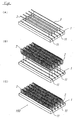
- FIG 1 through FIG 6 illustrate the first embodiment of the best mode for practicing the method for manufacturing the heat sink according to the invention.
- the heat sink in the first embodiment comprises a radiating substrate 1 and radiating fins 2, which are united by soldering.
- the radiating substrate 1 is formed of a flat plate having high thermal conductivity To be more specific, it may be made from metallic material such as aluminum, copper, silver and gold or carbon material. As the metallic material, there may be used an alloy of such a metallic material and nickel, magnesium, zinc or silicon. As the occasion demands, it may be subjected to surface treatment with a material having no significant adverse effect on soldering to increase heat conductivity and corrosion resistivity. There are formed slit-like insertion grooves 11 in one surface of the radiating substrate 1 (opposite surface of a mounting surface to be attached to a semiconductor device). The insertion groove 11 may be formed by cutting, die-casting, or extrusion-molding.
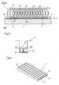
- the radiating fin 2 is formed by winding the same metal wire as the radiating substrate 1 into a coil and flattened so as to bring flattened loops of the coiled radiating fin of metal wire into close contact with one another.
- the radiating fins 2 may be typically assembled by interdigitating the loops of the opposed radiating fin coils 21 and 22 having the same size and wound in the opposite direction at the same pitch and then compressing the coils 21 and 22 one on top of the other to be united into one body.
- the coils are compressed in such a manner that the center parts 211 and 221 of the coils 21 and 22 are bent inwardly (toward the inner side of the overlaid coils) and then the front side parts of the overlaid coils 21 and 22 are crushed to form flat surfaces 212 and 222.
- the coils 12 and 22 of the radiating fins thus formed have the outwardly-projecting center portions 211 and 221 bent inwardly to reduce the thickness by S, consequently to form the complex uneven surface having the side edge portions 213 and 223 of the tangled metal wires.
- the material of the radiating fin 2 various kinds of materials similarly to the aforementioned radiating substrate 1 may be used.
- metallic material such as aluminum, copper, silver and gold or an alloy of such a metallic material and nickel, magnesium, zinc or silicon.
- affordable aluminum materials having high thermal conductivity are good for the radiating fin.
- An anticorrosion metal may be used as the metal wire of the radiating fin 2. Since the heat sink may be used in a corrosion-prone environment depending on its usage, the radiating fin of anticorrosion metal is adequate in such an environment.
- the anticorrosion metal titan, titanium alloy and stainless steel may be included.
- the metal wire for the radiating fin 2 may be subjected to surface treatment for increasing heat conductivity and corrosion resistivity according to need.
- the surface treatment such as copper plating and silver plating is suitable.
- a commonly known surface treatment may be applied to the method for manufacturing the heat sink, e.g.
- an electrolytic method for forming a plating layer on a processing object used as a positive electrode in an electrolyte solution such as of oxalic acid, sulfuric acid and phosphoric acid As the anodic oxide coating treatment, there are a white alumite treatment and a black alumite treatment, which both are applicable to this invention.
- a coating including ferrite may be formed according to need.
- the ferrite of the coating has an effect of absorbing electromagnetic wave, consequently to provide an electromagnetic wave absorbing capacity to the heat sink 100 thus treated.
- the radiating fin 2 of the metal wire has the uneven surface inherently reflecting diffusely the electromagnetic wave, thus to synergistically increase the electromagnetic wave absorbing capacity.
- the ferrite there are soft magnetic ferrite (soft ferrite) and hard magnetic ferrite (hard ferrite), either, or a combination of both, of which may be used in the invention.
- a binder for dispersing the ferrite a common material such as acrylic resin or silicone resin can be used.
- a heat dissipation coating having heat dissipation properties may be formed for radiating heat generated in the radiating fin 2 where necessary.
- the aforementioned coating can be made of material containing various pigments having a thermal radiation effect.
- pigment there can be enumerated carbon black, alumina, zirconia, titania, silica, zircon, magnesia, yttria (Y 2 O 3 ), cordierite (2MgO ⁇ 2Al 2 O 3 ⁇ 5SiO 2 ), and aluminum titanate (Al 2 O 3 ⁇ TiO 2 ).
- carbon black alumina, zirconia, titania, silica, zircon, magnesia, yttria (Y 2 O 3 ), cordierite (2MgO ⁇ 2Al 2 O 3 ⁇ 5SiO 2 ), and aluminum titanate (Al 2 O 3 ⁇ TiO 2 ).
- the amount of the pigment contained in the coating is arbitrarily determined according to the required heat dissipation capacity, and in general, should be suitably at a rate of 10 to 90 percent by mass of the coating in its dry condition.
- a material hard to deteriorate with heat is suitable for the binder, e.g. acrylate resin, silicone resin, urethane resin, polyester resin and fluorocarbon polymer. It is appropriate to determine the thickness of the heat dissipation coating to 1 to 50 ⁇ m. The coating of less than 1 ⁇ m in thickness is not recommendable because it has a thermal radiation effect.
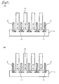
- solder strip 3 is put into each of the insertion grooves 11 formed in the radiating substrate 1 as shown in FIG 1(A), and then, the radiating fins 2 are respectively fitted into each insertion groove 11 stuffed with the solder strip 3 as shown in FIG 1 (B). Subsequently, the solder strip 3 is molten with a suitable heater in the state of holding the radiating fins 2 on the radiating substrate 1 as shown in FIG 1(C).
- soldering When soldering, the solder 3 in the state molten by heat is prevented from flowing out by the insertion grooves 11 in the radiating substrate 1, as the result of which the molten solder infiltrates toward the center parts 211 and 221 of the radiating substrate from the side edge portions 213 and 223 of the radiating fin having the complex uneven surface by capillary action. Therefore, soldering deposit resulting from the molten solder 3 is widely spread in a strip form over the punctate contact portions between the flat surface of the radiating substrate 1 and the curved parts of the radiating fins 2, consequently to increase the strength of the union between the radiating substrate 1 and radiating fins 2 and improve the heat conductivity between the radiating substrate 1 and the radiating fins 2.
- the amount of the solder 3 should be determined to bring the coils 21 and 22 into steady contact with the molten solder 3 as shown in FIG 5.
- the first embodiment of the heat sink made by soldering makes it possible to secure densely the radiating substrate 1 and radiating fins 2 and significantly improve the heat conductivity between the radiating substrate 1 and the radiating fins 2 due to the small thickness S of the radiating fin 2.
- the depth d of each insertion groove 11 so as to bring parts of the flat surfaces 212 and 222 of the coils 21 and 22 of the radiating fins 2 into contact with the side walls of the insertion grooves 11 in the radiating substrate 1, the contact area between the radiating substrate 1 and the radiating fins 2 can be enlarged consequently to further improve the heat conductivity between the radiating substrate 1 and the radiating fins 2.
- FIG 6 shows the modified example of the radiating substrate 1 in the aforementioned first embodiment.
- the radiating substrate 1 in this embodiment has the insertion grooves 11 formed by arranging spacer plates 12 such as of metallic material having high thermal conductivity at intervals on the radiating substrate.
- This embodiment having the insertion grooves is effective for the radiating substrate 1 formed of a material hard to process.
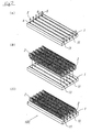
- FIG 7 shows the second embodiment of the best mode for practicing the method for manufacturing the heat sink 100 according to the invention.
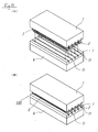
- the radiating substrate 1 and radiating fins 2 are secured with thermally-conductive adhesive 4.
- the radiating substrate 1 and radiating fins 2 are the same as those in the first embodiment.
- the thermally-conductive adhesive 4 is made by mixing metal powder such as of gold, silver, nickel or the like and/or power of alumina, alumina nitride, silicon nitride, carbon or the like with a binder such as of epoxy resin, silicon resin, acrylate resin, urethane resin or the like.
- the thermally-conductive adhesive 4 may be sprayed intensively onto the insertion grooves 11 in the radiating substrate 1 by using a nozzle 5 as shown in FIG 7(A).
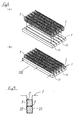
- FIG 8 and FIG. 9 show the third and fourth embodiments of the best mode for practicing the method for manufacturing the heat sink 100 according to the invention.
- the radiating substrate 1 and radiating fins 2 are secured by deforming the insertion grooves 11 in the radiating substrate 1.
- the radiating substrate 1 and radiating fins 2 in the third and fourth embodiments are the same as that in the first embodiment.
- the insertion groove 11 in the radiating substrate 1 is deformed by calking under pressure in the width direction to unite the radiating fins 2 to the radiating substrate 1.
- the side edge portions 213 and 223 having the complex uneven surfaces of the coils 21 and 22 of the radiating fins 2 fitted into the insertion grooves 11 are more intricately deformed as the insertion grooves 11 in the radiating substrate 1 are deformed
- the punctate contact portions between the flat surface of the radiating substrate 1 and the curved portions of the radiating fins 2 are significantly enlarged consequently to increase the strength of the union between the radiating substrate 1 and radiating fins 2 and improve the heat conductivity between the radiating substrate 1 and the radiating fins 2.
- the parts in the vicinity of the insertion grooves 11 in the radiating substrate 1 are deformed under vibrational pressure imparted by a vibration pressure plate 8.
- the insertion grooves 11 are deformed under vibrational pressure imparted by the vibration pressure plate 8 to bring the radiating fins 2 into press contact with the radiating substrate 1.
- High frequency vibration enables prompt uniting of the radiating substrate 1 and radiating fins 2.
- the side edge portions 213 and 223 having the complex uneven surfaces of the coils 21 and 22 of the radiating fins 2 fitted into the insertion grooves 11 are more intricately deformed as the insertion grooves 11 in the radiating substrate 1 are deformed.
- the punctate contact portions between the flat surface of the radiating substrate 1 and the curved portions of the radiating fins 2 are significantly enlarged consequently to increase the strength of the union between the radiating substrate 1 and radiating fins 2 and improve the heat conductivity between the radiating substrate 1 and the radiating fins 2.
- the deforming of the insertion grooves 11 in the radiating substrate 1 can be fulfilled by calking under pressure imparted on the radiating substrate 1 in the width direction of the insertion grooves 11 as in the third embodiment, or by the vibrational pressure imparted the portions in the vicinity of the insertion grooves 11 in the radiating substrate 1 as in the fourth embodiment, there may be alternatively employed heat treatment in which while widening the insertion grooves 11 in the radiating substrate 1 due to thermal expansion on heating, the radiating fins 2 are inserted into the insertion grooves, and thereafter, the entire is cooled to deflate the insertion grooves.
- FIG 11 shows the fifth embodiment of the best mode for practicing the method for manufacturing the heat sink 100 according to the invention.
- the radiating substrate 1 and radiating fins are secured by welding.
- the radiating substrate 1 and radiating fins are the same as those in the first embodiment.
- the radiating fins 2 are fitted into the insertion grooves in the radiating substrate 1 fixed on a holder base 6 while being held by a support frame 7 having slits corresponding to the insertion grooves 11 of the radiating substrate 1 and united with the radiating substrate by welding.
- flash welding or vibrational welding may be adopted.
- vibration welding in the state that the radiating fins 2 integrally held by the support frame 7 are inserted into the insertion grooves 11 in the radiating substrate 1, the contact portions are subjected to solid-state welding due to friction caused by pressure and powerful ultrasonic vibration imparted to the radiating fins 2.
- the vibration can be uniformly transmitted to the entire radiating fins 2 held by the support frame 7.
- the molten materials brought about by welding the radiating substrate 1 and radiation fins 2 have the same function and effect as the solder 3 in the first embodiment.
- the radiating fins 2 may be secured on the radiating substrate 1 by using a jig or other possible tools without forming the insertion grooves 11 in the radiating substrate 1.
- the radiating fin 2 in the aforementioned embodiment is made of the entirely flattened metal wire wound in a coil, the invention should not be understood as being limited thereto.
- the metal wire applied for the radiating fin may be flattened in part. For instance, only the side edge portions of the radiating fin to be in contact with the radiating substrate may be made flat, so that the side edge portions in contact with the radiating substrate have complex uneven surface of the densely coiled metal wire while assuming coarsely coiled metal wire at the other portions than the side edge portions at the central part of the radiating substrate to substantially expand the heat dissipation space.
- the heat generated in the radiating substrate is transmitted to the entire radiating fins through the side edge portions of the densely coiled metal wire.
- the heat spread throughout the radiating fins is promptly released from the heat dissipation space defined in the central part of the coarsely coiled metal wire.
- the coiled metal wire is partially flattened, the forming cost can be reduced.
Landscapes
- Engineering & Computer Science (AREA)
- Theoretical Computer Science (AREA)
- Human Computer Interaction (AREA)
- Physics & Mathematics (AREA)
- General Engineering & Computer Science (AREA)
- General Physics & Mathematics (AREA)
- Cooling Or The Like Of Semiconductors Or Solid State Devices (AREA)
- Cooling Or The Like Of Electrical Apparatus (AREA)
Applications Claiming Priority (2)
| Application Number | Priority Date | Filing Date | Title |
|---|---|---|---|
| JP2004104919 | 2004-03-31 | ||
| PCT/JP2005/006309 WO2005096376A1 (fr) | 2004-03-31 | 2005-03-31 | Procédé de fabrication de dissipateur thermique |
Publications (2)
| Publication Number | Publication Date |
|---|---|
| EP1737035A1 true EP1737035A1 (fr) | 2006-12-27 |
| EP1737035A4 EP1737035A4 (fr) | 2010-01-20 |
Family
ID=35064076
Family Applications (1)
| Application Number | Title | Priority Date | Filing Date |
|---|---|---|---|
| EP05727986A Withdrawn EP1737035A4 (fr) | 2004-03-31 | 2005-03-31 | Procédé de fabrication de dissipateur thermique |
Country Status (6)
| Country | Link |
|---|---|
| US (1) | US20070223195A1 (fr) |
| EP (1) | EP1737035A4 (fr) |
| JP (1) | JP4601610B2 (fr) |
| KR (1) | KR100978917B1 (fr) |
| CN (1) | CN1938847B (fr) |
| WO (1) | WO2005096376A1 (fr) |
Cited By (3)
| Publication number | Priority date | Publication date | Assignee | Title |
|---|---|---|---|---|
| US20110012494A1 (en) * | 2007-07-05 | 2011-01-20 | Fawoo Technology Co., Ltd. | Heat dissipating device having linear heat dissipating unit and fanless led lamp using the device |
| EP2201284A4 (fr) * | 2007-10-26 | 2011-06-15 | Fawoo Technology Co Ltd | Lampe à éclairage par diode électroluminescente |
| EP3293453A1 (fr) * | 2016-09-09 | 2018-03-14 | Valeo Iluminacion | Dispositif d'eclairage comprenant un element de dissipation de chaleur |
Families Citing this family (13)
| Publication number | Priority date | Publication date | Assignee | Title |
|---|---|---|---|---|
| TWI381494B (zh) * | 2004-01-07 | 2013-01-01 | 事業創造研究所股份有限公司 | Cooling device |
| JP4969973B2 (ja) * | 2005-11-16 | 2012-07-04 | 臼井国際産業株式会社 | ヒートシンク |
| JP2008098591A (ja) * | 2006-10-16 | 2008-04-24 | Jigyo Sozo Kenkyusho:Kk | ヒートシンク及びその製造方法 |
| JP2009188032A (ja) * | 2008-02-04 | 2009-08-20 | Fuji Electric Systems Co Ltd | 電力変換装置 |
| KR101186781B1 (ko) * | 2008-06-12 | 2012-09-27 | 미쓰비시덴키 가부시키가이샤 | 전력 반도체 회로 장치 및 그 제조 방법 |
| KR100904391B1 (ko) * | 2008-06-30 | 2009-06-26 | 박교양 | 방열 조명 램프 |
| US20100123848A1 (en) * | 2008-11-18 | 2010-05-20 | Samsung Electronics Co., Ltd. | Led module and liquid crystal display having the same |
| EP3113590B1 (fr) * | 2015-06-30 | 2020-11-18 | ABB Schweiz AG | Appareil de refroidissement |
| KR102433388B1 (ko) * | 2015-10-22 | 2022-08-17 | 삼성전자주식회사 | 공기 조화기의 실외기, 이에 적용되는 냉각 유닛 및 냉각 유닛의 제조 방법 |
| CN106455443A (zh) * | 2016-11-03 | 2017-02-22 | 常州热盛换热器有限公司 | 一种散热器及基于该散热器的成型工艺 |
| CN107717357A (zh) * | 2017-11-14 | 2018-02-23 | 北京动力机械研究所 | 一种异型曲面夹层结构金属壳体的制造方法 |
| US10651109B2 (en) * | 2018-07-16 | 2020-05-12 | Infineon Technologies Ag | Selective plating of semiconductor package leads |
| TWI813277B (zh) * | 2022-05-06 | 2023-08-21 | 邁萪科技股份有限公司 | 改良除氣管固定結構的均溫板 |
Family Cites Families (21)
| Publication number | Priority date | Publication date | Assignee | Title |
|---|---|---|---|---|
| BE561245A (fr) * | ||||
| US1516430A (en) * | 1921-08-25 | 1924-11-18 | Christopher A Hess | Water heater |
| US1960305A (en) * | 1933-08-10 | 1934-05-29 | Gen Motors Corp | Radiator spiral coil tube |
| US2277462A (en) * | 1939-12-22 | 1942-03-24 | Gen Electric | Heat transfer surface |
| US2595457A (en) * | 1947-06-03 | 1952-05-06 | Air Preheater | Pin fin heat exchanger |
| US2784947A (en) * | 1954-09-13 | 1957-03-12 | Air Preheater | Heat exchange assembly |
| GB768464A (en) * | 1954-10-25 | 1957-02-20 | Gallay Ltd | Improvements in or relating to heat exchanger elements |
| DE1165621B (de) * | 1957-10-23 | 1964-03-19 | Helmut Alfred Freyholdt | Waermeaustauscherelement mit drahtfoermigen Elementen in den Kanaelen und aus aufeinandergeschichteten Streifen bestehenden Trennwaenden |
| GB1056104A (en) * | 1962-07-20 | 1967-01-25 | Oestbo John D B | Improvements in or relating to heat-exchangers, pre-heaters and economizers |
| US3543844A (en) * | 1968-05-17 | 1970-12-01 | Air Reduction | Multiple-pass heat exchanger for cryogenic systems |
| GB2146423A (en) * | 1984-09-07 | 1985-04-17 | Redpoint Limited | Heat transfer devices |
| US4955523A (en) * | 1986-12-17 | 1990-09-11 | Raychem Corporation | Interconnection of electronic components |
| JPH0381640U (fr) * | 1989-12-07 | 1991-08-21 | ||
| JPH0471257A (ja) * | 1990-07-11 | 1992-03-05 | Hitachi Ltd | 電子装置 |
| JPH04243153A (ja) * | 1991-01-16 | 1992-08-31 | Akutoronikusu Kk | ヒートシンクとその製造方法 |
| JP2873765B2 (ja) * | 1992-04-13 | 1999-03-24 | アクトロニクス 株式会社 | ▲l▼字形状ピン群を有する剣山型ヒートシンク |
| JPH06275746A (ja) * | 1993-03-18 | 1994-09-30 | Hitachi Ltd | 半導体装置 |
| JPH07297327A (ja) * | 1994-04-27 | 1995-11-10 | Toshiba Corp | 半導体装置およびその製造方法 |
| JPH1154676A (ja) * | 1997-08-07 | 1999-02-26 | Ebara Densen Kk | 放熱部品 |
| JP2002190557A (ja) * | 2000-12-21 | 2002-07-05 | Fujikura Ltd | ワイヤーヒートシンク |
| US20020079097A1 (en) * | 2000-12-21 | 2002-06-27 | Seri Lee | Heat sink |
-
2005
- 2005-03-31 WO PCT/JP2005/006309 patent/WO2005096376A1/fr not_active Ceased
- 2005-03-31 CN CN2005800101726A patent/CN1938847B/zh not_active Expired - Fee Related
- 2005-03-31 EP EP05727986A patent/EP1737035A4/fr not_active Withdrawn
- 2005-03-31 KR KR1020067018465A patent/KR100978917B1/ko not_active Expired - Fee Related
- 2005-03-31 JP JP2006511805A patent/JP4601610B2/ja not_active Expired - Fee Related
- 2005-03-31 US US10/594,505 patent/US20070223195A1/en not_active Abandoned
Cited By (3)
| Publication number | Priority date | Publication date | Assignee | Title |
|---|---|---|---|---|
| US20110012494A1 (en) * | 2007-07-05 | 2011-01-20 | Fawoo Technology Co., Ltd. | Heat dissipating device having linear heat dissipating unit and fanless led lamp using the device |
| EP2201284A4 (fr) * | 2007-10-26 | 2011-06-15 | Fawoo Technology Co Ltd | Lampe à éclairage par diode électroluminescente |
| EP3293453A1 (fr) * | 2016-09-09 | 2018-03-14 | Valeo Iluminacion | Dispositif d'eclairage comprenant un element de dissipation de chaleur |
Also Published As
| Publication number | Publication date |
|---|---|
| KR20070007312A (ko) | 2007-01-15 |
| US20070223195A1 (en) | 2007-09-27 |
| WO2005096376A1 (fr) | 2005-10-13 |
| CN1938847A (zh) | 2007-03-28 |
| EP1737035A4 (fr) | 2010-01-20 |
| CN1938847B (zh) | 2010-10-27 |
| KR100978917B1 (ko) | 2010-08-31 |
| JP4601610B2 (ja) | 2010-12-22 |
| JPWO2005096376A1 (ja) | 2008-02-21 |
Similar Documents
| Publication | Publication Date | Title |
|---|---|---|
| EP1737035A1 (fr) | Procédé de fabrication de dissipateur thermique | |
| CN110313064B (zh) | 陶瓷金属电路基板及使用了该陶瓷金属电路基板的半导体装置 | |
| JP2001057405A (ja) | 放熱フィンを備えたヒートシンクおよび放熱フィンの固定方法 | |
| JP2002299529A (ja) | Ic放熱構造 | |
| JP2004311718A (ja) | ヒートシンク | |
| JP2020061482A (ja) | 放熱構造 | |
| JP2004158814A (ja) | 発熱体の放熱実装構造 | |
| JP3669980B2 (ja) | モジュール構造体の製造方法並びに回路基板の固定方法及び回路基板 | |
| JP4601667B2 (ja) | ヒートシンクおよびその製造方法 | |
| US7468554B2 (en) | Heat sink board and manufacturing method thereof | |
| JP4091896B2 (ja) | 半導体装置の製造方法 | |
| JP3602806B2 (ja) | コルゲートフィン型ヒートシンクの製造方法 | |
| JPH10313081A (ja) | 半導体装置およびその製造方法 | |
| CN112368533B (zh) | 热管结构体及热管结构体用压接夹具 | |
| JP3669981B2 (ja) | モジュール構造体の製造方法 | |
| CN217608155U (zh) | 一种散热基板、散热结构及散热器 | |
| JP2007165486A (ja) | 放熱板及び半導体装置 | |
| CN223207404U (zh) | 一种散热贴片的散热结构 | |
| JPH11233979A (ja) | 電子機器の放熱構造とこの放熱構造を用いた電源装置 | |
| JP2002120033A (ja) | 圧着式ヒートシンクの製造方法 | |
| JP5167543B2 (ja) | 放熱板付きリードフレームおよびその製造方法 | |
| WO2020087389A1 (fr) | Radiateur, carte de circuit imprimé et dispositif informatique | |
| JP2001162341A (ja) | フィン放熱器およびその製造方法 | |
| CN201018738Y (zh) | 散热模块的支架机构 | |
| JPH10310893A (ja) | 放熱体 |
Legal Events
| Date | Code | Title | Description |
|---|---|---|---|
| PUAI | Public reference made under article 153(3) epc to a published international application that has entered the european phase |
Free format text: ORIGINAL CODE: 0009012 |
|
| 17P | Request for examination filed |
Effective date: 20060928 |
|
| AK | Designated contracting states |
Kind code of ref document: A1 Designated state(s): AT BE BG CH CY CZ DE DK EE ES FI FR GB GR HU IE IS IT LI LT LU MC NL PL PT RO SE SI SK TR |
|
| DAX | Request for extension of the european patent (deleted) | ||
| A4 | Supplementary search report drawn up and despatched |
Effective date: 20091217 |
|
| STAA | Information on the status of an ep patent application or granted ep patent |
Free format text: STATUS: THE APPLICATION IS DEEMED TO BE WITHDRAWN |
|
| 18D | Application deemed to be withdrawn |
Effective date: 20100316 |