EP1737042A1 - Spannungsgesteuerte halbleitereinrichtung - Google Patents
Spannungsgesteuerte halbleitereinrichtung Download PDFInfo
- Publication number
- EP1737042A1 EP1737042A1 EP05721021A EP05721021A EP1737042A1 EP 1737042 A1 EP1737042 A1 EP 1737042A1 EP 05721021 A EP05721021 A EP 05721021A EP 05721021 A EP05721021 A EP 05721021A EP 1737042 A1 EP1737042 A1 EP 1737042A1
- Authority
- EP
- European Patent Office
- Prior art keywords
- semiconductor
- layer
- region
- voltage
- semiconductor layer
- Prior art date
- Legal status (The legal status is an assumption and is not a legal conclusion. Google has not performed a legal analysis and makes no representation as to the accuracy of the status listed.)
- Withdrawn
Links
Images



Classifications
-
- H—ELECTRICITY
- H10—SEMICONDUCTOR DEVICES; ELECTRIC SOLID-STATE DEVICES NOT OTHERWISE PROVIDED FOR
- H10D—INORGANIC ELECTRIC SEMICONDUCTOR DEVICES
- H10D62/00—Semiconductor bodies, or regions thereof, of devices having potential barriers
- H10D62/10—Shapes, relative sizes or dispositions of the regions of the semiconductor bodies; Shapes of the semiconductor bodies
- H10D62/17—Semiconductor regions connected to electrodes not carrying current to be rectified, amplified or switched, e.g. channel regions
- H10D62/393—Body regions of DMOS transistors or IGBTs
-
- H—ELECTRICITY
- H10—SEMICONDUCTOR DEVICES; ELECTRIC SOLID-STATE DEVICES NOT OTHERWISE PROVIDED FOR
- H10D—INORGANIC ELECTRIC SEMICONDUCTOR DEVICES
- H10D12/00—Bipolar devices controlled by the field effect, e.g. insulated-gate bipolar transistors [IGBT]
- H10D12/211—Gated diodes
-
- H—ELECTRICITY
- H10—SEMICONDUCTOR DEVICES; ELECTRIC SOLID-STATE DEVICES NOT OTHERWISE PROVIDED FOR
- H10D—INORGANIC ELECTRIC SEMICONDUCTOR DEVICES
- H10D12/00—Bipolar devices controlled by the field effect, e.g. insulated-gate bipolar transistors [IGBT]
- H10D12/411—Insulated-gate bipolar transistors [IGBT]
- H10D12/441—Vertical IGBTs
-
- H—ELECTRICITY
- H10—SEMICONDUCTOR DEVICES; ELECTRIC SOLID-STATE DEVICES NOT OTHERWISE PROVIDED FOR
- H10D—INORGANIC ELECTRIC SEMICONDUCTOR DEVICES
- H10D18/00—Thyristors
- H10D18/40—Thyristors with turn-on by field effect
-
- H—ELECTRICITY
- H10—SEMICONDUCTOR DEVICES; ELECTRIC SOLID-STATE DEVICES NOT OTHERWISE PROVIDED FOR
- H10D—INORGANIC ELECTRIC SEMICONDUCTOR DEVICES
- H10D18/00—Thyristors
- H10D18/60—Gate-turn-off devices
- H10D18/65—Gate-turn-off devices with turn-off by field effect
- H10D18/655—Gate-turn-off devices with turn-off by field effect produced by insulated gate structures
-
- H—ELECTRICITY
- H10—SEMICONDUCTOR DEVICES; ELECTRIC SOLID-STATE DEVICES NOT OTHERWISE PROVIDED FOR
- H10D—INORGANIC ELECTRIC SEMICONDUCTOR DEVICES
- H10D62/00—Semiconductor bodies, or regions thereof, of devices having potential barriers
- H10D62/10—Shapes, relative sizes or dispositions of the regions of the semiconductor bodies; Shapes of the semiconductor bodies
- H10D62/102—Constructional design considerations for preventing surface leakage or controlling electric field concentration
- H10D62/103—Constructional design considerations for preventing surface leakage or controlling electric field concentration for increasing or controlling the breakdown voltage of reverse-biased devices
- H10D62/105—Constructional design considerations for preventing surface leakage or controlling electric field concentration for increasing or controlling the breakdown voltage of reverse-biased devices by having particular doping profiles, shapes or arrangements of PN junctions; by having supplementary regions, e.g. junction termination extension [JTE]
- H10D62/106—Constructional design considerations for preventing surface leakage or controlling electric field concentration for increasing or controlling the breakdown voltage of reverse-biased devices by having particular doping profiles, shapes or arrangements of PN junctions; by having supplementary regions, e.g. junction termination extension [JTE] having supplementary regions doped oppositely to or in rectifying contact with regions of the semiconductor bodies, e.g. guard rings with PN or Schottky junctions
- H10D62/107—Buried supplementary regions, e.g. buried guard rings
Definitions
- the present invention relates to a power semiconductor for controlling large current, and more particularly relates to a voltage-controlled semiconductor device such as insulated-gate bipolar transistors having high breakdown voltage.
- Si silicon carbide
- IGBT insulated-gate bipolar transistor
- the inversion layer has low channel mobility. This is considered to be because a surface state is present in the interface between SiO 2 used as the gate insulating film and SiC so that the holes flowing through the inversion layer at on time are captured by the surface state. Further, it is also considered that roughness of the interface causes the holes as carriers to stop contributing to the conductivity, which causes the low mobility of the holes in the channel. Because of these reasons, channel resistance and on-voltage tend to increase.
- a voltage-controlled semiconductor device comprising:
- an embedded semiconductor region is provided in the vicinity of the surface of the second semiconductor layer which is in contact with the channel layer, the channel layer facing the control electrode via the insulating film. Consequently, without application of a voltage to between the control electrode and the second electrode at off time, current can be blocked by a built-in voltage of the Sic semiconductor. That is, the normally-off characteristic, i.e., capability of maintaining the off-state, can be implemented.
- holes are flowed from the channel layer into the second semiconductor layer so that a base current is fed to an npn transistor composed of the embedded semiconductor region, the second semiconductor layer and the first semiconductor layer, while a main current is flowed from the semiconductor region into the first semiconductor layer.
- conductivity modulation occurs in the base layer or the channel layer so that the resistance in the second semiconductor layer can be reduced considerably. This can lead to considerable reduction of the on-voltage.
- At least another first conductivity-type electric field relaxation layer is provided onto the second conductivity-type second semiconductor layer placed between the first conductivity-type embedded semiconductor regions.
- This allows considerable reduction of maximum electric fields applied to the insulating film at off time.
- a control electrode facing the second semiconductor layer via the insulating film is provided on the second conductivity-type second semiconductor layer placed between the first conductivity-type embedded semiconductor regions. This makes it possible to increase inflow of holes to the second semiconductor layer. The inflow of the holes to the second semiconductor layer leads to the increase of current passing through the second semiconductor layer, which allows further reduction of the on-voltage.
- the voltage-controlled semiconductor device of the present invention has a channel layer which faces a gate electrode via a gate insulating film and a base layer in contact with the channel layer, the base layer being partially provided with a plurality of embedded collector regions. At on time, holes are accumulated in the channel layer in the vicinity of the gate insulating film, resulting in formation of a low-resistant channel, through which a large base current is fed to a transistor composed of the embedded collector region, the base layer and the emitter layer. This causes conductivity modulation inside the base layer. As a result, a voltage-controlled semiconductor device having low on-resistance, i.e., low on-voltage, can be provided.
- a buffer layer 2 made of a p-type SiC semiconductor with a thickness of approx. 3 ⁇ m and a dopant concentration of approx. 1 ⁇ 10 17 cm -3 is formed on an emitter layer 1 (first semiconductor layer) as a substrate made of an n-type 4H-SiC semiconductor with a thickness of approx. 300 ⁇ m and with a high dopant concentration, the emitter layer 1 having an emitter electrode 7 (first electrode) made of gold, copper or the like on the lower surface thereof.
- the emitter electrode 7 is connected to an emitter terminal 7a.
- a base layer 3 (second semiconductor layer) made of a p-type SiC semiconductor with a thickness of approx.
- the base layer 3 Formed on both upper end portions of the base layer 3 is an embedded collector region 5 (embedded semiconductor region) made of n+type SiC semiconductor with a dopant concentration of 1 ⁇ 10 18 cm -3 to 1 ⁇ 10 19 cm -3 achieved by ion implantation and the like.
- an embedded collector region 5 embedded semiconductor region
- a channel layer 4 made of a p-type SiC semiconductor with a dopant concentration of 1 ⁇ 10 14 cm -3 to 3 ⁇ 10 16 cm -3 .
- the thickness of the channel layer 4 is approx. 0.2 ⁇ m to 2 ⁇ m. The thickness, which is determined by depending on the dopant concentration of the channel layer 4, may be smaller or larger than the above value in some cases.
- the dopant concentration of the channel layer 4 is larger than the dopant concentration of the base layer 3.
- the dopant concentration of the channel layer 4 may be smaller than the dopant concentration of the base layer 3.
- the dopant concentration of the channel layer 4 may also be equal to the dopant concentration of the base layer 3, and in such a case, by forming the embedded collector region 5 inside the base layer 3 by ion implantation, the base layer 3 and the channel layer 4 can be formed in the same step.
- a collector region 6 semiconductor region made of a p+type SiC semiconductor with a dopant concentration of approx. 1x10 19 cm -3 .
- the collector region 6 is shorter in the transverse direction than the embedded collector region 5.
- a gate insulating film 10 (insulating film) is formed on both the collector regions 6 and the channel layer 4, and a gate electrode 9 (control electrode) connected to a gate terminal 9a is provided on the gate insulating film 10.
- a collector electrode 8 (second electrode) connected to a collector terminal 8a is provided so as to be in contact with a lateral surface of the collector region 6 and with an upper surface of the embedded collector region 5.
- the collector electrode 8 and the gate electrode 9 are formed from metal films made of gold, copper or the like.
- the SiC-IGBT in the present embodiment when a voltage is applied to between the emitter electrode 7 and the collector electrode 8 so that the potential of the collector electrode 8 is high and then the potential of the gate electrode 9 is set to be lower than the potential of the collector electrode 8, the SiC-IGBT is turned on and a main current flows to between the collector electrode 8 and the emitter electrode 7.
- the voltage between the gate electrode 9 and the collector electrode 8 is set at 0, or the potential of the gate electrode 9 is set to be positive with respect to the collector electrode 8 in the state that the potential of the collector electrode 8 is higher than the potential of the emitter electrode 7.
- a depletion layer spreads in the channel layer 4 from a junction between the embedded collector region 5 and the channel layer 4, which brings the channel layer 4 in a pinch-off state. Consequently, the current flowing from the collector region 6 to the emitter layer 1 is blocked, as a result of which the SiC-IGBT is put in an off state, i.e., a normally-off state.
- the holes go into the base layer 3 from the collector region 6 through the channel and travels from the base layer 3 to the emitter layer 1. Electrons corresponding to the base current go into the base layer 3 from the emitter layer 1 and reach the embedded collector region 5. By widening an interval between the adjacent embedded collector regions 5, conductivity modulation is induced in the base layer 3 by the holes and the electrons coming into the base layer 3 from the embedded collector region 5, by which the resistance of the base layer 3 is considerably reduced.
- an "accumulation-type” operation is performed in which holes are accumulated in the channel layer 4.
- channel resistance is smaller than that in the "inversion-type” operation described in the BACKGROUND ART.
- the main current flows through an inversion-type channel on the lateral wall of the gate insulating film, and this causes large voltage drop in the channel portion.
- the SiC-IGBT in the present embodiment the main current does not flow through the channel layer 4 but only a gate current flows therethrough, so that the voltage drop in the channel layer 4 can be kept small.
- the embedded collector region 5 has high dopant concentration and small resistance, the voltage drop in this region is small.
- the on-voltage was 3.5 V, which was considerably lower than 9.5 V, the on-voltage of the conventional SiC-IGBT.
- an interval between the adjacent embedded collector regions 5 was 3 ⁇ m or more, increasing the interval to 10 ⁇ m decreased the resistance between the embedded collector regions 5. Consequently, the base current flowing from the collector region 6 through the channel layer 4 became larger, and this increased the main current. As a result, the on-voltage was further decreased to 3.2 V.
- the embedded collector region 5 is formed by ion implantation in the present embodiment
- an embedded collector region similar to the embedded collector region 5 in the present embodiment can be formed by the steps of forming an n+ region through epitaxial method and etching away the region except a necessary portion.
- the channel layer 4 on the embedded collector region 5 has sufficient crystallinity and high channel mobility compared to the channel layer 4 in the case of ion implantation.
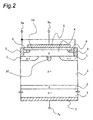
- Fig. 2 is a cross sectional view showing a segment of a voltage-controlled semiconductor device in a second embodiment of the present invention, i.e., an insulated-gate bipolar transistor (SiC-IGBT) with use of a SiC semiconductor and with a breakdown voltage of 10 kV.
- SiC-IGBT insulated-gate bipolar transistor
- the SiC-IGBT in the present embodiment is different from the first embodiment in the point that at least one electric field relaxation region 55 made of an n+ SiC semiconductor is provided in the base layer 3 between the adjacent embedded collector regions 5.
- Other structural features are similar to those of the first embodiment.
- the dopant concentration of the electric field relaxation region 55 may be identical to that of the embedded collector region 5.
- the electric field relaxation region 55 and the embedded collector region 5 can be manufactured in the same step, so that simplification of the steps can be achieved.
- a depletion layer spreads in the base layer 3 from a junction between the electric field relaxation region 55 and the base layer 3 at off time of the SiC-IGBT, and therefore a collector-emitter voltage can be shared. As a result, it becomes possible to relax the electric field intensity applied to the gate insulating film 10.
- a central portion 10g of the gate insulating film 10a facing the base layer 3 between the adjacent embedded collector regions 5 was higher in electric field intensity than other portions of the gate insulating film 10a at off time.
- the reason thereof is considered to be as follows.
- an accumulation layer is formed in the range from the upper side of the embedded collector regions 5 up to as close as to a central region on an interval between the adjacent embedded collector regions 5. This decreases voltage drop during the passage of the base current. Further, the interval between the adjacent embedded collector regions 5 is widened so that conductivity modulation sufficiently occurs in the base layer 3.
- the depletion layer does not fully spread in the vicinity of the central region between the embedded collector regions 5 since the interval therebetween is wide. Consequently, the collector voltage is not shared by the depletion layer, by which the central portion 10g of the gate insulating film 10a has a high electric field. More specifically, at off time, the depletion layer spreading to the base layer 3 and the channel layer 4 from the junction between the embedded collector region 5 and the base layer 3 shares the voltage between the collector region 6 and the emitter layer 1.
- the depletion layer does not fully spread in the central portions of the base layer 3 and the channel layer 4 placed between the adjacent embedded collector regions 5, as a result of which high electric fields are easily applied to the central portion 10g of the gate insulating film 10a. Accordingly, the thickness of the central portion 10g of the gate insulating film 10a is made larger than that of other portions so as to enhance electric field intensity withstand characteristics. This makes it possible to reduce the maximum electric field intensity applied to the gate insulating film 10a at off time.
- the thickness of the central portion 10g in the gate insulating film 10a with a thickness of approx. 0.1 ⁇ m is set at approx. 0.5 ⁇ m, which is about five times larger than that of other portions. This makes it possible to reduce approx. 70% of the maximum electric field intensity applied to the central portion 10g of the gate insulating film 10a at off time.
- Fig. 4 is a cross sectional view showing a segment of a voltage-controlled semiconductor device in a fourth embodiment of the present invention, i.e., an insulated-gate bipolar transistor (SiC-IGBT) with use of a SiC semiconductor and with a breakdown voltage of 10 kV.
- the SiC-IGBT in the present embodiment has a trench 15 provided in the central portion of the SiC-IGBT, the trench 15 extending through a channel layer 4a and going into the base layer 3.
- An electric field relaxation layer 56 made of an n+ SiC semiconductor is provided on the bottom portion of the trench 15. Though the electric field relaxation layer 56 should preferably be narrower than the width of the trench 15, it is acceptable that the electric field relaxation layer 56 is wider than the width of the trench 15.
- a gate insulating film 10b is provided on the lateral wall of the trench 15 and on the electric field relaxation layer 56.
- a gate electrode 9 is provided inside the trench 15 via the gate insulating film 10b.
- the gate electrode 9 faces the upper surface of the channel layer 4a via the gate insulating film 10b while facing the lateral surface of the channel layer 4a inside the trench 15 via the gate insulating film 10b.
- Other structural features are identical to those in the first embodiment shown in Fig. 1.
- a SiC-IGBT in another example of the present embodiment shown in Fig. 5 does not have the electric field relaxation layer 56 in the SiC-IGBT shown in Fig. 4 for the purpose of simplifying the structure. Except the maximum electric field intensity being slightly lower than that of the SiC-IGBT shown in Fig. 4 due to the absence of the electric field relaxation layer 56, the SiC-IGBT in the present example operates in a manner similar to the SiC-IGBT shown in Fig. 4. The SiC-IGBT in the present example also shares the characteristic with the present embodiment, that is, the capability of increasing the base current and decreasing the on-voltage.
- the present invention is also applicable to the voltage-controlled semiconductor device with a structure in which n-type layers and regions are respectively replaced with p-type layers and regions while p-type layers and regions are respectively replaced with n-type layers and regions.
- forming the channel layer 4 as an accumulation-type layer allows the channel resistance to become smaller than that in the case of the inversion type layer.
- an effect of further reducing the resistance of the channel layer 4 can be implemented by forming a p-type high-conductivity region 4b with a high dopant concentration on the surface or inside the channel layer 4.
- the high-conductivity region 4b is formed in a depth of about 0.05 ⁇ m to 0.5 ⁇ m from the interface between the channel layer 4 and the gate insulating film 10 by epitaxial growth or by implantation of p-type ions such as aluminum ions into the channel layer 4.
- the depth and the thickness of the high-conductivity region 4b from the surface of the channel layer 4 are determined by depending on the dopant concentration, and therefore the thickness is decreased when the dopant concentration is high and the thickness is increased when the dopant concentration is low so that the channel resistance in the normally-off state can be reduced.
- One example of the dopant concentration and the thickness of the high-conductivity region 4b is about 3x10 16 cm -3 and 0.1 ⁇ m, respectively, when the thickness of the channel layer 4 is about 0.3 ⁇ m.
- Fig. 6 shows the high-conductivity region 4b added to the structure of Fig. 1, the similar effect can be achieved by adding the similar high-conductivity region to the channel layer in the voltage-controlled semiconductor devices in Fig. 2 to Fig. 5.
- the present invention is effectively applicable to devices with use of other wide gap semiconductor materials such as diamond and gallium nitride.
Landscapes
- Electrodes Of Semiconductors (AREA)
- Insulated Gate Type Field-Effect Transistor (AREA)
- Thin Film Transistor (AREA)
Applications Claiming Priority (2)
| Application Number | Priority Date | Filing Date | Title |
|---|---|---|---|
| JP2004083233A JP4237086B2 (ja) | 2004-03-22 | 2004-03-22 | 電圧制御型半導体装置 |
| PCT/JP2005/004834 WO2005091372A1 (ja) | 2004-03-22 | 2005-03-17 | 電圧制御型半導体装置 |
Publications (2)
| Publication Number | Publication Date |
|---|---|
| EP1737042A1 true EP1737042A1 (de) | 2006-12-27 |
| EP1737042A4 EP1737042A4 (de) | 2010-05-26 |
Family
ID=34993977
Family Applications (1)
| Application Number | Title | Priority Date | Filing Date |
|---|---|---|---|
| EP05721021A Withdrawn EP1737042A4 (de) | 2004-03-22 | 2005-03-17 | Spannungsgesteuerte halbleitereinrichtung |
Country Status (4)
| Country | Link |
|---|---|
| US (1) | US7626232B2 (de) |
| EP (1) | EP1737042A4 (de) |
| JP (1) | JP4237086B2 (de) |
| WO (1) | WO2005091372A1 (de) |
Cited By (4)
| Publication number | Priority date | Publication date | Assignee | Title |
|---|---|---|---|---|
| WO2014105372A1 (en) * | 2012-12-28 | 2014-07-03 | Cree, Inc. | Semiconductor devices having reduced electric field at a gate oxide layer |
| US10115815B2 (en) | 2012-12-28 | 2018-10-30 | Cree, Inc. | Transistor structures having a deep recessed P+ junction and methods for making same |
| US11417760B2 (en) | 2017-12-21 | 2022-08-16 | Wolfspeed, Inc. | Vertical semiconductor device with improved ruggedness |
| US11489069B2 (en) | 2017-12-21 | 2022-11-01 | Wolfspeed, Inc. | Vertical semiconductor device with improved ruggedness |
Families Citing this family (5)
| Publication number | Priority date | Publication date | Assignee | Title |
|---|---|---|---|---|
| DE102005040624A1 (de) * | 2004-09-02 | 2006-03-09 | Fuji Electric Holdings Co., Ltd., Kawasaki | Halbleiterbauteil und Verfahren zu seiner Herstellung |
| JP2009038200A (ja) * | 2007-08-01 | 2009-02-19 | Toyota Central R&D Labs Inc | 半導体装置 |
| JP2011060901A (ja) * | 2009-09-08 | 2011-03-24 | Sumitomo Electric Ind Ltd | 半導体装置および半導体装置の製造方法 |
| WO2011129443A1 (ja) | 2010-04-15 | 2011-10-20 | 富士電機株式会社 | 半導体装置 |
| WO2014021365A1 (ja) * | 2012-07-31 | 2014-02-06 | 独立行政法人産業技術総合研究所 | 半導体構造物、半導体装置及び該半導体構造物の製造方法 |
Family Cites Families (10)
| Publication number | Priority date | Publication date | Assignee | Title |
|---|---|---|---|---|
| DE19534154C2 (de) * | 1995-09-14 | 2001-06-28 | Siemens Ag | Durch Feldeffekt steuerbares Leistungs-Halbleiterbauelement |
| JPH1027899A (ja) | 1996-07-11 | 1998-01-27 | Fuji Electric Co Ltd | 電圧駆動型炭化ケイ素サイリスタ |
| JPH10256529A (ja) | 1997-03-14 | 1998-09-25 | Fuji Electric Co Ltd | 絶縁ゲート型炭化ケイ素サイリスタ |
| US5917204A (en) | 1997-03-31 | 1999-06-29 | Motorola, Inc. | Insulated gate bipolar transistor with reduced electric fields |
| US6342709B1 (en) * | 1997-12-10 | 2002-01-29 | The Kansai Electric Power Co., Inc. | Insulated gate semiconductor device |
| JP4541489B2 (ja) | 2000-04-06 | 2010-09-08 | 三菱電機株式会社 | 半導体装置及びその製造方法 |
| JP3916874B2 (ja) | 2001-02-06 | 2007-05-23 | 関西電力株式会社 | 半導体装置 |
| JP3800047B2 (ja) * | 2001-07-18 | 2006-07-19 | 日産自動車株式会社 | 電界効果トランジスタ |
| JP3559971B2 (ja) * | 2001-12-11 | 2004-09-02 | 日産自動車株式会社 | 炭化珪素半導体装置およびその製造方法 |
| US6940110B2 (en) * | 2002-11-29 | 2005-09-06 | Matsushita Electric Industrial Co., Ltd. | SiC-MISFET and method for fabricating the same |
-
2004
- 2004-03-22 JP JP2004083233A patent/JP4237086B2/ja not_active Expired - Fee Related
-
2005
- 2005-03-17 EP EP05721021A patent/EP1737042A4/de not_active Withdrawn
- 2005-03-17 WO PCT/JP2005/004834 patent/WO2005091372A1/ja not_active Ceased
- 2005-03-17 US US10/593,878 patent/US7626232B2/en not_active Expired - Fee Related
Cited By (8)
| Publication number | Priority date | Publication date | Assignee | Title |
|---|---|---|---|---|
| WO2014105372A1 (en) * | 2012-12-28 | 2014-07-03 | Cree, Inc. | Semiconductor devices having reduced electric field at a gate oxide layer |
| US9530844B2 (en) | 2012-12-28 | 2016-12-27 | Cree, Inc. | Transistor structures having reduced electrical field at the gate oxide and methods for making same |
| US10115815B2 (en) | 2012-12-28 | 2018-10-30 | Cree, Inc. | Transistor structures having a deep recessed P+ junction and methods for making same |
| US10840367B2 (en) | 2012-12-28 | 2020-11-17 | Cree, Inc. | Transistor structures having reduced electrical field at the gate oxide and methods for making same |
| US10886396B2 (en) | 2012-12-28 | 2021-01-05 | Cree, Inc. | Transistor structures having a deep recessed P+ junction and methods for making same |
| US11417760B2 (en) | 2017-12-21 | 2022-08-16 | Wolfspeed, Inc. | Vertical semiconductor device with improved ruggedness |
| US11489069B2 (en) | 2017-12-21 | 2022-11-01 | Wolfspeed, Inc. | Vertical semiconductor device with improved ruggedness |
| US12087854B2 (en) | 2017-12-21 | 2024-09-10 | Wolfspeed, Inc. | Vertical semiconductor device with improved ruggedness |
Also Published As
| Publication number | Publication date |
|---|---|
| US20070200150A1 (en) | 2007-08-30 |
| WO2005091372A1 (ja) | 2005-09-29 |
| US7626232B2 (en) | 2009-12-01 |
| JP4237086B2 (ja) | 2009-03-11 |
| JP2005268731A (ja) | 2005-09-29 |
| EP1737042A4 (de) | 2010-05-26 |
Similar Documents
| Publication | Publication Date | Title |
|---|---|---|
| JP6367760B2 (ja) | 絶縁ゲート型スイッチング装置とその製造方法 | |
| CN102714224B (zh) | 具有选择性掺杂的jfet区的功率半导体器件及形成这样的器件的相关方法 | |
| US11444155B2 (en) | Silicon carbide semiconductor device | |
| KR101722811B1 (ko) | 낮은 소스 저항을 갖는 전계 효과 트랜지스터 장치 | |
| US9093493B2 (en) | Wide bandgap insulated gate semiconductor device | |
| JP5244809B2 (ja) | 整流接合分路を含むパワースイッチング半導体デバイス | |
| US8049223B2 (en) | Semiconductor device with large blocking voltage | |
| JP5613995B2 (ja) | 炭化珪素半導体装置およびその製造方法 | |
| TWI415258B (zh) | 具有增強傳導之非貫穿半導體通道的半導體裝置及其製造方法 | |
| US12376319B2 (en) | Support shield structures for trenched semiconductor devices | |
| US8816355B2 (en) | Semiconductor device | |
| JP5900698B2 (ja) | 半導体装置 | |
| JP6715567B2 (ja) | 半導体装置 | |
| JP4119148B2 (ja) | ダイオード | |
| JP2002203967A (ja) | 半導体素子 | |
| US9029945B2 (en) | Field effect transistor devices with low source resistance | |
| KR20200039235A (ko) | 반도체 소자 및 그 제조 방법 | |
| JP2024083467A (ja) | 半導体装置 | |
| US7626232B2 (en) | Voltage-controlled semiconductor device | |
| JP2014033223A (ja) | 炭化珪素半導体装置およびその製造方法 | |
| JP6885414B2 (ja) | 半導体装置 | |
| US20150187869A1 (en) | Power semiconductor device | |
| JP4586547B2 (ja) | 接合型電界効果トランジスタ | |
| JP3916874B2 (ja) | 半導体装置 | |
| US20250089343A1 (en) | Power semiconductor device including silicon carbide (sic) semiconductor body |
Legal Events
| Date | Code | Title | Description |
|---|---|---|---|
| PUAI | Public reference made under article 153(3) epc to a published international application that has entered the european phase |
Free format text: ORIGINAL CODE: 0009012 |
|
| 17P | Request for examination filed |
Effective date: 20061012 |
|
| AK | Designated contracting states |
Kind code of ref document: A1 Designated state(s): DE FR GB SE |
|
| DAX | Request for extension of the european patent (deleted) | ||
| RBV | Designated contracting states (corrected) |
Designated state(s): DE FR GB SE |
|
| A4 | Supplementary search report drawn up and despatched |
Effective date: 20100427 |
|
| 17Q | First examination report despatched |
Effective date: 20100820 |
|
| STAA | Information on the status of an ep patent application or granted ep patent |
Free format text: STATUS: THE APPLICATION IS DEEMED TO BE WITHDRAWN |
|
| 18D | Application deemed to be withdrawn |
Effective date: 20140624 |