EP1738191B1 - Élément hall à plaque à effet de champ segmentée - Google Patents
Élément hall à plaque à effet de champ segmentée Download PDFInfo
- Publication number
- EP1738191B1 EP1738191B1 EP05736873.0A EP05736873A EP1738191B1 EP 1738191 B1 EP1738191 B1 EP 1738191B1 EP 05736873 A EP05736873 A EP 05736873A EP 1738191 B1 EP1738191 B1 EP 1738191B1
- Authority
- EP
- European Patent Office
- Prior art keywords
- hall element
- feedback
- hall
- segments
- hall sensor
- Prior art date
- Legal status (The legal status is an assumption and is not a legal conclusion. Google has not performed a legal analysis and makes no representation as to the accuracy of the status listed.)
- Expired - Lifetime
Links
Images

Classifications
-
- G—PHYSICS
- G01—MEASURING; TESTING
- G01R—MEASURING ELECTRIC VARIABLES; MEASURING MAGNETIC VARIABLES
- G01R33/00—Arrangements or instruments for measuring magnetic variables
- G01R33/02—Measuring direction or magnitude of magnetic fields or magnetic flux
- G01R33/06—Measuring direction or magnitude of magnetic fields or magnetic flux using galvano-magnetic devices
- G01R33/07—Hall effect devices
Definitions
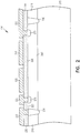
- the Hall element normally has an N-type accumulation layer on its surface due to the Qss in the surface oxide.
- the segments of the metal field plate are on top of this surface oxide layer.
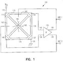
- the structure can be modeled as a Wheatstone bridge comprised of N-channel, depletion mode MOSFETs wherein the segments of the metal field plate act as the MOSFET gates. Changing the bias on the segments of the metal field plate changes the thickness of the surface accumulation layer, producing a change in the sheet conductivity of the N-type silicon.
- the quadrants of the Hall element representing the resistive branches of a Wheatstone bridge are modulated by the voltage potentials applied to the segments of the field plate.
- the field plates may cover substantially the entire Hall element, but should be at least partially electrically isolated from each other. In further embodiments, significantly less of the Hall element is covered by each of the field plates. In still further embodiments, more than four field plate segments may be utilized and electrical connections between them may be configured differently in various embodiments.
Landscapes
- Physics & Mathematics (AREA)
- Condensed Matter Physics & Semiconductors (AREA)
- General Physics & Mathematics (AREA)
- Hall/Mr Elements (AREA)
- Measuring Magnetic Variables (AREA)
Claims (9)
- Capteur Hall (100, 200) comprenant :un élément Hall (110, 240) supporté par un substrat,une couche isolante (220) disposée par-dessus l'élément Hall (110, 240),une plaque électriquement conductrice segmentée (160, 165, 170, 175) positionnée par-dessus l'élément Hall (110, 240), etdes lignes de rétroaction entre les sorties de détection (135, 140) de l'élément Hall (110, 240) et de la plaque électriquement conductrice segmentée (160, 165, 170, 175), caractérisé en ce que les lignes de rétroaction incluent un amplificateur différentiel (155) dont les entrées (145, 150) sont reliées aux sorties respectives (135, 140) dudit élément Hall, et dont les sorties (190, 195) sont ramenées vers ladite plaque électriquement conductrice segmentée (160, 165, 170, 175),dans lequel les sorties de capteur Hall sont reliées aux dites sorties (190, 195) dudit amplificateur (155).
- Capteur Hall (100, 200) selon la revendication 1, dans lequel la rétroaction provenant des lignes de rétroaction amène le capteur Hall (100, 200) à agir comme un circuit à verrouillage.
- Capteur Hall (100, 200) selon la revendication 1, dans lequel la rétroaction provenant des lignes de rétroaction amène une réponse linéaire du capteur Hall (100, 200).
- Capteur Hall (100, 200) selon la revendication 1, dans lequel la plaque électriquement conductrice segmentée (160, 165, 170, 175) comprend quatre segments.
- Capteur Hall (100, 200) selon la revendication 4, dans lequel l'élément Hall (110, 240) est de forme pratiquement rectangulaire et dans lequel les segments (160, 165, 170, 175) sont disposés dans quatre cadrans séparés définis par des droites s'étendant entre les coins opposés de l'élément Hall (110, 240).
- Capteur Hall (100, 200) selon la revendication 5, dans lequel les segments diagonaux opposés (160, 165, 170, 175) sont reliés électriquement, et dans lequel l'élément Hall (110, 240) comprend un coin de polarisation positive (115), un coin de polarisation négative (120), un coin de détection positive (135) et un coin de détection négative (140), et dans lequel un signal différentiel de rétroaction est délivré à la paire de segments opposés diagonalement, reliés électriquement (165, 170).
- Procédé destiné à un capteur Hall, caractérisé en ce qu'il comprend :la segmentation d'une plaque électriquement conductrice (160, 165, 170, 175) par-dessus un élément Hall (110, 240),l'isolement électrique (220) l'un de l'autre des segments (160, 165, 170, 175) de la plaque électriquement conductrice, etla délivrance d'une rétroaction (145, 150, 155, 190, 195) à des segments sélectionnés à partir des contacts de détection de l'élément Hall (110, 240), caractérisé par la délivrance de ladite rétroaction au travers d'un amplificateur différentiel (155) et de sorties (190, 195) .
- Procédé selon la revendication 7, dans lequel la rétroaction est positive, et lequel comprend en outre l'amplification de la rétroaction pour amener le verrouillage de l'élément Hall (110, 240).
- Procédé selon la revendication 7 et caractérisé en outre en ce qu'il comprend la commande de la rétroaction pour améliorer la linéarité.
Applications Claiming Priority (2)
| Application Number | Priority Date | Filing Date | Title |
|---|---|---|---|
| US10/826,746 US7015557B2 (en) | 2004-04-16 | 2004-04-16 | Hall element with segmented field plate |
| PCT/US2005/012672 WO2005106515A1 (fr) | 2004-04-16 | 2005-04-14 | Element hall a plaque a effet de champ segmentee |
Publications (2)
| Publication Number | Publication Date |
|---|---|
| EP1738191A1 EP1738191A1 (fr) | 2007-01-03 |
| EP1738191B1 true EP1738191B1 (fr) | 2019-08-14 |
Family
ID=34966360
Family Applications (1)
| Application Number | Title | Priority Date | Filing Date |
|---|---|---|---|
| EP05736873.0A Expired - Lifetime EP1738191B1 (fr) | 2004-04-16 | 2005-04-14 | Élément hall à plaque à effet de champ segmentée |
Country Status (5)
| Country | Link |
|---|---|
| US (1) | US7015557B2 (fr) |
| EP (1) | EP1738191B1 (fr) |
| JP (1) | JP2007532914A (fr) |
| CN (1) | CN1942775B (fr) |
| WO (1) | WO2005106515A1 (fr) |
Families Citing this family (13)
| Publication number | Priority date | Publication date | Assignee | Title |
|---|---|---|---|---|
| US7205622B2 (en) * | 2005-01-20 | 2007-04-17 | Honeywell International Inc. | Vertical hall effect device |
| WO2007116823A1 (fr) * | 2006-04-03 | 2007-10-18 | Asahi Kasei Emd Corporation | Element hall et capteur magnetique |
| WO2009036989A1 (fr) * | 2007-09-21 | 2009-03-26 | Inphynix | Unité de mesure de quantité physique et capteur pour mesures de champ électrique ou magnétique sans contact |
| US7626377B2 (en) * | 2008-02-18 | 2009-12-01 | Honeywell International Inc. | Hall-effect device with merged and/or non-merged complementary structure |
| EP2234185B1 (fr) * | 2009-03-24 | 2012-10-10 | austriamicrosystems AG | Capteur Hall vertical et procédé de production d'un capteur Hall vertical |
| US8384183B2 (en) * | 2010-02-19 | 2013-02-26 | Allegro Microsystems, Inc. | Integrated hall effect element having a germanium hall plate |
| WO2011148577A1 (fr) * | 2010-05-24 | 2011-12-01 | パナソニック株式会社 | Circuit d'élément formant orifice |
| JP5679906B2 (ja) | 2010-07-05 | 2015-03-04 | セイコーインスツル株式会社 | ホールセンサ |
| JP5815986B2 (ja) * | 2010-07-05 | 2015-11-17 | セイコーインスツル株式会社 | ホールセンサ |
| CN102790072A (zh) * | 2011-05-19 | 2012-11-21 | 上海腾怡半导体有限公司 | 集成霍尔器件及其制作方法 |
| US10120041B2 (en) * | 2015-03-27 | 2018-11-06 | Allegro Microsystems, Llc | Magnetic field sensor |
| US11782102B2 (en) * | 2021-10-22 | 2023-10-10 | Texas Instruments Incorporated | Hall sensor with dielectric isolation and p-n junction isolation |
| US12140646B2 (en) | 2023-02-06 | 2024-11-12 | Allegro Microsystems, Llc | Magnetic sensing having hall plate routing to reduce inductive coupling |
Family Cites Families (13)
| Publication number | Priority date | Publication date | Assignee | Title |
|---|---|---|---|---|
| US4048648A (en) | 1976-06-30 | 1977-09-13 | International Business Machines Corporation | High carrier velocity fet magnetic sensor |
| DE3435867A1 (de) | 1984-09-29 | 1986-04-10 | Bosch Gmbh Robert | Differentialsensor |
| JPH082631Y2 (ja) | 1988-08-05 | 1996-01-29 | 三菱電機株式会社 | ホール効果型センサ装置 |
| US5652445A (en) | 1995-04-21 | 1997-07-29 | Johnson; Mark B. | Hybrid hall effect device and method of operation |
| US6064083A (en) | 1995-04-21 | 2000-05-16 | Johnson; Mark B. | Hybrid hall effect memory device and method of operation |
| SE509206C2 (sv) | 1995-08-30 | 1998-12-14 | Roland Larsson | Vibrationsdetektor |
| US6195228B1 (en) | 1997-01-06 | 2001-02-27 | Nec Research Institute, Inc. | Thin, horizontal-plane hall sensors for read-heads in magnetic recording |
| US6265864B1 (en) | 1999-02-24 | 2001-07-24 | Melexis, N.V. | High speed densor circuit for stabilized hall effect sensor |
| US6492697B1 (en) | 2000-04-04 | 2002-12-10 | Honeywell International Inc. | Hall-effect element with integrated offset control and method for operating hall-effect element to reduce null offset |
| US6492679B1 (en) * | 2001-08-03 | 2002-12-10 | Semiconductor Components Industries Llc | Method for manufacturing a high voltage MOSFET device with reduced on-resistance |
| JP4417107B2 (ja) | 2001-10-01 | 2010-02-17 | 旭化成エレクトロニクス株式会社 | 磁気センサ |
| US6646315B1 (en) | 2002-04-22 | 2003-11-11 | The United States Of America As Represented By The Secretary Of The Navy | Conductive film layer for hall effect device |
| US6683359B2 (en) | 2002-06-21 | 2004-01-27 | The United States Of America As Represented By The Secretary Of The Navy | Hall effect device with multiple layers |
-
2004
- 2004-04-16 US US10/826,746 patent/US7015557B2/en not_active Expired - Lifetime
-
2005
- 2005-04-14 WO PCT/US2005/012672 patent/WO2005106515A1/fr not_active Ceased
- 2005-04-14 EP EP05736873.0A patent/EP1738191B1/fr not_active Expired - Lifetime
- 2005-04-14 CN CN2005800113263A patent/CN1942775B/zh not_active Expired - Fee Related
- 2005-04-14 JP JP2007508528A patent/JP2007532914A/ja not_active Withdrawn
Non-Patent Citations (1)
| Title |
|---|
| None * |
Also Published As
| Publication number | Publication date |
|---|---|
| EP1738191A1 (fr) | 2007-01-03 |
| US20050230769A1 (en) | 2005-10-20 |
| CN1942775B (zh) | 2012-07-04 |
| JP2007532914A (ja) | 2007-11-15 |
| CN1942775A (zh) | 2007-04-04 |
| US7015557B2 (en) | 2006-03-21 |
| WO2005106515A1 (fr) | 2005-11-10 |
Similar Documents
| Publication | Publication Date | Title |
|---|---|---|
| US7015557B2 (en) | Hall element with segmented field plate | |
| EP1269552B1 (fr) | Element a effet hall avec commande de decalage integree ; methode d'utilisation de l'element a effet hall pour reduire la tension de decalage nul | |
| KR940001298B1 (ko) | 집적회로에 집적가능한 홀소자를 구비한 장치 | |
| US7772661B2 (en) | Hall-effect magnetic sensors with improved magnetic responsivity and methods for manufacturing the same | |
| US4673964A (en) | Buried Hall element | |
| US4123772A (en) | Multisegment Hall element for offset voltage compensation | |
| Maupin et al. | The Hall effect in silicon circuits | |
| US20020003274A1 (en) | Piezoresistive sensor with epi-pocket isolation | |
| US4100563A (en) | Semiconductor magnetic transducers | |
| CN102608547A (zh) | 场效应磁传感器 | |
| GB2101402A (en) | Integrated overload protection circuit | |
| US3882409A (en) | Differential amplifier circuit | |
| US20180246147A1 (en) | Current sensing system and current sensing method | |
| US5920090A (en) | Switched magnetic field sensitive field effect transistor device | |
| JP2007532914A5 (fr) | ||
| JP2010175525A (ja) | 半導体磁気センサー | |
| JP3223387B2 (ja) | 電流検出機能付電界効果トランジスタ | |
| US10615333B2 (en) | Semiconductor device | |
| JP3453968B2 (ja) | 差動型半導体薄膜磁気抵抗素子 | |
| JP3182182B2 (ja) | 感磁性型半導体装置 | |
| JPH0691193B2 (ja) | 半導体装置 | |
| JP2632687B2 (ja) | 電力用半導体装置 | |
| JPS5955064A (ja) | ホ−ル素子 | |
| JPS6216029B2 (fr) | ||
| Roumenin et al. | New enhancing sensitivity tool for Hall effect devices |
Legal Events
| Date | Code | Title | Description |
|---|---|---|---|
| PUAI | Public reference made under article 153(3) epc to a published international application that has entered the european phase |
Free format text: ORIGINAL CODE: 0009012 |
|
| 17P | Request for examination filed |
Effective date: 20061013 |
|
| AK | Designated contracting states |
Kind code of ref document: A1 Designated state(s): DE FR GB |
|
| DAX | Request for extension of the european patent (deleted) | ||
| RBV | Designated contracting states (corrected) |
Designated state(s): DE FR GB |
|
| 17Q | First examination report despatched |
Effective date: 20110901 |
|
| RAP1 | Party data changed (applicant data changed or rights of an application transferred) |
Owner name: HONEYWELL INTERNATIONAL INC. |
|
| GRAP | Despatch of communication of intention to grant a patent |
Free format text: ORIGINAL CODE: EPIDOSNIGR1 |
|
| STAA | Information on the status of an ep patent application or granted ep patent |
Free format text: STATUS: GRANT OF PATENT IS INTENDED |
|
| INTG | Intention to grant announced |
Effective date: 20190211 |
|
| GRAS | Grant fee paid |
Free format text: ORIGINAL CODE: EPIDOSNIGR3 |
|
| GRAJ | Information related to disapproval of communication of intention to grant by the applicant or resumption of examination proceedings by the epo deleted |
Free format text: ORIGINAL CODE: EPIDOSDIGR1 |
|
| GRAL | Information related to payment of fee for publishing/printing deleted |
Free format text: ORIGINAL CODE: EPIDOSDIGR3 |
|
| STAA | Information on the status of an ep patent application or granted ep patent |
Free format text: STATUS: EXAMINATION IS IN PROGRESS |
|
| INTC | Intention to grant announced (deleted) | ||
| GRAP | Despatch of communication of intention to grant a patent |
Free format text: ORIGINAL CODE: EPIDOSNIGR1 |
|
| STAA | Information on the status of an ep patent application or granted ep patent |
Free format text: STATUS: GRANT OF PATENT IS INTENDED |
|
| GRAA | (expected) grant |
Free format text: ORIGINAL CODE: 0009210 |
|
| STAA | Information on the status of an ep patent application or granted ep patent |
Free format text: STATUS: THE PATENT HAS BEEN GRANTED |
|
| INTG | Intention to grant announced |
Effective date: 20190703 |
|
| AK | Designated contracting states |
Kind code of ref document: B1 Designated state(s): DE FR GB |
|
| REG | Reference to a national code |
Ref country code: GB Ref legal event code: FG4D |
|
| REG | Reference to a national code |
Ref country code: DE Ref legal event code: R096 Ref document number: 602005056143 Country of ref document: DE |
|
| REG | Reference to a national code |
Ref country code: DE Ref legal event code: R097 Ref document number: 602005056143 Country of ref document: DE |
|
| PLBE | No opposition filed within time limit |
Free format text: ORIGINAL CODE: 0009261 |
|
| STAA | Information on the status of an ep patent application or granted ep patent |
Free format text: STATUS: NO OPPOSITION FILED WITHIN TIME LIMIT |
|
| 26N | No opposition filed |
Effective date: 20200603 |
|
| REG | Reference to a national code |
Ref country code: DE Ref legal event code: R119 Ref document number: 602005056143 Country of ref document: DE |
|
| PG25 | Lapsed in a contracting state [announced via postgrant information from national office to epo] |
Ref country code: DE Free format text: LAPSE BECAUSE OF NON-PAYMENT OF DUE FEES Effective date: 20201103 |
|
| PGFP | Annual fee paid to national office [announced via postgrant information from national office to epo] |
Ref country code: GB Payment date: 20240423 Year of fee payment: 20 |
|
| PGFP | Annual fee paid to national office [announced via postgrant information from national office to epo] |
Ref country code: FR Payment date: 20240430 Year of fee payment: 20 |
|
| REG | Reference to a national code |
Ref country code: GB Ref legal event code: PE20 Expiry date: 20250413 |
|
| PG25 | Lapsed in a contracting state [announced via postgrant information from national office to epo] |
Ref country code: GB Free format text: LAPSE BECAUSE OF EXPIRATION OF PROTECTION Effective date: 20250413 |