EP1739747A2 - Halbleiterchip und Verfahren zur Herstellung - Google Patents
Halbleiterchip und Verfahren zur Herstellung Download PDFInfo
- Publication number
- EP1739747A2 EP1739747A2 EP06013661A EP06013661A EP1739747A2 EP 1739747 A2 EP1739747 A2 EP 1739747A2 EP 06013661 A EP06013661 A EP 06013661A EP 06013661 A EP06013661 A EP 06013661A EP 1739747 A2 EP1739747 A2 EP 1739747A2
- Authority
- EP
- European Patent Office
- Prior art keywords
- semiconductor substrate
- semiconductor chip
- external connection
- wiring pattern
- hole
- Prior art date
- Legal status (The legal status is an assumption and is not a legal conclusion. Google has not performed a legal analysis and makes no representation as to the accuracy of the status listed.)
- Withdrawn
Links
Images





Classifications
-
- H—ELECTRICITY
- H10—SEMICONDUCTOR DEVICES; ELECTRIC SOLID-STATE DEVICES NOT OTHERWISE PROVIDED FOR
- H10W—GENERIC PACKAGES, INTERCONNECTIONS, CONNECTORS OR OTHER CONSTRUCTIONAL DETAILS OF DEVICES COVERED BY CLASS H10
- H10W70/00—Package substrates; Interposers; Redistribution layers [RDL]
- H10W70/60—Insulating or insulated package substrates; Interposers; Redistribution layers
-
- H—ELECTRICITY
- H10—SEMICONDUCTOR DEVICES; ELECTRIC SOLID-STATE DEVICES NOT OTHERWISE PROVIDED FOR
- H10W—GENERIC PACKAGES, INTERCONNECTIONS, CONNECTORS OR OTHER CONSTRUCTIONAL DETAILS OF DEVICES COVERED BY CLASS H10
- H10W20/00—Interconnections in chips, wafers or substrates
- H10W20/40—Interconnections external to wafers or substrates, e.g. back-end-of-line [BEOL] metallisations or vias connecting to gate electrodes
-
- H—ELECTRICITY
- H10—SEMICONDUCTOR DEVICES; ELECTRIC SOLID-STATE DEVICES NOT OTHERWISE PROVIDED FOR
- H10D—INORGANIC ELECTRIC SEMICONDUCTOR DEVICES
- H10D64/00—Electrodes of devices having potential barriers
- H10D64/01—Manufacture or treatment
- H10D64/011—Manufacture or treatment of electrodes ohmically coupled to a semiconductor
-
- H—ELECTRICITY
- H10—SEMICONDUCTOR DEVICES; ELECTRIC SOLID-STATE DEVICES NOT OTHERWISE PROVIDED FOR
- H10W—GENERIC PACKAGES, INTERCONNECTIONS, CONNECTORS OR OTHER CONSTRUCTIONAL DETAILS OF DEVICES COVERED BY CLASS H10
- H10W20/00—Interconnections in chips, wafers or substrates
- H10W20/01—Manufacture or treatment
- H10W20/021—Manufacture or treatment of interconnections within wafers or substrates
- H10W20/023—Manufacture or treatment of interconnections within wafers or substrates the interconnections being through-semiconductor vias
- H10W20/0234—Manufacture or treatment of interconnections within wafers or substrates the interconnections being through-semiconductor vias comprising etching via holes that stop on pads or on electrodes
-
- H—ELECTRICITY
- H10—SEMICONDUCTOR DEVICES; ELECTRIC SOLID-STATE DEVICES NOT OTHERWISE PROVIDED FOR
- H10W—GENERIC PACKAGES, INTERCONNECTIONS, CONNECTORS OR OTHER CONSTRUCTIONAL DETAILS OF DEVICES COVERED BY CLASS H10
- H10W20/00—Interconnections in chips, wafers or substrates
- H10W20/01—Manufacture or treatment
- H10W20/021—Manufacture or treatment of interconnections within wafers or substrates
- H10W20/023—Manufacture or treatment of interconnections within wafers or substrates the interconnections being through-semiconductor vias
- H10W20/0238—Manufacture or treatment of interconnections within wafers or substrates the interconnections being through-semiconductor vias comprising etching via holes through pads or through electrodes
-
- H—ELECTRICITY
- H10—SEMICONDUCTOR DEVICES; ELECTRIC SOLID-STATE DEVICES NOT OTHERWISE PROVIDED FOR
- H10W—GENERIC PACKAGES, INTERCONNECTIONS, CONNECTORS OR OTHER CONSTRUCTIONAL DETAILS OF DEVICES COVERED BY CLASS H10
- H10W20/00—Interconnections in chips, wafers or substrates
- H10W20/01—Manufacture or treatment
- H10W20/021—Manufacture or treatment of interconnections within wafers or substrates
- H10W20/023—Manufacture or treatment of interconnections within wafers or substrates the interconnections being through-semiconductor vias
- H10W20/0242—Manufacture or treatment of interconnections within wafers or substrates the interconnections being through-semiconductor vias comprising etching via holes from the back sides of the chips, wafers or substrates
-
- H—ELECTRICITY
- H10—SEMICONDUCTOR DEVICES; ELECTRIC SOLID-STATE DEVICES NOT OTHERWISE PROVIDED FOR
- H10W—GENERIC PACKAGES, INTERCONNECTIONS, CONNECTORS OR OTHER CONSTRUCTIONAL DETAILS OF DEVICES COVERED BY CLASS H10
- H10W20/00—Interconnections in chips, wafers or substrates
- H10W20/20—Interconnections within wafers or substrates, e.g. through-silicon vias [TSV]
-
- H—ELECTRICITY
- H10—SEMICONDUCTOR DEVICES; ELECTRIC SOLID-STATE DEVICES NOT OTHERWISE PROVIDED FOR
- H10W—GENERIC PACKAGES, INTERCONNECTIONS, CONNECTORS OR OTHER CONSTRUCTIONAL DETAILS OF DEVICES COVERED BY CLASS H10
- H10W20/00—Interconnections in chips, wafers or substrates
- H10W20/20—Interconnections within wafers or substrates, e.g. through-silicon vias [TSV]
- H10W20/211—Through-semiconductor vias, e.g. TSVs
- H10W20/213—Cross-sectional shapes or dispositions
- H10W20/2134—TSVs extending from the semiconductor wafer into back-end-of-line layers
Definitions
- the present disclosure relates to a semiconductor chip and a method of manufacturing the same. More particularly, the present disclosure relates to a semiconductor chip, which is stacked together with other semiconductor chips and electrically connected with other semiconductor chips, and a method of manufacturing the same.
- a plurality of semiconductor chips are stacked and electrically connected mutually. Through vias that are passed through the semiconductor chips and connected electrically to external connection terminals provided on the semiconductor chips are formed in these plural semiconductor chips (see FIG.22).
- FIG.22 is a sectional view of a semiconductor chip having the through vias in the related art.
- a semiconductor chip 100 has a semiconductor substrate 101, insulating films 102, 105, 108, a multi-layered wiring structure 103, external connection terminals 104, through holes 107, and through vias 109.
- the insulating film 102 is provided on the thinned semiconductor substrate 101.
- the insulating film 102 insulates wirings 112 provided in the multi-layered wiring structure 103 from the semiconductor substrate 101.
- the multi-layered wiring structure 103 is constructed by a plurality of laminated insulating layers 111, the wirings 112, and vias 113.
- the external connection terminals 104 are provided to an uppermost layer of the multi-layered wiring structure 103.
- the insulating film 105 is provided to expose the external connection terminals 104 and cover the upper surface of the multi-layered wiring structure 103.
- the through holes 107 are formed to pass through the semiconductor substrate 101 and the multi-layered wiring structure 103 and expose the external connection terminals 104.
- the insulating film 108 is provided to cover a side surface of the through hole 107.
- the insulating film 108 insulates the through via 109 from the semiconductor substrate 101.
- the through vias 109 are provided in the through holes 107 on which the insulating film 108 is formed respectively.
- the through vias 109 connect electrically a back surface 101B of the semiconductor substrate 101 and the external connection terminals 104.
- FIG.23 to FIG.27 are views showing steps of manufacturing a semiconductor chip in the related art.
- the same reference symbols are affixed to the same constituent portions as the semiconductor chip 100 explained in FIG.22.
- the semiconductor chip 100 Next, a method of manufacturing the semiconductor chip 100 will be explained with reference to FIG.23 to FIG.27 hereunder.
- the insulating films 102, 105, the multi-layered wiring structure 103, and the external connection terminals 104 are formed on the semiconductor substrate 101, and then the semiconductor substrate 101 is thinned from the back surface 101B side.
- the through holes 107 for exposing the external connection terminals 104 are formed from the back surface 101B side of the semiconductor substrate 101 by the dry etching method.
- the insulating film 108 is formed on the through holes 107 respectively.
- the unnecessary insulating film 108 provided on the external connection terminals 104 is removed respectively.
- the through vias 109 are formed in the through holes 107 on which the insulating film 108 is formed respectively. Accordingly, the semiconductor chip 100 is manufactured (see Japanese Patent Unexamined Publication No. 2001-60654 , for example).
- the semiconductor chip 100 in the related art a plurality of different materials (e.g., the insulating film 102, the insulating layers 111, the wirings 112, and the like) must be etched upon forming the through holes 107. Therefore, it was difficult to form the through holes 107.
- a plurality of different materials e.g., the insulating film 102, the insulating layers 111, the wirings 112, and the like
- the present invention intends to overcome at least some of the above problems.
- the object is solved by the semiconductor chip according to independent claim 1 and by the method of manufacturing a semiconductor chip according to independent claim 4. Further advantages, features, aspects and details of the invention are evident from the dependent claims, the description and the drawings.
- a semiconductor chip includes a semiconductor substrate; a multi-layered wiring structure having a plurality of insulating layers laminated on the semiconductor substrate, and a first wiring pattern provided in the plurality of insulating layers; and an external connection terminal provided on an uppermost layer of the multi-layered wiring structure; wherein a through via is provided in the through hole that passes through the semiconductor substrate, and a second wiring pattern for connecting electrically the through via and the external connection terminal is provided in the plurality of insulating layers.
- the through hole in which the through via is provided may be formed to pass through only the semiconductor substrate. Therefore, a production cost of the semiconductor chip can be reduced by forming easily the through hole rather than the related art.
- a method of manufacturing a semiconductor chip that includes a semiconductor substrate that includes a semiconductor substrate, a multi-layered wiring structure having a plurality of insulating layers laminated on the semiconductor substrate and a first wiring pattern provided in the plurality of insulating layers, an external connection terminal provided on an uppermost layer of the multi-layered wiring structure, a through via provided in a through hole that passes through the semiconductor substrate, and a second wiring pattern provided in the plurality of insulating layers to connect electrically the through via and the external connection terminal, includes steps of: forming simultaneously the first wiring pattern and the second wiring pattern on the semiconductor substrate; forming the through hole, which exposes the second wiring pattern, in the semiconductor substrate; forming an insulating film on a side surface of the through hole; and forming the through via in a through hole on which the insulating film is formed.
- a semiconductor chip includes a semiconductor substrate, a through via provided in a through hole that passes through the semiconductor substrate, insulating layers, preferably at least three insulating layers, laminated on the semiconductor substrate, a multi-layered wiring structure having a first wiring pattern and a second wiring pattern, and an external connection terminal provided on an uppermost layer of the multi-layered wiring structure, wherein the through via and the external connection terminal are connected electrically by the second wiring pattern.
- the through hole can be formed as the through hole that passes through merely the semiconductor substrate. Therefore, the through hole can be formed easily by one etching step, and thus a production cost of the semiconductor chip can be reduced. Also, since the second wiring pattern that connects electrically the external connection terminal and the through via can be formed simultaneously with the first wiring pattern, an increase of a production cost can be suppressed.
- Various implementations may include one or more the following advantages. For example, a production cost can be reduced by forming easily through holes used to provide through vias that are connected electrically to external connection terminals. Other features and advantages may be apparent from the following detailed description, the accompanying drawings and the claims.
- the invention is also directed to apparatuses for carrying out the disclosed methods and including apparatus parts for performing each described method steps. These method steps may be performed by way of hardware components, a computer programmed by appropriate software, by any combination of the two or in any other manner. It further includes method steps for manufacturing every part of the semiconductor chip.
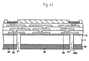
- FIG.1 is a sectional view of a semiconductor chip according to an embodiment of the present invention.
- a semiconductor chip 10 includes a plurality of semiconductor elements (not shown) each of which consists of a semiconductor substrate 11, through vias 12, insulating films 13, 18, a multi-layered wiring structure 14, external connection terminals 15, a protection film 16, transistors, and the like.
- the semiconductor substrate 11 is thinned, and through holes 17 used to provide the through vias 12 are formed in the semiconductor substrate 11.
- a silicon substrate can be employed by way of example.
- a compound semiconductor such as GaAs, or the like may be employed other than the silicon substrate.
- a thickness M1 of the semiconductor substrate 11 can be set to 200 ⁇ m, for example.
- the through via 12 is provided in the through hole 17 via the insulating film 18 made of SiO 2 , as an example.
- the through via 12 is passed through the semiconductor substrate 11, and one end of the through via 12 is exposed from a back surface 11B of the semiconductor substrate 11 and the other end is connected electrically to a second wiring pattern 23 described later.
- the material of the through via 12 for example, Cu may be employed.
- a diameter R1 of the through via 12 can be set to 50 ⁇ m, for example.
- the insulating film 13 is made of SiO 2 , for example, and is provided to cover a surface 11A of the semiconductor substrate 11. Opening portions 13A for exposing the through vias 12 are formed in portions of the insulating film 13 opposing to the through vias 12. A diameter R2 of the opening portion 13A can be set to 70 ⁇ m, for example.
- the multi-layered wiring structure 14 is provided on the surface 11A of the semiconductor substrate 11, and has a plurality of (in the present embodiment, three) laminated insulating layers 21-1 to 21-3 and a first wiring pattern 22 and the second wiring pattern 23.
- the insulating layers 21-1 to 21-3 are laminated on the surface 11A of the semiconductor substrate 11 in order of the insulating layer 21-1, the insulating layer 21-2, and the insulating layer 21-3.
- an inorganic insulating film can be employed, and more particularly an SiO 2 film can be employed.
- the first wiring patterns 22 are provided to the insulating layers 21-1 to 21-3, and are stacked alternately in a state that a plurality of wirings 25 and vias 26 are connected electrically.
- the first wiring pattern 22 is provided in the semiconductor chip 10 in the related art and is the wiring pattern used to improve the integration density of the semiconductor chip 10. Also, the first wiring pattern 22 connect electrically a plurality of semiconductor elements (not shown) formed of a transistor, or the like to constitute a semiconductor circuit.
- the second wiring pattern 23 is provided in the insulating film 13 and the insulating layers 21-1 to 21-3 to connect electrically the through via 12 and the external connection terminal 15 formed on the insulating layer 21-3.
- the second wiring pattern 23 is constructed by stacking sequentially a via 28A, a wiring 29, a via 28B, the wiring 29, the via 28B, the wiring 29, a via 28C such that the via 28A and the via 28C are connected electrically. Also, although not shown, the second wiring pattern may be connected electrically to the first wiring pattern.
- the via 28A is provided in the opening portion 13A formed in the insulating film 13.
- the via 28C is connected electrically to the external connection terminal 15.
- the through holes 17 in which the through vias 12 are provided may be formed to pass through only the semiconductor substrate 11. Therefore, a production cost of the semiconductor chip 10 can be reduced by forming easily the through holes 17 rather than the related art.
- the external connection terminals 15 are provided on portions of the insulating layer 21-3 corresponding to forming positions of the vias 28C.
- the external connection terminals 15 are connected electrically to the vias 28C.
- the protection film 16 is provided to cover the insulating layer 21-3 in a state that the external connection terminals 15 are exposed.
- the protection film 16 for example, an SiO 2 film, an SiN film, a polyimide resin, or the like can be employed.
- the through holes 17 in which the through vias 12 are provided may be formed to pass through only the semiconductor substrate 11. Therefore, a production cost of the semiconductor chip 10 can be reduced by forming easily the through holes 17 in contrast to the related art.
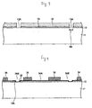
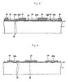
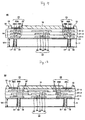
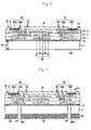
- FIG.2 to FIG.16 are views showing steps of manufacturing the semiconductor chip according to the present embodiment.
- the same reference symbols are affixed to the same constituent portions as those in the semiconductor chip 10 explained in FIG.1.
- the insulating film 13 and a resist film 32 having opening portions 32A each corresponding to a shape of the via 28A are formed sequentially on the semiconductor substrate 11 before a thickness of such substrate is reduced.
- the semiconductor substrate 11 for example, a silicon wafer can be employed.
- the opening portions 13A for exposing the semiconductor substrate 11 are formed in the insulating film 13 by etching the insulating film 13 using the resist film 32 as a mask.
- a diameter R2 of the opening portion 13A can be set to 70 ⁇ m, for example.
- the resist film 32 is removed by a resist remover after the opening portions 13A are formed.
- a seed layer 33 is formed on portions of the semiconductor substrate 11 corresponding to the opening portions 13A and the insulating film 13.
- a Ti/Cu laminated film in which a Ti layer and a Cu layer are laminated sequentially by a sputter method, an evaporation method, an electroless plating method, or the like, for example, can be employed.
- a resist film 34 having opening portions 34A and opening portions 34B is formed on the seed layer 33.
- This opening portion 34A exposes a forming area of the first wiring pattern 22 (in this case, forming area of the wiring 25), and this opening portion 34B exposes a forming area of the second wiring pattern 23 (in this case, forming areas of the via 28A and the wiring 29).
- a plating film is deposited on the seed layer 33 by the electroplating method.
- the wiring 25 (the first wiring pattern 22) is formed on portions of the seed layer 33 corresponding to the opening portions 34A and simultaneously the via 28A and the wiring 29 (the second wiring pattern 23) are formed on portions of the seed layer 33 corresponding to the opening portion 34B.
- a Cu plating film can be employed as the wirings 25, 29 and the via 28A.
- the resist film 34 is removed by the resist remover, and then the seed layer 33 is removed.
- the vias 28B, 26 and the wirings 25, 29 are formed simultaneously on the insulating layer 21-1 by the same approach as steps in FIG.4 to FIG.6 explained as above.
- the insulating layer 21-2 is formed by the same approach as step in FIG.7.
- the multi-layered wiring structure 14 having the laminated insulating layers 21-1 to 21-3, the first wiring pattern 22, and the second wiring pattern 23 is formed by repeating steps in FIG.4 to FIG.7.
- the vias 28B, 26 for example, a Cu plating film can be employed.
- the SiO 2 film formed by the CVD method can be employed as the insulating layers 21-1 to 21-3.
- the external connection terminals 15 are formed on portions of the insulating layer 21-3 corresponding to forming positions of the vias 28C, and then the protection film 16 for exposing the external connection terminal 15 and covering an upper surface of the insulating layer 21-3 is formed.
- an Al film (thickness 0.5 ⁇ m) acting as the external connection terminal 15 is formed by the sputter method, and then a polyimide resin film acting as the protection film 16 is formed by the spin coating method, the spray method, the dipping method, or the like.
- the semiconductor substrate 11 is thinned from the back surface 11B side of the semiconductor substrate 11 (semiconductor substrate thinning step).
- semiconductor substrate thinning step for example, a backside grinder can be employed.
- a thickness M1 of the thinned semiconductor substrate 11 can be set to 200 ⁇ m, for example.
- an aspect ratio (thickness M1 of the semiconductor substrate 11/diameter of the through hole 17) of the through hole 17 can be reduced by reducing a thickness of the semiconductor substrate 11, and thus the through holes 17 can be formed with good precision.
- the semiconductor substrate 11 may be thinned by using the grinding method except the grinder.
- the through holes 17, which pass through the semiconductor substrate 11 and expose the via 28A of the second wiring pattern 23, are formed by the dry etching method using the resist layer 36 as a mask (through hole forming step).
- the resist layer 36 is removed by the resist remover after the through holes 17 are formed.
- the through holes 17 that pass through only the semiconductor substrate 11 can be formed easily by the etching at a time. Therefore, a production cost of the semiconductor chip 10 can be reduced.
- the insulating film 18 is formed on the through holes 17 and the back surface 11B respectively (insulating film forming step) . More particularly, for example, the SiO 2 film is formed by the CVD method. Then, in step in FIG.15, the insulating film 18 provided on the via 28A is removed.
- the dry etching method, the wet etching method, or the like can be employed to remove the insulating film 18.
- a KOH solution can be employed as an etching solution of the wet etching method.
- the through vias 12 are formed by filling the conductive material into the through holes 17 on which the insulating film 18 is provided respectively (through via forming step). More particularly, the Ti/Cu laminated film acting as the seed layer (not shown) is formed by the sputter method to cover a lower surface of a resultant structure shown in FIG. 15 and the through holes 17 on which the insulating film 18 is provided respectively, then the resist film having the opening portions from which the through holes 17 are exposed is formed on the lower surface of the resultant structure shown in FIG.15, then the conductive material is filled into the through holes 17 by the electroplating method using the seed layer as a power feeding layer, and then the resist film and the unnecessary Ti/Cu laminated film are removed sequentially.
- pads may be formed on edge portions of the through holes 17 by forming the opening portions in the resist film to expose the insulating film 18 around the through holes 17.
- wirings connected electrically to the through vias 12 may be formed on the lower surface of the resultant structure shown in FIG.15 by forming opening portions corresponding to wiring shapes in the resist film.
- the seed layer may be formed by the evaporation method or the electroless plating method other than the sputter method.
- the conductive material for example, Cu can be employed.
- a diameter R1 of the through via 12 can be set to 50 ⁇ m, for example.
- the through holes 17 that passes through merely the semiconductor substrate 11 can be formed easily by one etching step, and thus a production cost of the semiconductor chip 10 can be reduced.
- the second wiring patterns 23 that connect electrically the external connection terminal 15 and the through via 12 respectively can be formed simultaneously with the first wiring patterns 22, and thus an increase of a production cost can be suppressed.
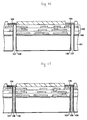
- FIG.17 is a sectional view of a semiconductor chip according to a first variation of the present embodiment.
- the same reference symbols are affixed to the same constituent portions as the semiconductor chip 10 of the present embodiment, and their explanation will be omitted herein.
- a semiconductor chip 40 is constructed in the same manner as the semiconductor chip 10 except that the through vias 12 are provided in portions of the semiconductor substrate 11 positioned almost directly under the external connection terminals 15 and also a plurality of vias 28A to 28C are arranged in a plurality of insulating layers 21-1 to 21-3, which are positioned between the through via 12 and the external connection terminals 15, to intersect almost orthogonally with the surface of the semiconductor substrate 11.
- a plurality of vias 28A to 28C are arranged in a plurality of insulating layers 21-1 to 21-3, which are positioned between the through via 12 and the external connection terminals 15, to intersect almost orthogonally with the surface of the semiconductor substrate 11. Therefore, a wiring length of the second wiring pattern 23 that connects the external connection terminals 15 and the through via 12 can be shortened, so that the semiconductor chip 40 can be operated at a high speed. In this case, the semiconductor chip 40 can be manufactured by the same approach as the semiconductor chip 10 explained above.
- FIG.18 is a sectional view of a semiconductor chip according to a second variation of the present embodiment.
- the same reference symbols are affixed to the same constituent portions as the semiconductor chip 10 of the present embodiment, and their explanation will be omitted herein.
- a semiconductor chip 50 is constructed in the same manner as the semiconductor chip 10 except that through vias 52 and second wiring patterns 53 are provided instead of the through vias 12 and the second wiring patterns 23.
- the through vias 52 are provided in through holes 51 that pass through the thinned semiconductor substrate 11 and the insulating film 13.
- the through hole 51 exposes the wiring 29 provided on the insulating film 13.
- the same material as the through via 12 can be employed.
- the second wiring patterns 53 are constructed in the same manner as the second wiring patterns 23 except that the via 28A is removed from the structure of the second wiring pattern 23.
- the wiring 29 provided on the insulating film 13 is connected electrically to the through via 52.
- FIG.19 to FIG.21 are views showing steps of manufacturing a semiconductor chip according to the second variation of the present embodiment.
- the same reference symbols are affixed to the same constituent portions as the semiconductor chip 50 explained in FIG.18.
- the insulating film 13, the first and second wiring patterns 22, 53, the insulating layers 21-1 to 21-3, the external connection terminals 15, and the protection film 16 are formed on the semiconductor substrate 11 (containing the first and second wiring pattern forming step). Then, the semiconductor substrate 11 is thinned up to a thickness M1 (semiconductor substrate thinning step).
- the first and second wiring patterns 22, 53 are formed by the same approach as the steps shown in FIG.4 to FIG.9 explained above.
- the through holes 51 from which the wiring 29 is exposed are formed by removing the insulating film 13 that is exposed from the semiconductor substrate 11.
- the dry etching method, the wet etching method, the laser method, or the like can be employed.
- the insulating film 18 for covering side surfaces of the through holes 51 and the back surface 11B is formed and then the through vias 52 are formed in the through holes 51 on which the insulating film 18 is formed respectively (through via forming step).
- the semiconductor chip 50 is manufactured.
- the present invention is applicable to a semiconductor chip that is capable of reducing a production cost by forming easily through holes used to provide through vias that are connected electrically to external connection terminals, and a method of manufacturing the same.
Landscapes
- Internal Circuitry In Semiconductor Integrated Circuit Devices (AREA)
Applications Claiming Priority (1)
| Application Number | Priority Date | Filing Date | Title |
|---|---|---|---|
| JP2005191407A JP4250154B2 (ja) | 2005-06-30 | 2005-06-30 | 半導体チップ及びその製造方法 |
Publications (2)
| Publication Number | Publication Date |
|---|---|
| EP1739747A2 true EP1739747A2 (de) | 2007-01-03 |
| EP1739747A3 EP1739747A3 (de) | 2007-08-01 |
Family
ID=37054435
Family Applications (1)
| Application Number | Title | Priority Date | Filing Date |
|---|---|---|---|
| EP06013661A Withdrawn EP1739747A3 (de) | 2005-06-30 | 2006-06-30 | Halbleiterchip und Verfahren zur Herstellung |
Country Status (4)
| Country | Link |
|---|---|
| US (2) | US7843068B2 (de) |
| EP (1) | EP1739747A3 (de) |
| JP (1) | JP4250154B2 (de) |
| KR (1) | KR101178823B1 (de) |
Cited By (1)
| Publication number | Priority date | Publication date | Assignee | Title |
|---|---|---|---|---|
| CN103597916A (zh) * | 2012-03-27 | 2014-02-19 | 松下电器产业株式会社 | 增层基板及其制造方法、以及半导体集成电路封装件 |
Families Citing this family (28)
| Publication number | Priority date | Publication date | Assignee | Title |
|---|---|---|---|---|
| JP2008210952A (ja) * | 2007-02-26 | 2008-09-11 | Sanyo Electric Co Ltd | 半導体装置の製造方法、シリコンインターポーザの製造方法および半導体モジュールの製造方法 |
| JP4809308B2 (ja) * | 2007-09-21 | 2011-11-09 | 新光電気工業株式会社 | 基板の製造方法 |
| KR101374338B1 (ko) * | 2007-11-14 | 2014-03-14 | 삼성전자주식회사 | 관통 전극을 갖는 반도체 장치 및 그 제조방법 |
| JP2009224492A (ja) * | 2008-03-14 | 2009-10-01 | Oki Semiconductor Co Ltd | 半導体装置及びその製造方法 |
| KR101458958B1 (ko) * | 2008-06-10 | 2014-11-13 | 삼성전자주식회사 | 반도체 칩, 반도체 패키지 및 반도체 칩의 제조 방법 |
| US8227889B2 (en) * | 2008-12-08 | 2012-07-24 | United Microelectronics Corp. | Semiconductor device |
| US7910473B2 (en) | 2008-12-31 | 2011-03-22 | Taiwan Semiconductor Manufacturing Company, Ltd. | Through-silicon via with air gap |
| US8399354B2 (en) | 2009-01-13 | 2013-03-19 | Taiwan Semiconductor Manufacturing Company, Ltd. | Through-silicon via with low-K dielectric liner |
| JP2010205921A (ja) * | 2009-03-03 | 2010-09-16 | Olympus Corp | 半導体装置および半導体装置の製造方法 |
| JP2010232400A (ja) * | 2009-03-27 | 2010-10-14 | Panasonic Corp | 半導体基板と半導体基板の製造方法および半導体パッケージ |
| US8222739B2 (en) | 2009-12-19 | 2012-07-17 | International Business Machines Corporation | System to improve coreless package connections |
| JP5426417B2 (ja) | 2010-02-03 | 2014-02-26 | ルネサスエレクトロニクス株式会社 | 半導体装置およびその製造方法 |
| JP2011171567A (ja) * | 2010-02-19 | 2011-09-01 | Elpida Memory Inc | 基板構造物の製造方法及び半導体装置の製造方法 |
| JP5412316B2 (ja) * | 2010-02-23 | 2014-02-12 | パナソニック株式会社 | 半導体装置、積層型半導体装置及び半導体装置の製造方法 |
| JP2011238742A (ja) * | 2010-05-10 | 2011-11-24 | Shinko Electric Ind Co Ltd | 配線基板の製造方法及び配線基板 |
| US20120248621A1 (en) * | 2011-03-31 | 2012-10-04 | S.O.I.Tec Silicon On Insulator Technologies | Methods of forming bonded semiconductor structures, and semiconductor structures formed by such methods |
| US8338294B2 (en) * | 2011-03-31 | 2012-12-25 | Soitec | Methods of forming bonded semiconductor structures including two or more processed semiconductor structures carried by a common substrate, and semiconductor structures formed by such methods |
| JP2012222161A (ja) * | 2011-04-08 | 2012-11-12 | Elpida Memory Inc | 半導体装置 |
| US8587127B2 (en) * | 2011-06-15 | 2013-11-19 | Taiwan Semiconductor Manufacturing Company, Ltd. | Semiconductor structures and methods of forming the same |
| US9111998B2 (en) | 2012-04-04 | 2015-08-18 | Samsung Electronics Co., Ltd | Multi-level stack having multi-level contact and method |
| JP6175701B2 (ja) * | 2012-06-04 | 2017-08-09 | マクロニックス インターナショナル カンパニー リミテッド | 3d積層マルチチップモジュールの製造方法 |
| US9287162B2 (en) | 2013-01-10 | 2016-03-15 | Samsung Austin Semiconductor, L.P. | Forming vias and trenches for self-aligned contacts in a semiconductor structure |
| US20160300764A1 (en) * | 2013-07-05 | 2016-10-13 | Hitachi, Ltd. | Semiconductor device and method for manufacturing the same |
| KR102094473B1 (ko) | 2013-10-15 | 2020-03-27 | 삼성전자주식회사 | Tsv 구조를 구비한 집적회로 소자 및 그 제조 방법 |
| JP2016058628A (ja) * | 2014-09-11 | 2016-04-21 | 株式会社東芝 | 半導体装置、及び半導体装置の製造方法 |
| JP2017009704A (ja) * | 2015-06-18 | 2017-01-12 | キヤノン株式会社 | 多層膜を用いた光学素子、光学系および光学機器 |
| KR102793910B1 (ko) | 2020-03-26 | 2025-04-08 | 삼성전자주식회사 | 관통 실리콘 비아를 포함하는 집적 회로 반도체 소자 |
| KR102949121B1 (ko) | 2021-05-14 | 2026-04-03 | 삼성전자주식회사 | 집적회로 소자 및 이를 포함하는 반도체 패키지 |
Family Cites Families (20)
| Publication number | Priority date | Publication date | Assignee | Title |
|---|---|---|---|---|
| JPS6423564A (en) | 1987-07-17 | 1989-01-26 | Sharp Kk | Space type semiconductor device |
| JPH0533645Y2 (de) | 1987-07-31 | 1993-08-26 | ||
| JPH0529483A (ja) | 1991-07-19 | 1993-02-05 | Rohm Co Ltd | 半導体集積装置 |
| JPH0964050A (ja) | 1995-08-29 | 1997-03-07 | Hitachi Ltd | 半導体素子およびその製造方法 |
| JP3184493B2 (ja) | 1997-10-01 | 2001-07-09 | 松下電子工業株式会社 | 電子装置の製造方法 |
| JP3563604B2 (ja) * | 1998-07-29 | 2004-09-08 | 株式会社東芝 | マルチチップ半導体装置及びメモリカード |
| JP3726579B2 (ja) | 1999-08-20 | 2005-12-14 | セイコーエプソン株式会社 | 半導体装置およびその製造方法 |
| US6882045B2 (en) | 1999-10-28 | 2005-04-19 | Thomas J. Massingill | Multi-chip module and method for forming and method for deplating defective capacitors |
| JP3779524B2 (ja) * | 2000-04-20 | 2006-05-31 | 株式会社東芝 | マルチチップ半導体装置及びメモリカード |
| JP4123682B2 (ja) | 2000-05-16 | 2008-07-23 | セイコーエプソン株式会社 | 半導体装置及びその製造方法 |
| US6444576B1 (en) | 2000-06-16 | 2002-09-03 | Chartered Semiconductor Manufacturing, Ltd. | Three dimensional IC package module |
| KR100364635B1 (ko) * | 2001-02-09 | 2002-12-16 | 삼성전자 주식회사 | 칩-레벨에 형성된 칩 선택용 패드를 포함하는 칩-레벨3차원 멀티-칩 패키지 및 그 제조 방법 |
| US6495912B1 (en) * | 2001-09-17 | 2002-12-17 | Megic Corporation | Structure of ceramic package with integrated passive devices |
| EP2560199B1 (de) * | 2002-04-05 | 2016-08-03 | STMicroelectronics S.r.l. | Verfahren zum Herstellen einer durchisolierten Verbindung in einem Körper aus einem Halbleitermaterial |
| US7030481B2 (en) * | 2002-12-09 | 2006-04-18 | Internation Business Machines Corporation | High density chip carrier with integrated passive devices |
| JP4327644B2 (ja) | 2004-03-31 | 2009-09-09 | Necエレクトロニクス株式会社 | 半導体装置の製造方法 |
| JP2007250561A (ja) | 2004-04-12 | 2007-09-27 | Japan Science & Technology Agency | 半導体素子および半導体システム |
| JPWO2005101476A1 (ja) | 2004-04-16 | 2008-03-06 | 独立行政法人科学技術振興機構 | 半導体素子及び半導体素子の製造方法 |
| JP3897036B2 (ja) | 2004-07-27 | 2007-03-22 | 株式会社ザイキューブ | 半導体集積回路装置およびその製造方法 |
| CN102290425B (zh) | 2004-08-20 | 2014-04-02 | Kamiyacho知识产权控股公司 | 具有三维层叠结构的半导体器件的制造方法 |
-
2005
- 2005-06-30 JP JP2005191407A patent/JP4250154B2/ja not_active Expired - Fee Related
-
2006
- 2006-06-27 KR KR1020060058088A patent/KR101178823B1/ko active Active
- 2006-06-29 US US11/427,562 patent/US7843068B2/en active Active
- 2006-06-30 EP EP06013661A patent/EP1739747A3/de not_active Withdrawn
-
2010
- 2010-10-08 US US12/901,028 patent/US8338289B2/en active Active
Cited By (1)
| Publication number | Priority date | Publication date | Assignee | Title |
|---|---|---|---|---|
| CN103597916A (zh) * | 2012-03-27 | 2014-02-19 | 松下电器产业株式会社 | 增层基板及其制造方法、以及半导体集成电路封装件 |
Also Published As
| Publication number | Publication date |
|---|---|
| KR20070003591A (ko) | 2007-01-05 |
| EP1739747A3 (de) | 2007-08-01 |
| US8338289B2 (en) | 2012-12-25 |
| US20110027990A1 (en) | 2011-02-03 |
| KR101178823B1 (ko) | 2012-09-03 |
| JP4250154B2 (ja) | 2009-04-08 |
| US7843068B2 (en) | 2010-11-30 |
| US20070001312A1 (en) | 2007-01-04 |
| JP2007012854A (ja) | 2007-01-18 |
Similar Documents
| Publication | Publication Date | Title |
|---|---|---|
| US8338289B2 (en) | Method of manufacturing a semiconductor chip including a semiconductor substrate and a through via provided in a through hole | |
| US6873054B2 (en) | Semiconductor device and a method of manufacturing the same, a circuit board and an electronic apparatus | |
| US8617987B2 (en) | Through hole via filling using electroless plating | |
| US7416918B2 (en) | Direct build-up layer on an encapsulated die package having a moisture barrier structure | |
| US8309860B2 (en) | Electronic component built-in substrate and method of manufacturing the same | |
| US8766422B2 (en) | Through hole via filling using electroless plating | |
| US20080150089A1 (en) | Semiconductor device having through vias and method of manufacturing the same | |
| US20020173133A1 (en) | Method for packaging a microelectronic device using on-die bond pad expansion | |
| US20130037929A1 (en) | Stackable wafer level packages and related methods | |
| US10748824B2 (en) | Probe methodology for ultrafine pitch interconnects | |
| TW201631701A (zh) | 以聚合物部件爲主的互連體 | |
| TW201742203A (zh) | 整合扇出型封裝及其製造方法 | |
| KR20100047880A (ko) | 후처리 패드 연장부를 갖는 재구성 와이퍼 스택 패키징화 | |
| KR20170004917A (ko) | 칩 패키지 | |
| US20110014748A1 (en) | Semiconductor packages, stacked semiconductor packages, and methods of manufacturing the semiconductor packages and the stacked semiconductor packages | |
| US11006532B2 (en) | Circuit carrier and manifacturing method thereof | |
| US20080142945A1 (en) | Semiconductor package with redistribution layer of semiconductor chip directly contacted with substrate and method of fabricating the same | |
| US20060220247A1 (en) | Semiconductor device and manufacturing method therefor | |
| TWI408775B (zh) | 用於形成與積體電路之接觸墊之連接之方法 | |
| US20090168380A1 (en) | Package substrate embedded with semiconductor component | |
| US20130130439A1 (en) | Formed metallic heat sink substrate, circuit system, and fabrication methods | |
| US20050001327A1 (en) | Semiconductor device, method for manufacturing the same, circuit substrate and electronic device | |
| US8008134B2 (en) | Large substrate structural vias | |
| KR100815098B1 (ko) | 반도체 장치, 적층형 반도체 장치, 및 반도체 장치의 제조방법 | |
| CN115295435B (zh) | 中介层结构及其制造方法 |
Legal Events
| Date | Code | Title | Description |
|---|---|---|---|
| PUAI | Public reference made under article 153(3) epc to a published international application that has entered the european phase |
Free format text: ORIGINAL CODE: 0009012 |
|
| AK | Designated contracting states |
Kind code of ref document: A2 Designated state(s): AT BE BG CH CY CZ DE DK EE ES FI FR GB GR HU IE IS IT LI LT LU LV MC NL PL PT RO SE SI SK TR |
|
| AX | Request for extension of the european patent |
Extension state: AL BA HR MK YU |
|
| PUAL | Search report despatched |
Free format text: ORIGINAL CODE: 0009013 |
|
| AK | Designated contracting states |
Kind code of ref document: A3 Designated state(s): AT BE BG CH CY CZ DE DK EE ES FI FR GB GR HU IE IS IT LI LT LU LV MC NL PL PT RO SE SI SK TR |
|
| AX | Request for extension of the european patent |
Extension state: AL BA HR MK YU |
|
| AKX | Designation fees paid | ||
| STAA | Information on the status of an ep patent application or granted ep patent |
Free format text: STATUS: THE APPLICATION IS DEEMED TO BE WITHDRAWN |
|
| 18D | Application deemed to be withdrawn |
Effective date: 20080202 |
|
| REG | Reference to a national code |
Ref country code: DE Ref legal event code: 8566 |