EP1739833A2 - Halbleitervorrichtung mit integriertem selbstreguliertem PWM-Strom, Leistungsbegrenzer und Verfahren - Google Patents
Halbleitervorrichtung mit integriertem selbstreguliertem PWM-Strom, Leistungsbegrenzer und Verfahren Download PDFInfo
- Publication number
- EP1739833A2 EP1739833A2 EP06253188A EP06253188A EP1739833A2 EP 1739833 A2 EP1739833 A2 EP 1739833A2 EP 06253188 A EP06253188 A EP 06253188A EP 06253188 A EP06253188 A EP 06253188A EP 1739833 A2 EP1739833 A2 EP 1739833A2
- Authority
- EP
- European Patent Office
- Prior art keywords
- semiconductor device
- output power
- signal
- power signal
- current
- Prior art date
- Legal status (The legal status is an assumption and is not a legal conclusion. Google has not performed a legal analysis and makes no representation as to the accuracy of the status listed.)
- Granted
Links
Images


Classifications
-
- H—ELECTRICITY
- H02—GENERATION; CONVERSION OR DISTRIBUTION OF ELECTRIC POWER
- H02M—APPARATUS FOR CONVERSION BETWEEN AC AND AC, BETWEEN AC AND DC, OR BETWEEN DC AND DC, AND FOR USE WITH MAINS OR SIMILAR POWER SUPPLY SYSTEMS; CONVERSION OF DC OR AC INPUT POWER INTO SURGE OUTPUT POWER; CONTROL OR REGULATION THEREOF
- H02M1/00—Details of apparatus for conversion
- H02M1/32—Means for protecting converters other than automatic disconnection
-
- H—ELECTRICITY
- H03—ELECTRONIC CIRCUITRY
- H03K—PULSE TECHNIQUE
- H03K17/00—Electronic switching or gating, i.e. not by contact-making and –breaking
- H03K17/08—Modifications for protecting switching circuit against overcurrent or overvoltage
- H03K17/082—Modifications for protecting switching circuit against overcurrent or overvoltage by feedback from the output to the control circuit
- H03K17/0822—Modifications for protecting switching circuit against overcurrent or overvoltage by feedback from the output to the control circuit in field-effect transistor switches
-
- H—ELECTRICITY
- H03—ELECTRONIC CIRCUITRY
- H03K—PULSE TECHNIQUE
- H03K17/00—Electronic switching or gating, i.e. not by contact-making and –breaking
- H03K17/18—Modifications for indicating state of switch
-
- H—ELECTRICITY
- H02—GENERATION; CONVERSION OR DISTRIBUTION OF ELECTRIC POWER
- H02J—ELECTRIC POWER NETWORKS; CIRCUIT ARRANGEMENTS OR SYSTEMS FOR SUPPLYING OR DISTRIBUTING ELECTRIC POWER; SYSTEMS FOR STORING ELECTRIC ENERGY
- H02J1/00—Circuit arrangements for DC mains or DC distribution networks
-
- H—ELECTRICITY
- H02—GENERATION; CONVERSION OR DISTRIBUTION OF ELECTRIC POWER
- H02M—APPARATUS FOR CONVERSION BETWEEN AC AND AC, BETWEEN AC AND DC, OR BETWEEN DC AND DC, AND FOR USE WITH MAINS OR SIMILAR POWER SUPPLY SYSTEMS; CONVERSION OF DC OR AC INPUT POWER INTO SURGE OUTPUT POWER; CONTROL OR REGULATION THEREOF
- H02M1/00—Details of apparatus for conversion
- H02M1/0003—Details of control, feedback or regulation circuits
- H02M1/0012—Control circuits using digital or numerical techniques
-
- H—ELECTRICITY
- H02—GENERATION; CONVERSION OR DISTRIBUTION OF ELECTRIC POWER
- H02M—APPARATUS FOR CONVERSION BETWEEN AC AND AC, BETWEEN AC AND DC, OR BETWEEN DC AND DC, AND FOR USE WITH MAINS OR SIMILAR POWER SUPPLY SYSTEMS; CONVERSION OF DC OR AC INPUT POWER INTO SURGE OUTPUT POWER; CONTROL OR REGULATION THEREOF
- H02M3/00—Conversion of DC power input into DC power output
- H02M3/02—Conversion of DC power input into DC power output without intermediate conversion into AC
- H02M3/04—Conversion of DC power input into DC power output without intermediate conversion into AC by static converters
- H02M3/10—Conversion of DC power input into DC power output without intermediate conversion into AC by static converters using discharge tubes with control electrode or semiconductor devices with control electrode
- H02M3/145—Conversion of DC power input into DC power output without intermediate conversion into AC by static converters using discharge tubes with control electrode or semiconductor devices with control electrode using devices of a triode or transistor type requiring continuous application of a control signal
- H02M3/155—Conversion of DC power input into DC power output without intermediate conversion into AC by static converters using discharge tubes with control electrode or semiconductor devices with control electrode using devices of a triode or transistor type requiring continuous application of a control signal using semiconductor devices only
- H02M3/156—Conversion of DC power input into DC power output without intermediate conversion into AC by static converters using discharge tubes with control electrode or semiconductor devices with control electrode using devices of a triode or transistor type requiring continuous application of a control signal using semiconductor devices only with automatic control of output voltage or current, e.g. switching regulators
- H02M3/157—Conversion of DC power input into DC power output without intermediate conversion into AC by static converters using discharge tubes with control electrode or semiconductor devices with control electrode using devices of a triode or transistor type requiring continuous application of a control signal using semiconductor devices only with automatic control of output voltage or current, e.g. switching regulators with digital control
-
- H—ELECTRICITY
- H03—ELECTRONIC CIRCUITRY
- H03K—PULSE TECHNIQUE
- H03K17/00—Electronic switching or gating, i.e. not by contact-making and –breaking
- H03K17/08—Modifications for protecting switching circuit against overcurrent or overvoltage
- H03K2017/0806—Modifications for protecting switching circuit against overcurrent or overvoltage against excessive temperature
Definitions
- This disclosure is generally directed to power management systems and more specifically to a semiconductor device having an integrated, self-regulated pulse width modulation (“PWM”) current and power limiter and method.
- PWM pulse width modulation
- Pulse width modulation is a technique routinely used to control the delivery of power to components in a system.
- pulse width modulation may be used to control the delivery of power to lamps, motors, and solenoids in a vehicle.
- the duty cycle of a signal that supplies power to a component may be adjusted to alter the amount of power supplied to the component.
- the duty cycle of the signal may be decreased as power in the component approaches an upper threshold, which may help to prevent overheating or damage.
- microcontrollers are responsible for controlling the amount of power delivered to one or more external components.
- This disclosure provides a semiconductor device having an integrated, self-regulated pulse width modulation current and power limiter and method.
- a method in a first embodiment, includes receiving an activation signal at a semiconductor device and generating an output power signal at the semiconductor device in response to receiving the activation signal.
- the output power signal has a duty cycle.
- the method also includes providing the output power signal to a load.
- the output power signal provides power to the load.
- An amount of power provided to the load is based on the duty cycle of the output power signal.
- the method includes adjusting the duty cycle of the output power signal using at least one of a current limiter and a power limiter integrated in the semiconductor device.
- a semiconductor device in a second embodiment, includes an output power signal generator capable of generating an output power signal.
- the output power signal has a duty cycle and provides power to a load. An amount of power provided to the load is based on the duty cycle of the output power signal.
- the semiconductor device also includes a controller capable of causing the output power signal generator to generate the output power signal in response to receiving an activation signal.
- the semiconductor device further includes at least one of a current limiter and a power limiter capable of adjusting the duty cycle of the output power signal.
- a system in a third embodiment, includes a power supply capable of providing a supply voltage and a semiconductor device.
- the semiconductor device is capable of generating an output power signal using the supply voltage in response to.an activation signal.
- the output power signal has a duty cycle.
- the semiconductor device is also capable of providing the output power signal to a load. An amount of power provided to the load is based on the duty cycle of the output power signal.
- the semiconductor device is capable of adjusting the duty cycle of the output power signal using at least one of a current limiter and a power limiter integrated in the semiconductor device.
- FIGURE 1 illustrates an example system including a semiconductor device having an integrated pulse width modulation ("PWM”) current and power limiter according to one embodiment of this disclosure
- FIGURE 2 illustrates an example semiconductor device having an integrated PWM current and power limiter according to one embodiment of this disclosure
- FIGURES 3A through 3C illustrate operation of a semiconductor..device with and without an integrated PWM current and power limiter according to one embodiment of this disclosure.
- FIGURE 4 illustrates an example method for PWM current and power limiting in a semiconductor device according to one embodiment of this disclosure.
- FIGURE 1 illustrates an example system 100 including a semiconductor device having an integrated pulse width.modulation ("PWM") current and power limiter according to one embodiment of this disclosure.
- PWM pulse width.modulation
- the embodiment of the system 100 shown in FIGURE 1 is for illustration only. Other embodiments of the system 100 may be used without departing from the scope of this disclosure..
- the system 100 includes an output power device 102, a load 104, a microcontroller 106, and a power supply 108.
- the output power device 102 is coupled to the load 104 and to the power supply 108.
- the term "couple" and its derivatives refer to any direct or indirect communication between two or more elements, whether or not those elements are in physical contact with one another.
- the output power device 102 receives a voltage signal 110 from the power supply 108.
- the output power device 102 converts the voltage signal 110 into a power signal 112, and the power signal 112 is provided to the load 104 and supplies power to the load 104.
- the output power device 102 includes any hardware, software, firmware, or combination thereof for supplying power to one or more loads 104.
- One embodiment of the output power device 102 is shown in FIGURE 2, which is described below.
- the power supply 108 includes any voltage source or sources for the output power device 102, such as one or: more batteries or other voltage sources.
- the load 104 is coupled to the output power device 102.
- the load 104 represents any suitable device or component capable of performing any of a wide variety of functions using the power supplied by the power signal 112.
- the load 104 could represent a lamp, motor, or solenoid in a motor vehicle.
- the load 104 could represent a lamp in the dashboard of a vehicle, a motor capable of opening and closing a window or locking and unlocking a door in the vehicle, or a solenoid capable of unlocking a trunk door in the vehicle.
- the load 104 could represent any resistive or inductive load, such as a load directly coupled to ground or indirectly coupled to ground by a switching device.
- the load 104 could represent any other or additional device or component capable of performing any other or additional function in the system 100.
- the microcontroller 106 is coupled to the output power device 102.
- the microcontroller 106 controls the providing of power to the load 104 by the output power device 102.
- the microcontroller 106 could generate a signal 118 that causes the output power device 102 to begin providing the power signal 112 to the load 104.
- the microcontroller 106 could also generate a signal 118 that causes the output power device 102 to stop providing the power signal 112 to the load 104.
- the microcontroller 106 is coupled to the output power device 102 by a single connection, which is used to provide the control signals 118 to the output power device 102.
- the microcontroller 106 could be coupled to the output power device 102 by multiple connections.
- the microcontroller 106 includes any hardware, software, firmware, or combination thereof for controlling the output power device 102. While FIGURE 1 illustrates the microcontroller 118 generating the control signals 118, the control signals 118 could also be provided by other logic devices (such as a signal transistor), represent mechanically switched signals, or be provided by any other or additional source.
- the microcontroller 106 includes a central processing unit (“CPU") 114 and an input/output (“I/O") port controller 116.
- the CPU 114 is responsible for executing instructions and processing data to determine how to control the output power device 102.
- the CPU 114 may also generate the control signals 118 used to control the output power device 102.
- the CPU 114 represents any suitable processing device or devices.
- the I/O port controller 116 is capable of providing access to one or more I/O ports. At least one of the I/O ports is capable of facilitating the communication of the control signals 118 to the output power device 102.
- FIGURE 1 illustrates a single output power device 102 providing power to a single load 104
- the system 100 could include any number of output power devices 102 providing power to any number of loads 104.
- a number of output power devices 102 could be used to provide power to a number of lamps, motors, solenoids, and/or other or additional loads 104.
- each output power device 102 could provide power to one or multiple loads 104.
- the microcontroller 106 may generate signals 118 to control each of the output power devices 102.
- a microcontroller implemented a pulse width modulation technique to control the amount of power supplied by one or more external components.
- the microcontroller also limited the amount of current supplied by the one or more external components.
- a problem in the conventional systems is that the microcontroller often needed to provide over-current protection and active current and power limiting and monitoring for each external component. This often required that the microcontroller have multiple dedicated inputs and outputs (such as I/O ports) for monitoring and controlling each external component. As a particular example, this may have required the microcontroller to use three dedicated I/O ports (two inputs and one output) for monitoring and controlling each external component. As a result, if N external components were controlled, the microcontroller may have required 3 ⁇ N dedicated I/O ports.
- microcontroller This typically increased the size and cost of the microcontroller. Also, the software overhead required in the microcontroller to monitor the external components was often substantial. In addition, the microcontroller often could not directly measure the temperature of the external components, which may increase the likelihood that the external components will suffer from thermal stresses (such as overheating, damage, or other thermal incident).
- the output power device 102 includes a switching transistor 120 and a diode 122.
- the switching transistor 120 is coupled to the power supply 108 and the load 104.
- the switching transistor 120 is capable of selectively operating in conductive and non-conductive states, which couple and decouple the power supply 108 and the load 104. This allows power for the load 104 to be switched on and off, giving the power signal 112 a duty cycle defined by the length of time the switching transistor 120 is switched on and off.
- the switching transistor 120 includes any suitable transistor or combination of transistors.
- the switching transistor 120 could represent an n-channel Metal-Oxide Semiconductor Field Effect Transistor ("MOSFET") having a gate, a drain coupled to the power supply 108, and a source coupled to the load 104.
- MOSFET Metal-Oxide Semiconductor Field Effect Transistor
- the diode 122 helps to reduce or prevent inappropriate current flow between the source and drain of the switching transistor 120.
- the diode 122 represents any suitable type of diode and number of diodes.
- the output power device 102 also includes a controller 124 and a current/power limit controller 126.
- the controller 124 is coupled to the gate of the switching transistor 120. Because the controller 124 is coupled to the gate of the switching transistor 120, the controller 124 is capable of controlling the switching of the transistor 120. For example, when a control signal 118 activating the output power device 102 is received, the controller 124 may place the switching transistor 120 into conducting and non-conducting states as needed to provide a power signal 112 with a suitable duty cycle to the load 104. When a control signal 118 deactivating the output power device 102 is received, the controller 124 may place the switching transistor 120 into the non-conducting state, and power is no longer provided to the load 104.
- the controller 124 includes any hardware, software, firmware, or combination thereof for controlling the switching transistor 120.
- the current/power limit controller 126 implements a pulse width modulation technique to control the amount of power and/or current provided to the load 104. For example, the controller 124 places the switching transistor 120 into the conducting and non-conducting states, producing a.power signal 112 having a specific duty cycle. The current/power limit controller 126 may control the controller 124 so that the power signal 112 has an appropriate duty cycle. The current/power limit controller 126 may also cause the controller 124 to change the duty cycle of the power signal 112 as needed.
- the current/power limit controller 126 also provides various forms of protection for the output power device 102. For example, the current/power limit controller 126 may determine that a reference temperature measurement of the output power.device 102 is approaching a critical level, and the current/power limit controller 126 may cause the output power device 102 to enter a self-limiting mode.
- the reference temperature measurement could represent a single temperature gradient or multiple temperature gradients measured within the output power device 102 and may also be based on temperature gradients as a function of calculated time periods.
- the output power device 102 allows the load 104 to pull a reduced amount of current or power from the output power device 102.
- the current/power limit controller 126 could also ensure that an excessive amount of current and/or power is not supplied to the load 104.
- the current/power limit controller 126 implements a current and/or power limiter function in the system 100.
- the current/power limit controller 126 includes any hardware, software, firmware, or combination thereof for limiting the current and/or power provided to one or more loads 104.
- the current/power limit controller 126 implements a pulse width modulation technique to control the power signal 112 provided to the load 104.
- this may provide several benefits in the system 100.
- the microcontroller 106 may, but need not, receive various inputs to control the output power device 102. Because the microcontroller 106 is not required to receive the inputs, this may help to reduce the number of I/O ports needed in the microcontroller 106. This may also allow cheaper or smaller microcontrollers to be used in the system 100.
- the output power device 102 could be used in stand-alone applications where no supervision .(microcontroller 106) is required, and the output power device 102 could still protect itself and other components in the system 100 from various problems.
- the output power device 102 could operate based on actual temperature measurements of the output power device 102. This may allow the output power device 102 to enter a self-limiting mode to control its temperature with less delay. This may also help to reduce or avoid the output power device 102 performing a thermal shutdown when its temperature reaches a critical level or suffering from thermal stresses or permanent damage.
- FIGURE 1 illustrates.one example of a system 100 including a semiconductor device (output power device 102) having an integrated PWM.current and power limiter, various changes may be made to. FIGURE 1.
- the functional division of the components shown in FIGURE 1 is for illustration only.
- Various components shown in FIGURE 1 could be combined or omitted and additional components could be added according to particular needs.
- the controller 124 and the current/power limit controller 126 could be combined into a single functional unit.
- any number of output power devices 102 could be used in the system 100 and controlled by the microcontroller 106, and each output power device 102 could be coupled to any number of loads .104.
- FIGURE 1 illustrates one example operational environment of the output power device 102.
- the output power device 102 could be used in any other suitable environment.
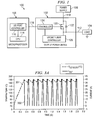
- FIGURE 2 illustrates an example semiconductor device 200 having an integrated PWM current and power limiter according.to one embodiment of this disclosure.
- the semiconductor device 200 could, for example, represent the output power device 102 shown in FIGURE
- the semiconductor device 200 receives two input signals 202a-202b at pins IN1 and IN2.
- the semiconductor device 200 produces two output power signals 204a-204b at pins OUT1 and OUT2.
- the output power signals 204a-204b provide power to one or more loads, such as load 104 of FIGURE 1, coupled to the semiconductor device 200.
- the input signals 202a-202b control whether the semiconductor device 200 produces the output power signals 204a-204b. For example, when the input signal 202a is enabled, an output power signal 204a at pin OUT1 may be produced. Similarly, when the input signal 202b is enabled, an output power signal 204b at pin OUT2 may be produced.
- the input signals 202a-202b could, for example, represent control signals 118 from the microcontroller 106 of FIGURE 1. In this example, the input signals 202a-202b pass through two buffers 206a-206b, which could represent any suitable buffers.
- the semiconductor device 200 includes two switching transistors 208a-208b and two diodes 210a-210b.
- the switching transistors 208a-208b are capable of receiving a supply voltage provided at pin V cc .
- the supply voltage could, for example, represent the voltage signal 110 from the power supply 108 of FIGURE 1.
- the switching transistors 208a-208b are also capable of generating the output power signals 204a-204b.
- each of the switching transistors 208a-208b may be selectively placed in conducting and non-conducting states to generate an output signal having a suitable duty cycle.
- the diodes 210a-210b reduce or prevent inappropriate current flow between the sources and drains of the switching transistors 208a-208b.
- Each of the transistors 208a-208b may represent any suitable transistor or combination of transistors, such as an n-channel MOSFET.
- Each of the diodes 210a-210b may represent any suitable type of diode and number of diodes.
- a logic and control unit 212 controls the operation of the semiconductor device 200.
- the logic and control unit 212 may be coupled to gates of the switching transistors 208a-208b through two drivers 214a-214b.
- the logic and control unit 212 may provide signals to the transistors 208a-208b through the drivers 214a-214b to place each of the transistors 208a-208b in the conducting and non-conducting states as needed. In this way, the logic and control unit 212 causes the transistors. 208a-208b to produce the output power signals 204a-204b having appropriate duty cycles.
- the drivers 214a-214b receive the signals generated by the logic and control unit 212 and.provide control signals to the gates of the transistors 208a-208b.
- the logic and control unit 212 includes any hardware, software, firmware, or combination thereof for controlling the operation of the semiconductor device 200.
- the logic and control unit 212 could, for example, represent the controller 124 of FIGURE 1.
- the drivers 214a-214b represent any hardware, software, firmware, or combination thereof for driving control signals used to control the transistors 208a-208b, such as charge pumps.
- the semiconductor device 100 includes two power clamps 216a-216b.
- the power clamps 216a-216b are coupled to the drivers 214a-214b, the pin V cc , and the gates and drains of the transistors 208a-208b.
- the power clamps 216a-216b ensure that the transistors 208a-208b are not driven by an excessive amount, which could damage the transistors 208a-208b.
- Each of the power clamps 216a-216b represents any hardware, software, firmware, or combination thereof for limiting the power of a signal.
- an input voltage clamp 218 may provide a restoring current whenever the supply voltage at pin V cc varies from an expected or desired voltage.
- a reverse battery protector 220 may help to reduce or prevent damage to the semiconductor device 200 caused by reverse installation of a battery or other power source supplying the voltage at pin V cc , accidental.short circuiting, or other inappropriate operation.
- An under-voltage protector 222 may help to reduce or prevent damage to the semiconductor device 200 caused by a supply voltage at pin V cc that fails to meet a minimum threshold voltage.
- PWM current and power limiting in the semiconductor device 200 are provided by two current limiters 224a-224b, two power limiters 226a-226b, and two selectors 228a-228b.
- the current limiters 224a-224b are coupled to the sources of the transistors 208a-208b.
- the current limiters 224a-224b monitor the amount of current provided by the output power signals 204a-204b.
- the current limiters 224a-224b ensure that the current of each of the output power signals 204a-204b does not exceed a threshold current level.
- the current limiters 224a-224b may generate signals that cause the drivers 214a-214b to reduce the duty cycle of one or both of the output power signals 204a-204b to adjust the current provided by the output power signals 204a-204b as needed. This may help to protect the semiconductor device 200 against various problems, such as short circuits (including shorts directly to ground or a voltage source, and unexpected or abnormal low resistive connections to ground or a voltage source), transients resulting from electrical load dumps, or high power operation under normal conditions.
- Each of the current limiters 224a-224b represents any hardware, software, firmware, or combination thereof for limiting the current.in a signal.
- the power limiters 226a-226b are coupled to the sources of the.transistors 208a-208b.
- the power limiters 226a-226b monitor the amount of power provided by the output power signals 204a-204b.
- the power limiters 226a-226b ensure that the power of each of the output power signals 204a-204b does not exceed a threshold power level, such as 30V.
- the power limiters 226a-226b may generate signals that cause the drivers 214a-214b to reduce the duty cycle of one or both of the output power signals 204a-204b to adjust the power provided by the output power signals 204a-204b as needed.
- Each of the power limiters 226a-226b represents any hardware, software, firmware, or combination thereof for limiting the power in a signal.
- the current limiters 224a-224b and the power limiters 226a-226b could, for example, represent the current/power limit controller 126 of FIGURE 1.
- the selectors 228a-228b select which signal is provided to the drivers 214a-214b for driving the transistors 208a-208b. For example, under normal operation, the selectors 228a-228b may output the signals provided.by the logic and control unit 212. If a current limiter detects that an output power signal is providing excessive current, the appropriate selector.could output the signal provided by the current limiter. Similarly, if a power limiter detects that an output power signal is providing excessive power, the appropriate selector could output the signal provided by the power limiter. The signal provided by the current limiter and power limiter could prevent a load 104 from drawing an excessive current or excessive power from the semiconductor device 200.
- the selectors 228a-228b could be controlled in any suitable manner, such as when control signals from the logic and control unit 212 control that is outputted by the selectors 228a-228b.
- Each of the selectors 228a-228b includes any hardware, software, firmware, or combination thereof for selecting and outputting a signal, such as a multiplexer.
- the semiconductor device 200 produces two other output signals, referred to as current sense output signals 230a-230b, at pins SEN1 and SEN2.
- the current sense output signals 230a-230b are proportional to the output power signals 204a-204b provided at pins OUT1 and OUT2.
- the current sense output signals 230a-230b are produced by two tri-state buffers 232a-232b.
- the tri-state buffers 232a-232b receive two signals I OUT1 and I OUT2 .
- the signals I OUT1 and I OUT2 may represent signals having currents that are equal to the currents of the output power signals 204a-204b, respectively.
- the tri-state buffers 232a-232b also factor the signals I OUT1 and I OUT2 by a value of K and provide the factored signals as the current sense output signals 230a-230b. In this way, the tri-state buffers 232a-232b produce current sense output signals 230a-230b that are proportional to the output power signals 204a-204b.
- the tri-state buffers 232a-232b represent any suitable buffers.
- the tri-state buffers 232a-232b are controlled by a control signal received at pin CS_DIS, which determines whether or not the tri-state buffers 232a-232b output the factored signals I OUT1 and I OUT2 .
- the control signal received at pin CS_DIS may have a low logic level during normal operation, allowing the tri-state buffers 232a-232b to output the factored signals I OUT1 and I OUT2 as the current sense output signals 230a-230b.
- the fault could be indicated by one or more output pins. (as described below), and the tri-state buffers 232a-232b could be placed in a tri-state condition.
- the semiconductor device 200 further includes two fault storage buffers 234a-234b, which are used to produce two additional output signals (referred to as diagnostic output signals 236a-236b) at pins DIAG1 and DIAG2.
- the fault storage buffers 234a-234b store information identifying a fault in the semiconductor device 200. For example, when one or more faults are detected in the semiconductor device 200 (such as excessive temperature), the logic and control unit 212 could generate one or more fault conditions identifying the fault(s).
- the fault storage buffers 234a-234b store the fault conditions produced by the logic and control unit 212. A detected fault condition could then be provided.through the pins DIAG1 and DIAG2 using, for example, a simple analog, digital, or serial digital format.
- the fault storage buffers 234a-234b represent any structure or structures capable of storing information. Also, in other embodiments, the fault conditions stored in the fault storage buffers 234a-234b could be provided through the SEN1 and SEN2 pins.
- the semiconductor device 200 includes one or more temperature sensors 238.
- the temperature sensors 238 measure temperatures or temperature gradients as a function of time and provide reference temperature measurements to the logic and control unit 212. If a reference temperature measurement exceeds a threshold, the logic and control unit 212 could take any appropriate action, such as entering a self-limiting mode.
- a reference temperature measurement could indicate a calculated temperature rise over a short time period that would allow the power limiters 226a-226b to alter the duty cycle of one or both output signals 204a-204b, allowing operation at reduced levels during fast transients or in-rush conditions.
- Each temperature sensor 238 represents any structure capable of measuring a temperature.
- the semiconductor device 200 implements a PWM control scheme using the current limiters.224a-224b and the power limiters 226a-226b. Because the PWM control scheme is implemented in the semiconductor device 200 rather than an external component such as a microcontroller, the number of inputs required by the microcontroller may be reduced. This may help to reduce the size and cost of the microcontroller. Also, the semiconductor device 200 could be used in stand-alone applications where no microcontroller is provided. In the stand-alone applications, the input pins IN1 and/or IN2 could be tied directly to a logic value that activates the semiconductor device 200. Further, the semiconductor device 200 could protect itself against various problems, such as under-voltage conditions or excessive temperatures. In addition, the semiconductor device 200 may operate using the actual temperature of the semiconductor device 200, which may help to reduce or avoid thermal stresses in the semiconductor device 200.
- FIGURE 2 illustrates one example of a semiconductor device 200 having an integrated PWM current and power limiter
- the semiconductor device 200 could include any other or additional I/O pins supporting any other functions in the semiconductor device 200.
- the semiconductor device 200 could generate any suitable number of output power signals, including one signal or more than two signals.
- the semiconductor device 200 could include a power.limiter, a current limiter, or both limiters for each output power signal generated.
- FIGURES 3A through 3C illustrate operation of a semiconductor device with and without an integrated PWM current and power limiter according to one embodiment of this disclosure.
- FIGURES 3A and 3B illustrate how the temperature of a semiconductor device and the current level of an output power signal generated by the semiconductor device may vary over time
- FIGURE 3C illustrates how an output power signal and a current sense output signal vary over time.
- the operations illustrated in FIGURES 3A through 3C are for illustration only. Other embodiments of the semiconductor device that operate in other ways may be used without departing from the scope of this disclosure.
- FIGURE 3A illustrates the operation of a semiconductor device during a permanent overload or short circuit condition without an integrated PWM current and power limiter.
- line 302 represents the current of the output power signal produced by the semiconductor device
- line 304 represents the temperature of the semiconductor device.
- the semiconductor device is suffering from a passive short circuit condition.
- the current (represented by line 302) of the output power signal rapidly oscillates between approximately 0A and approximately 40A.
- the temperature (represented by line 304) of the semiconductor device increases rapidly from approximately 20°C to approximately 180°C. The temperature then oscillates between approximately 180°C and approximately 160°C.
- the current is at or near 0A, the temperature falls gradually.
- the current is at.or near 40A, the temperature increases rapidly.
- the rapid initial increase in temperature and the rapid oscillations in temperature place thermal stress on the semiconductor device, which may damage and shorten the life of the semiconductor device.
- the device would turn off in an over-temperature condition (despite its input) and turn back on when it cools to a lower temperature based on an over-temperature hysterisis limit.
- FIGURE 3B illustrates the operation of a semiconductor device with an integrated PWM current and power limiter, such as the semiconductor device 200 of FIGURE 2.
- line 322 represents the current of the output power signal (such as signal 204a) produced by the semiconductor device 200
- line 324 represents the temperature of the semiconductor device 200.
- the semiconductor device 200 is suffering from a passive short circuit condition.
- the current (represented by line 322) of the output.power signal 204a oscillates between approximately 0A and approximately 20A.
- the temperature (represented by line 324) of the semiconductor device 200 increases from approximately 20°C to approximately 180°C, and the temperature then oscillates between approximately 180°C and approximately 160°C.
- the current oscillates more gradually in FIGURE 3B than in FIGURE 3A.
- the oscillations in current and temperature occur more slowly.
- the oscillation in current occurs later in FIGURE 3B than in FIGURE 3A, and the temperature increases more slowly during this initial period.
- the semiconductor device 200 Because the semiconductor device 200 includes an integrated PWM control scheme, the semiconductor device 200 experiences less thermal stress. The temperature rises more slowly at the start of the short condition and oscillates slower during the short condition. Also, the current oscillates slower and reaches a lower level. This helps to reduce the stress placed on the semiconductor device 200, which may also help to increase the life of the semiconductor device 200.
- FIGURE 3C illustrates the operation of a semiconductor device during an in-rush or fast transient condition with.an integrated PWM current and power limiter, such as the semiconductor device 200 of FIGURE 2.
- line 352 represents the current of the output power.signal (such as signal 204a) produced by the semiconductor device 200
- line 354 represents the current of a current sense output signal (such as signal 230a) produced by the semiconductor device 200.
- the current sense output signal generally follows the output power signal.
- the semiconductor device 200 returns to normal operation after the in-rush or fast transient condition has ended.
- FIGURES 3A through 3C illustrate example operation of a semiconductor device with and without an integrated PWM current and power limiter
- various changes may be made to FIGURES 3A through 3C.
- FIGURES 3A through 3C are provided only as an illustration of possible operation of semiconductor devices with and without an integrated PWM current and power limiter. Further, the temperature and current values and times indicated in FIGURES 3A through 3C are only references, and their actual values may be determined by the final device design parameters.
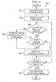
- FIGURE 4 illustrates an example method 400 for PWM current and power limiting in a semiconductor device according to one embodiment of this disclosure.
- the method 400 is described with respect to the semiconductor device 200 of FIGURE 2 operating as the output power device 102 in FIGURE 1.
- the method 400 could be used by any other device and in any other system without departing from the scope of this disclosure.
- the semiconductor device 200 receives an activation signal from an external source at step 402. This may include, for example, the semiconductor device 200 receiving a control signal 118 having a high logic level from a microcontroller 118 as an input signal 202a.
- the semiconductor device 200 generates an output power signal at.step 404.
- This may include, for example, the logic and control unit 212 in the semiconductor device 200 detecting the input signal 202a. This may also include the logic and control unit 212 causing the driver 214a to drive the transistor 208a into conducting and non-conducting states to generate an output power signal 204a having an appropriate duty cycle. This may further include providing the output power signal 204a to a load, such as a load 104.
- the semiconductor device 200 determines whether any current limiting or power limiting problems with the semiconductor device 200 are detected at step 406. This may include, for example, the current limiter 224a and/or the power limiter 226a determining whether too much current or power is being provided by.the output power signal 204a. This may also include the logic and control unit 212 detecting a temperature above a threshold from the temperature sensor 238.
- the semiconductor device 200 enters a self-limiting mode and/or adjusts the output power signal at step 408.
- This may include, for example, the logic and control unit 212, current limiter 224a, or power limiter 226a controlling the transistor 208a so that only a limited amount of current and power may be drawn from the semiconductor device 200..
- This may also include the current limiter 224a or the power limiter 226a.adjusting the duty cycle of the output power signal 204a.
- the semiconductor device 200 could remain in the self-limiting mode for any specified period of time, such as during the time that the fault is detected or until a reset occurs.
- the semiconductor device 200 determines whether any other problems are detected at step 410. This may include, for example, the logic and control unit 212 receiving an indication of an under-voltage condition from the under-voltage sensor 222.
- the semiconductor device 200 After step 408 or if another problem is detected at step 410, the semiconductor device 200 writes a fault condition identifying the detected problem at step 412. This may include, for example, the logic and control unit 212 writing the fault condition to the fault storage buffer 228a.
- the semiconductor device 200 determines whether a. deactivation signal from an external source is received at step 414. This may include, for example, the semiconductor device 200 receiving a control signal 118 having a low logic level from the microcontroller 118 as an input signal 202a.
- the semiconductor device 200 If no deactivation signal is detected, the semiconductor device 200 returns to step 406. Otherwise, the semiconductor device 200 stops generating the output power signal at step 416. This may include, for example, the logic and control unit 212 in the semiconductor device 200 detecting the input signal 202a. This may also include the logic and control unit 212 causing the driver 214a to drive the transistor 208a into the non-conducting state. At this point, no more power is provided to the load 104 coupled to the semiconductor device 200.
- FIGURE 4 illustrates one example of a method 400 for PWM current and power limiting in a semiconductor device
- various changes may be made to FIGURE 4.
- the semiconductor device 200 could generate the output power signal at step 404 and determine whether problems are detected at step 408 in parallel.
- the activation and deactivation signals are shown as originating at a microcontroller, the activation signal and/or deactivation signal could originate from other sources.
- the IN1 pin of the semiconductor device 200 could be tied to a logic level that activates the semiconductor device 200. In this case, the semiconductor device 200 still receives an activation signal, and the signal remains constant as long as power is supplied to the system 100.
- the semiconductor device 200 may support only one of power limiting and current limiting.
- controller and "microcontroller” mean any device, system, or part thereof that controls at least one operation.
- a controller.. or microcontroller may be implemented in hardware, firmware, or software, or a combination of at least.two of the same. It should be noted that the functionality associated with any particular controller or microcontroller may be centralized or distributed, whether locally or remotely.'
Landscapes
- Engineering & Computer Science (AREA)
- Power Engineering (AREA)
- Dc-Dc Converters (AREA)
Applications Claiming Priority (1)
| Application Number | Priority Date | Filing Date | Title |
|---|---|---|---|
| US11/172,515 US20070013361A1 (en) | 2005-06-30 | 2005-06-30 | Semiconductor device having an integrated, self-regulated PWM current and power limiter and method |
Publications (3)
| Publication Number | Publication Date |
|---|---|
| EP1739833A2 true EP1739833A2 (de) | 2007-01-03 |
| EP1739833A3 EP1739833A3 (de) | 2009-11-04 |
| EP1739833B1 EP1739833B1 (de) | 2015-11-11 |
Family
ID=37056178
Family Applications (1)
| Application Number | Title | Priority Date | Filing Date |
|---|---|---|---|
| EP06253188.4A Active EP1739833B1 (de) | 2005-06-30 | 2006-06-20 | Halbleitervorrichtung mit integriertem selbstreguliertem PWM-Strom, Leistungsbegrenzer und Verfahren |
Country Status (2)
| Country | Link |
|---|---|
| US (2) | US20070013361A1 (de) |
| EP (1) | EP1739833B1 (de) |
Cited By (3)
| Publication number | Priority date | Publication date | Assignee | Title |
|---|---|---|---|---|
| EP1925194A2 (de) * | 2005-09-14 | 2008-05-28 | Siemens Aktiengesellschaft Österreich | Verfahren zum betreiben von schaltnetzteilen |
| CN102037647A (zh) * | 2008-05-21 | 2011-04-27 | 三垦电气株式会社 | 高边驱动器 |
| EP3696979A1 (de) * | 2019-02-15 | 2020-08-19 | Siemens Aktiengesellschaft | Elektronischer schalter mit stromregulierung |
Families Citing this family (19)
| Publication number | Priority date | Publication date | Assignee | Title |
|---|---|---|---|---|
| US20070069521A1 (en) * | 2005-09-23 | 2007-03-29 | C.E. Niehoff & Co. | Power control system and method |
| JP5426102B2 (ja) * | 2007-02-28 | 2014-02-26 | エスティーマイクロエレクトロニクス,インコーポレイテッド | 車両のバッテリチャージを保存し且つトレーラー負荷を保護する集積回路及び方法 |
| CN102395937B (zh) * | 2009-04-17 | 2014-06-11 | 惠普开发有限公司 | 功率封顶系统及方法 |
| US8810058B2 (en) * | 2010-06-01 | 2014-08-19 | Enerdel, Inc. | Multi-use input |
| US8947064B2 (en) * | 2011-09-20 | 2015-02-03 | Infineon Technologies Austria Ag | System and method for driving an electronic switch dependent on temperature |
| US9272659B1 (en) * | 2011-11-04 | 2016-03-01 | Marcus C. Boykin | Auxiliary vehicle lamp operation system |
| ITMI20130001A1 (it) * | 2013-01-03 | 2014-07-04 | St Microelectronics Srl | SISTEMA ELETTRICO COMPRENDENTE UN APPARATO DI PILOTAGGIO DI UN CARICO CON AUTO-RIAVVIO E METODO DI FUNZIONAMENTO DELLÂeuro¿APPARATO |
| US9591713B2 (en) * | 2013-06-25 | 2017-03-07 | Lumastream Canada Ulc | Apparatus and method for monitoring and limiting power to SSL devices |
| US10247793B2 (en) * | 2014-03-31 | 2019-04-02 | Koninklijke Philips N.V. | Receive coils with low-loss detune circuits for magnetic resonance (MR) systems and method of operation thereof |
| US9625499B2 (en) * | 2014-05-01 | 2017-04-18 | Eaton Corporation | Receptacle indicating relative level of current or energy |
| JP6256292B2 (ja) * | 2014-10-22 | 2018-01-10 | 株式会社デンソー | 温度保護装置 |
| WO2016068194A1 (ja) * | 2014-10-30 | 2016-05-06 | 矢崎総業株式会社 | 車両用電源制御装置 |
| JP6539100B2 (ja) * | 2015-04-27 | 2019-07-03 | 矢崎総業株式会社 | 車両用電源制御装置 |
| US9780640B2 (en) * | 2015-12-15 | 2017-10-03 | Monolithic Power Systems, Inc. | Multi-phase voltage converter with fault instruction circuit |
| JP6965537B2 (ja) * | 2017-03-16 | 2021-11-10 | 富士電機株式会社 | 半導体素子の駆動装置 |
| US10833656B2 (en) * | 2018-04-30 | 2020-11-10 | Micron Technology, Inc. | Autonomous duty cycle calibration |
| JP7314103B2 (ja) * | 2020-07-17 | 2023-07-25 | 日立グローバルライフソリューションズ株式会社 | 電動機の制御装置 |
| DE102020133306B4 (de) | 2020-12-14 | 2023-08-10 | Dr. Ing. H.C. F. Porsche Aktiengesellschaft | Verfahren zur Steuerung einer Ladeeinrichtung |
| US11626870B1 (en) * | 2022-01-11 | 2023-04-11 | Infineon Technologies Austria Ag | Gate driver |
Citations (2)
| Publication number | Priority date | Publication date | Assignee | Title |
|---|---|---|---|---|
| US5293077A (en) | 1988-02-29 | 1994-03-08 | Hitachi, Ltd. | Power switching circuit |
| EP1357461A2 (de) | 2002-04-19 | 2003-10-29 | Daimlerchrysler Corporation | Programmierbarer Stromsteuerungsschalter |
Family Cites Families (11)
| Publication number | Priority date | Publication date | Assignee | Title |
|---|---|---|---|---|
| US4845419A (en) * | 1985-11-12 | 1989-07-04 | Norand Corporation | Automatic control means providing a low-power responsive signal, particularly for initiating data preservation operation |
| US4924112A (en) * | 1988-10-31 | 1990-05-08 | Motorola Inc. | Microprocessor having high current drive and feedback for temperature control |
| JP3430773B2 (ja) * | 1996-02-21 | 2003-07-28 | 株式会社明電舎 | インバータ装置におけるスイッチング素子の過熱保護方法 |
| JP3695023B2 (ja) * | 1996-11-27 | 2005-09-14 | 日産自動車株式会社 | 電気自動車の過負荷防止装置 |
| US6060792A (en) * | 1997-05-20 | 2000-05-09 | International Rectifier Corp. | Instantaneous junction temperature detection |
| US7035064B2 (en) * | 1998-05-29 | 2006-04-25 | Semikron Elektronik Gmbh | Method and circuit arrangement with adaptive overload protection for power switching devices |
| US6144187A (en) * | 1998-11-12 | 2000-11-07 | Fairchild Semiconductor Corporation | Power measurement for adaptive battery charger |
| US6118254A (en) * | 1999-07-30 | 2000-09-12 | Compaq Computer Corporation | Battery charge control architecture for constant voltage maximum power operation |
| US6934139B2 (en) * | 2000-05-01 | 2005-08-23 | Fuji Electric Device Technology Co., Ltd. | Intelligent power module |
| JP2004208450A (ja) * | 2002-12-26 | 2004-07-22 | Sanden Corp | モータ制御装置 |
| US6972969B1 (en) * | 2004-08-19 | 2005-12-06 | Iwatt, Inc. | System and method for controlling current limit with primary side sensing |
-
2005
- 2005-06-30 US US11/172,515 patent/US20070013361A1/en not_active Abandoned
-
2006
- 2006-06-20 EP EP06253188.4A patent/EP1739833B1/de active Active
-
2008
- 2008-02-20 US US12/070,710 patent/US7671571B2/en not_active Expired - Lifetime
Patent Citations (2)
| Publication number | Priority date | Publication date | Assignee | Title |
|---|---|---|---|---|
| US5293077A (en) | 1988-02-29 | 1994-03-08 | Hitachi, Ltd. | Power switching circuit |
| EP1357461A2 (de) | 2002-04-19 | 2003-10-29 | Daimlerchrysler Corporation | Programmierbarer Stromsteuerungsschalter |
Cited By (9)
| Publication number | Priority date | Publication date | Assignee | Title |
|---|---|---|---|---|
| EP1925194A2 (de) * | 2005-09-14 | 2008-05-28 | Siemens Aktiengesellschaft Österreich | Verfahren zum betreiben von schaltnetzteilen |
| US8212434B2 (en) | 2005-09-14 | 2012-07-03 | Siemens Aktiengesellschaft | Method for operating switched-mode power supply units |
| CN102037647A (zh) * | 2008-05-21 | 2011-04-27 | 三垦电气株式会社 | 高边驱动器 |
| EP2302795A4 (de) * | 2008-05-21 | 2011-07-20 | Sanken Electric Co Ltd | High-side-treiber |
| US8169765B2 (en) | 2008-05-21 | 2012-05-01 | Sanken Electric Co., Ltd. | High-side driver |
| CN102037647B (zh) * | 2008-05-21 | 2013-05-15 | 三垦电气株式会社 | 高边驱动器 |
| EP3696979A1 (de) * | 2019-02-15 | 2020-08-19 | Siemens Aktiengesellschaft | Elektronischer schalter mit stromregulierung |
| WO2020165215A1 (de) * | 2019-02-15 | 2020-08-20 | Siemens Aktiengesellschaft | Elektronischer schalter mit stromregulierung |
| US11509301B2 (en) | 2019-02-15 | 2022-11-22 | Siemens Aktiengesellschaft | Electronic switch with current regulation |
Also Published As
| Publication number | Publication date |
|---|---|
| US20070013361A1 (en) | 2007-01-18 |
| EP1739833A3 (de) | 2009-11-04 |
| US7671571B2 (en) | 2010-03-02 |
| US20080284404A1 (en) | 2008-11-20 |
| EP1739833B1 (de) | 2015-11-11 |
Similar Documents
| Publication | Publication Date | Title |
|---|---|---|
| US7671571B2 (en) | Semiconductor device having an integrated, self-regulated PWM current and power limiter and method | |
| US8054605B2 (en) | Power supply controller | |
| US7741820B2 (en) | Switching voltage regulator pulse width modulation controller and method | |
| US8633755B2 (en) | Load driver with constant current variable structure | |
| US7345383B2 (en) | Abnormality detection apparatus for a power feed circuit | |
| KR100715567B1 (ko) | 반도체 스위치의 제어장치 | |
| US8254075B2 (en) | Semiconductor device and circuit protection method | |
| US8598859B2 (en) | Power supply controller | |
| EP2110935A2 (de) | Gleichstromwandler | |
| US8760832B2 (en) | Load circuit protection device | |
| US20040070910A1 (en) | Method for driving a semiconductor switch and circuit configuration with a semiconductor switch | |
| US20170214313A1 (en) | Drive circuit for semiconductor switching element | |
| US5920452A (en) | Circuit and method for protecting from overcurrent conditions and detecting an open electrical load | |
| US11133667B2 (en) | Protection circuit, corresponding system and method | |
| US12266922B2 (en) | Reverse battery protection circuit with isolation and reverse polarity circuits | |
| US6728084B2 (en) | System and method for overvoltage protection of an integrated circuit | |
| US7477502B1 (en) | Method and system for providing fault protection in a power supply system | |
| US20180062376A1 (en) | An electronic fuse circuit, corresponding device and method | |
| US12614902B2 (en) | Intelligent semiconductor switch | |
| CN110166032A (zh) | 使用脉冲操作对栅极驱动器进行短路保护 | |
| WO2015016885A1 (en) | Digital pulse width modulation control for load switch circuits | |
| KR100689328B1 (ko) | 인버터 보호 장치 | |
| KR102046350B1 (ko) | 승객 보호 수단을 위한 집적 조정기, 특히 전압 조정기 및 제어 장치 | |
| KR20010084792A (ko) | 아이피엠(ipm) 보호회로 | |
| US12048076B2 (en) | System and method for inrush current control with combinational load drive configuration |
Legal Events
| Date | Code | Title | Description |
|---|---|---|---|
| PUAI | Public reference made under article 153(3) epc to a published international application that has entered the european phase |
Free format text: ORIGINAL CODE: 0009012 |
|
| AK | Designated contracting states |
Kind code of ref document: A2 Designated state(s): AT BE BG CH CY CZ DE DK EE ES FI FR GB GR HU IE IS IT LI LT LU LV MC NL PL PT RO SE SI SK TR |
|
| AX | Request for extension of the european patent |
Extension state: AL BA HR MK YU |
|
| PUAL | Search report despatched |
Free format text: ORIGINAL CODE: 0009013 |
|
| AK | Designated contracting states |
Kind code of ref document: A3 Designated state(s): AT BE BG CH CY CZ DE DK EE ES FI FR GB GR HU IE IS IT LI LT LU LV MC NL PL PT RO SE SI SK TR |
|
| AX | Request for extension of the european patent |
Extension state: AL BA HR MK RS |
|
| RIC1 | Information provided on ipc code assigned before grant |
Ipc: H03K 7/08 20060101AFI20061012BHEP Ipc: H03K 17/082 20060101ALI20090925BHEP Ipc: H03K 17/18 20060101ALI20090925BHEP |
|
| 17P | Request for examination filed |
Effective date: 20100427 |
|
| AKX | Designation fees paid |
Designated state(s): DE FR GB IT |
|
| 17Q | First examination report despatched |
Effective date: 20100615 |
|
| RAP1 | Party data changed (applicant data changed or rights of an application transferred) |
Owner name: STMICROELECTRONICS, INC. |
|
| GRAP | Despatch of communication of intention to grant a patent |
Free format text: ORIGINAL CODE: EPIDOSNIGR1 |
|
| INTG | Intention to grant announced |
Effective date: 20150203 |
|
| GRAP | Despatch of communication of intention to grant a patent |
Free format text: ORIGINAL CODE: EPIDOSNIGR1 |
|
| INTG | Intention to grant announced |
Effective date: 20150608 |
|
| GRAS | Grant fee paid |
Free format text: ORIGINAL CODE: EPIDOSNIGR3 |
|
| GRAA | (expected) grant |
Free format text: ORIGINAL CODE: 0009210 |
|
| AK | Designated contracting states |
Kind code of ref document: B1 Designated state(s): DE FR GB IT |
|
| REG | Reference to a national code |
Ref country code: GB Ref legal event code: FG4D |
|
| REG | Reference to a national code |
Ref country code: DE Ref legal event code: R096 Ref document number: 602006047216 Country of ref document: DE |
|
| PG25 | Lapsed in a contracting state [announced via postgrant information from national office to epo] |
Ref country code: IT Free format text: LAPSE BECAUSE OF FAILURE TO SUBMIT A TRANSLATION OF THE DESCRIPTION OR TO PAY THE FEE WITHIN THE PRESCRIBED TIME-LIMIT Effective date: 20151111 |
|
| REG | Reference to a national code |
Ref country code: DE Ref legal event code: R097 Ref document number: 602006047216 Country of ref document: DE |
|
| PLBE | No opposition filed within time limit |
Free format text: ORIGINAL CODE: 0009261 |
|
| STAA | Information on the status of an ep patent application or granted ep patent |
Free format text: STATUS: NO OPPOSITION FILED WITHIN TIME LIMIT |
|
| 26N | No opposition filed |
Effective date: 20160812 |
|
| GBPC | Gb: european patent ceased through non-payment of renewal fee |
Effective date: 20160620 |
|
| REG | Reference to a national code |
Ref country code: FR Ref legal event code: ST Effective date: 20170228 |
|
| PG25 | Lapsed in a contracting state [announced via postgrant information from national office to epo] |
Ref country code: FR Free format text: LAPSE BECAUSE OF NON-PAYMENT OF DUE FEES Effective date: 20160630 |
|
| PG25 | Lapsed in a contracting state [announced via postgrant information from national office to epo] |
Ref country code: GB Free format text: LAPSE BECAUSE OF NON-PAYMENT OF DUE FEES Effective date: 20160620 |
|
| REG | Reference to a national code |
Ref country code: DE Ref legal event code: R082 Ref document number: 602006047216 Country of ref document: DE Representative=s name: PAGE, WHITE & FARRER GERMANY LLP, DE |
|
| P01 | Opt-out of the competence of the unified patent court (upc) registered |
Effective date: 20230521 |
|
| PGFP | Annual fee paid to national office [announced via postgrant information from national office to epo] |
Ref country code: DE Payment date: 20250520 Year of fee payment: 20 |