EP1740025A2 - Leiterplatte und Verfahren zu deren Herstellung - Google Patents
Leiterplatte und Verfahren zu deren Herstellung Download PDFInfo
- Publication number
- EP1740025A2 EP1740025A2 EP06011507A EP06011507A EP1740025A2 EP 1740025 A2 EP1740025 A2 EP 1740025A2 EP 06011507 A EP06011507 A EP 06011507A EP 06011507 A EP06011507 A EP 06011507A EP 1740025 A2 EP1740025 A2 EP 1740025A2
- Authority
- EP
- European Patent Office
- Prior art keywords
- wiring board
- layer
- reinforcing
- insulating layer
- wiring
- Prior art date
- Legal status (The legal status is an assumption and is not a legal conclusion. Google has not performed a legal analysis and makes no representation as to the accuracy of the status listed.)
- Granted
Links
Images












Classifications
-
- H—ELECTRICITY
- H05—ELECTRIC TECHNIQUES NOT OTHERWISE PROVIDED FOR
- H05K—PRINTED CIRCUITS; CASINGS OR CONSTRUCTIONAL DETAILS OF ELECTRIC APPARATUS; MANUFACTURE OF ASSEMBLAGES OF ELECTRICAL COMPONENTS
- H05K1/00—Printed circuits
- H05K1/18—Printed circuits structurally associated with non-printed electric components
- H05K1/182—Printed circuits structurally associated with non-printed electric components associated with components mounted in printed circuit boards [PCB], e.g. insert-mounted components [IMC]
- H05K1/185—Printed circuits structurally associated with non-printed electric components associated with components mounted in printed circuit boards [PCB], e.g. insert-mounted components [IMC] associated with components encapsulated in the insulating substrate of the PCBs; associated with components incorporated in internal layers of multilayer circuit boards
- H05K1/186—Printed circuits structurally associated with non-printed electric components associated with components mounted in printed circuit boards [PCB], e.g. insert-mounted components [IMC] associated with components encapsulated in the insulating substrate of the PCBs; associated with components incorporated in internal layers of multilayer circuit boards manufactured by mounting on or connecting to patterned circuits before or during embedding
-
- H—ELECTRICITY
- H05—ELECTRIC TECHNIQUES NOT OTHERWISE PROVIDED FOR
- H05K—PRINTED CIRCUITS; CASINGS OR CONSTRUCTIONAL DETAILS OF ELECTRIC APPARATUS; MANUFACTURE OF ASSEMBLAGES OF ELECTRICAL COMPONENTS
- H05K3/00—Apparatus or processes for manufacturing printed circuits
- H05K3/46—Manufacturing multilayer circuits
-
- H—ELECTRICITY
- H10—SEMICONDUCTOR DEVICES; ELECTRIC SOLID-STATE DEVICES NOT OTHERWISE PROVIDED FOR
- H10W—GENERIC PACKAGES, INTERCONNECTIONS, CONNECTORS OR OTHER CONSTRUCTIONAL DETAILS OF DEVICES COVERED BY CLASS H10
- H10W40/00—Arrangements for thermal protection or thermal control
- H10W40/20—Arrangements for cooling
- H10W40/22—Arrangements for cooling characterised by their shape, e.g. having conical or cylindrical projections
- H10W40/226—Arrangements for cooling characterised by their shape, e.g. having conical or cylindrical projections characterised by projecting parts, e.g. fins to increase surface area
- H10W40/228—Arrangements for cooling characterised by their shape, e.g. having conical or cylindrical projections characterised by projecting parts, e.g. fins to increase surface area the projecting parts being wire-shaped or pin-shaped
-
- H—ELECTRICITY
- H10—SEMICONDUCTOR DEVICES; ELECTRIC SOLID-STATE DEVICES NOT OTHERWISE PROVIDED FOR
- H10W—GENERIC PACKAGES, INTERCONNECTIONS, CONNECTORS OR OTHER CONSTRUCTIONAL DETAILS OF DEVICES COVERED BY CLASS H10
- H10W70/00—Package substrates; Interposers; Redistribution layers [RDL]
- H10W70/01—Manufacture or treatment
- H10W70/05—Manufacture or treatment of insulating or insulated package substrates, or of interposers, or of redistribution layers
- H10W70/08—Manufacture or treatment of insulating or insulated package substrates, or of interposers, or of redistribution layers by depositing layers on the chip or wafer, e.g. "chip-first" RDLs
- H10W70/09—Manufacture or treatment of insulating or insulated package substrates, or of interposers, or of redistribution layers by depositing layers on the chip or wafer, e.g. "chip-first" RDLs extending onto an encapsulation that laterally surrounds the chip or wafer, e.g. fan-out wafer level package [FOWLP] RDLs
-
- H—ELECTRICITY
- H10—SEMICONDUCTOR DEVICES; ELECTRIC SOLID-STATE DEVICES NOT OTHERWISE PROVIDED FOR
- H10W—GENERIC PACKAGES, INTERCONNECTIONS, CONNECTORS OR OTHER CONSTRUCTIONAL DETAILS OF DEVICES COVERED BY CLASS H10
- H10W70/00—Package substrates; Interposers; Redistribution layers [RDL]
- H10W70/60—Insulating or insulated package substrates; Interposers; Redistribution layers
- H10W70/611—Insulating or insulated package substrates; Interposers; Redistribution layers for connecting multiple chips together
- H10W70/614—Insulating or insulated package substrates; Interposers; Redistribution layers for connecting multiple chips together the multiple chips being integrally enclosed
-
- H—ELECTRICITY
- H10—SEMICONDUCTOR DEVICES; ELECTRIC SOLID-STATE DEVICES NOT OTHERWISE PROVIDED FOR
- H10W—GENERIC PACKAGES, INTERCONNECTIONS, CONNECTORS OR OTHER CONSTRUCTIONAL DETAILS OF DEVICES COVERED BY CLASS H10
- H10W90/00—Package configurations
-
- H—ELECTRICITY
- H05—ELECTRIC TECHNIQUES NOT OTHERWISE PROVIDED FOR
- H05K—PRINTED CIRCUITS; CASINGS OR CONSTRUCTIONAL DETAILS OF ELECTRIC APPARATUS; MANUFACTURE OF ASSEMBLAGES OF ELECTRICAL COMPONENTS
- H05K1/00—Printed circuits
- H05K1/02—Details
- H05K1/0271—Arrangements for reducing stress or warp in rigid printed circuit boards, e.g. caused by loads, vibrations or differences in thermal expansion
-
- H—ELECTRICITY
- H05—ELECTRIC TECHNIQUES NOT OTHERWISE PROVIDED FOR
- H05K—PRINTED CIRCUITS; CASINGS OR CONSTRUCTIONAL DETAILS OF ELECTRIC APPARATUS; MANUFACTURE OF ASSEMBLAGES OF ELECTRICAL COMPONENTS
- H05K3/00—Apparatus or processes for manufacturing printed circuits
- H05K3/10—Apparatus or processes for manufacturing printed circuits in which conductive material is applied to the insulating support in such a manner as to form the desired conductive pattern
- H05K3/20—Apparatus or processes for manufacturing printed circuits in which conductive material is applied to the insulating support in such a manner as to form the desired conductive pattern by affixing prefabricated conductor pattern
-
- H—ELECTRICITY
- H05—ELECTRIC TECHNIQUES NOT OTHERWISE PROVIDED FOR
- H05K—PRINTED CIRCUITS; CASINGS OR CONSTRUCTIONAL DETAILS OF ELECTRIC APPARATUS; MANUFACTURE OF ASSEMBLAGES OF ELECTRICAL COMPONENTS
- H05K3/00—Apparatus or processes for manufacturing printed circuits
- H05K3/46—Manufacturing multilayer circuits
- H05K3/4644—Manufacturing multilayer circuits by building the multilayer layer by layer, i.e. build-up multilayer circuits
-
- H—ELECTRICITY
- H05—ELECTRIC TECHNIQUES NOT OTHERWISE PROVIDED FOR
- H05K—PRINTED CIRCUITS; CASINGS OR CONSTRUCTIONAL DETAILS OF ELECTRIC APPARATUS; MANUFACTURE OF ASSEMBLAGES OF ELECTRICAL COMPONENTS
- H05K3/00—Apparatus or processes for manufacturing printed circuits
- H05K3/46—Manufacturing multilayer circuits
- H05K3/4688—Composite multilayer circuits, i.e. comprising insulating layers having different properties
-
- H—ELECTRICITY
- H10—SEMICONDUCTOR DEVICES; ELECTRIC SOLID-STATE DEVICES NOT OTHERWISE PROVIDED FOR
- H10P—GENERIC PROCESSES OR APPARATUS FOR THE MANUFACTURE OR TREATMENT OF DEVICES COVERED BY CLASS H10
- H10P72/00—Handling or holding of wafers, substrates or devices during manufacture or treatment thereof
- H10P72/70—Handling or holding of wafers, substrates or devices during manufacture or treatment thereof for supporting or gripping
- H10P72/74—Handling or holding of wafers, substrates or devices during manufacture or treatment thereof for supporting or gripping using temporarily an auxiliary support
- H10P72/7424—Handling or holding of wafers, substrates or devices during manufacture or treatment thereof for supporting or gripping using temporarily an auxiliary support used as a support during the manufacture of self-supporting substrates
-
- H—ELECTRICITY
- H10—SEMICONDUCTOR DEVICES; ELECTRIC SOLID-STATE DEVICES NOT OTHERWISE PROVIDED FOR
- H10W—GENERIC PACKAGES, INTERCONNECTIONS, CONNECTORS OR OTHER CONSTRUCTIONAL DETAILS OF DEVICES COVERED BY CLASS H10
- H10W70/00—Package substrates; Interposers; Redistribution layers [RDL]
- H10W70/01—Manufacture or treatment
- H10W70/05—Manufacture or treatment of insulating or insulated package substrates, or of interposers, or of redistribution layers
- H10W70/093—Connecting or disconnecting other interconnections thereto or therefrom, e.g. connecting bond wires or bumps
-
- H—ELECTRICITY
- H10—SEMICONDUCTOR DEVICES; ELECTRIC SOLID-STATE DEVICES NOT OTHERWISE PROVIDED FOR
- H10W—GENERIC PACKAGES, INTERCONNECTIONS, CONNECTORS OR OTHER CONSTRUCTIONAL DETAILS OF DEVICES COVERED BY CLASS H10
- H10W70/00—Package substrates; Interposers; Redistribution layers [RDL]
- H10W70/60—Insulating or insulated package substrates; Interposers; Redistribution layers
-
- H—ELECTRICITY
- H10—SEMICONDUCTOR DEVICES; ELECTRIC SOLID-STATE DEVICES NOT OTHERWISE PROVIDED FOR
- H10W—GENERIC PACKAGES, INTERCONNECTIONS, CONNECTORS OR OTHER CONSTRUCTIONAL DETAILS OF DEVICES COVERED BY CLASS H10
- H10W72/00—Interconnections or connectors in packages
- H10W72/071—Connecting or disconnecting
- H10W72/072—Connecting or disconnecting of bump connectors
- H10W72/07202—Connecting or disconnecting of bump connectors using auxiliary members
- H10W72/07204—Connecting or disconnecting of bump connectors using auxiliary members using temporary auxiliary members, e.g. sacrificial coatings
- H10W72/07207—Temporary substrates, e.g. removable substrates
-
- H—ELECTRICITY
- H10—SEMICONDUCTOR DEVICES; ELECTRIC SOLID-STATE DEVICES NOT OTHERWISE PROVIDED FOR
- H10W—GENERIC PACKAGES, INTERCONNECTIONS, CONNECTORS OR OTHER CONSTRUCTIONAL DETAILS OF DEVICES COVERED BY CLASS H10
- H10W72/00—Interconnections or connectors in packages
- H10W72/071—Connecting or disconnecting
- H10W72/073—Connecting or disconnecting of die-attach connectors
- H10W72/07302—Connecting or disconnecting of die-attach connectors using an auxiliary member
- H10W72/07304—Connecting or disconnecting of die-attach connectors using an auxiliary member the auxiliary member being temporary, e.g. a sacrificial coating
- H10W72/07307—Connecting or disconnecting of die-attach connectors using an auxiliary member the auxiliary member being temporary, e.g. a sacrificial coating the auxiliary member being a temporary substrate, e.g. a removable substrate
-
- H—ELECTRICITY
- H10—SEMICONDUCTOR DEVICES; ELECTRIC SOLID-STATE DEVICES NOT OTHERWISE PROVIDED FOR
- H10W—GENERIC PACKAGES, INTERCONNECTIONS, CONNECTORS OR OTHER CONSTRUCTIONAL DETAILS OF DEVICES COVERED BY CLASS H10
- H10W72/00—Interconnections or connectors in packages
- H10W72/851—Dispositions of multiple connectors or interconnections
- H10W72/874—On different surfaces
-
- H—ELECTRICITY
- H10—SEMICONDUCTOR DEVICES; ELECTRIC SOLID-STATE DEVICES NOT OTHERWISE PROVIDED FOR
- H10W—GENERIC PACKAGES, INTERCONNECTIONS, CONNECTORS OR OTHER CONSTRUCTIONAL DETAILS OF DEVICES COVERED BY CLASS H10
- H10W72/00—Interconnections or connectors in packages
- H10W72/851—Dispositions of multiple connectors or interconnections
- H10W72/874—On different surfaces
- H10W72/877—Bump connectors and die-attach connectors
-
- H—ELECTRICITY
- H10—SEMICONDUCTOR DEVICES; ELECTRIC SOLID-STATE DEVICES NOT OTHERWISE PROVIDED FOR
- H10W—GENERIC PACKAGES, INTERCONNECTIONS, CONNECTORS OR OTHER CONSTRUCTIONAL DETAILS OF DEVICES COVERED BY CLASS H10
- H10W72/00—Interconnections or connectors in packages
- H10W72/90—Bond pads, in general
- H10W72/941—Dispositions of bond pads
- H10W72/9413—Dispositions of bond pads on encapsulations
-
- H—ELECTRICITY
- H10—SEMICONDUCTOR DEVICES; ELECTRIC SOLID-STATE DEVICES NOT OTHERWISE PROVIDED FOR
- H10W—GENERIC PACKAGES, INTERCONNECTIONS, CONNECTORS OR OTHER CONSTRUCTIONAL DETAILS OF DEVICES COVERED BY CLASS H10
- H10W74/00—Encapsulations, e.g. protective coatings
-
- H—ELECTRICITY
- H10—SEMICONDUCTOR DEVICES; ELECTRIC SOLID-STATE DEVICES NOT OTHERWISE PROVIDED FOR
- H10W—GENERIC PACKAGES, INTERCONNECTIONS, CONNECTORS OR OTHER CONSTRUCTIONAL DETAILS OF DEVICES COVERED BY CLASS H10
- H10W74/00—Encapsulations, e.g. protective coatings
- H10W74/01—Manufacture or treatment
- H10W74/019—Manufacture or treatment using temporary auxiliary substrates
-
- H—ELECTRICITY
- H10—SEMICONDUCTOR DEVICES; ELECTRIC SOLID-STATE DEVICES NOT OTHERWISE PROVIDED FOR
- H10W—GENERIC PACKAGES, INTERCONNECTIONS, CONNECTORS OR OTHER CONSTRUCTIONAL DETAILS OF DEVICES COVERED BY CLASS H10
- H10W74/00—Encapsulations, e.g. protective coatings
- H10W74/10—Encapsulations, e.g. protective coatings characterised by their shape or disposition
- H10W74/15—Encapsulations, e.g. protective coatings characterised by their shape or disposition on active surfaces of flip-chip devices, e.g. underfills
-
- H—ELECTRICITY
- H10—SEMICONDUCTOR DEVICES; ELECTRIC SOLID-STATE DEVICES NOT OTHERWISE PROVIDED FOR
- H10W—GENERIC PACKAGES, INTERCONNECTIONS, CONNECTORS OR OTHER CONSTRUCTIONAL DETAILS OF DEVICES COVERED BY CLASS H10
- H10W90/00—Package configurations
- H10W90/701—Package configurations characterised by the relative positions of pads or connectors relative to package parts
- H10W90/721—Package configurations characterised by the relative positions of pads or connectors relative to package parts of bump connectors
- H10W90/722—Package configurations characterised by the relative positions of pads or connectors relative to package parts of bump connectors between stacked chips
-
- H—ELECTRICITY
- H10—SEMICONDUCTOR DEVICES; ELECTRIC SOLID-STATE DEVICES NOT OTHERWISE PROVIDED FOR
- H10W—GENERIC PACKAGES, INTERCONNECTIONS, CONNECTORS OR OTHER CONSTRUCTIONAL DETAILS OF DEVICES COVERED BY CLASS H10
- H10W90/00—Package configurations
- H10W90/701—Package configurations characterised by the relative positions of pads or connectors relative to package parts
- H10W90/721—Package configurations characterised by the relative positions of pads or connectors relative to package parts of bump connectors
- H10W90/724—Package configurations characterised by the relative positions of pads or connectors relative to package parts of bump connectors between a chip and a stacked insulating package substrate, interposer or RDL
-
- H—ELECTRICITY
- H10—SEMICONDUCTOR DEVICES; ELECTRIC SOLID-STATE DEVICES NOT OTHERWISE PROVIDED FOR
- H10W—GENERIC PACKAGES, INTERCONNECTIONS, CONNECTORS OR OTHER CONSTRUCTIONAL DETAILS OF DEVICES COVERED BY CLASS H10
- H10W90/00—Package configurations
- H10W90/701—Package configurations characterised by the relative positions of pads or connectors relative to package parts
- H10W90/731—Package configurations characterised by the relative positions of pads or connectors relative to package parts of die-attach connectors
- H10W90/734—Package configurations characterised by the relative positions of pads or connectors relative to package parts of die-attach connectors between a chip and a stacked insulating package substrate, interposer or RDL
-
- Y—GENERAL TAGGING OF NEW TECHNOLOGICAL DEVELOPMENTS; GENERAL TAGGING OF CROSS-SECTIONAL TECHNOLOGIES SPANNING OVER SEVERAL SECTIONS OF THE IPC; TECHNICAL SUBJECTS COVERED BY FORMER USPC CROSS-REFERENCE ART COLLECTIONS [XRACs] AND DIGESTS
- Y10—TECHNICAL SUBJECTS COVERED BY FORMER USPC
- Y10T—TECHNICAL SUBJECTS COVERED BY FORMER US CLASSIFICATION
- Y10T29/00—Metal working
- Y10T29/49—Method of mechanical manufacture
- Y10T29/49002—Electrical device making
- Y10T29/49117—Conductor or circuit manufacturing
- Y10T29/49124—On flat or curved insulated base, e.g., printed circuit, etc.
- Y10T29/49126—Assembling bases
-
- Y—GENERAL TAGGING OF NEW TECHNOLOGICAL DEVELOPMENTS; GENERAL TAGGING OF CROSS-SECTIONAL TECHNOLOGIES SPANNING OVER SEVERAL SECTIONS OF THE IPC; TECHNICAL SUBJECTS COVERED BY FORMER USPC CROSS-REFERENCE ART COLLECTIONS [XRACs] AND DIGESTS
- Y10—TECHNICAL SUBJECTS COVERED BY FORMER USPC
- Y10T—TECHNICAL SUBJECTS COVERED BY FORMER US CLASSIFICATION
- Y10T29/00—Metal working
- Y10T29/49—Method of mechanical manufacture
- Y10T29/49002—Electrical device making
- Y10T29/49117—Conductor or circuit manufacturing
- Y10T29/49124—On flat or curved insulated base, e.g., printed circuit, etc.
- Y10T29/49128—Assembling formed circuit to base
-
- Y—GENERAL TAGGING OF NEW TECHNOLOGICAL DEVELOPMENTS; GENERAL TAGGING OF CROSS-SECTIONAL TECHNOLOGIES SPANNING OVER SEVERAL SECTIONS OF THE IPC; TECHNICAL SUBJECTS COVERED BY FORMER USPC CROSS-REFERENCE ART COLLECTIONS [XRACs] AND DIGESTS
- Y10—TECHNICAL SUBJECTS COVERED BY FORMER USPC
- Y10T—TECHNICAL SUBJECTS COVERED BY FORMER US CLASSIFICATION
- Y10T29/00—Metal working
- Y10T29/49—Method of mechanical manufacture
- Y10T29/49002—Electrical device making
- Y10T29/49117—Conductor or circuit manufacturing
- Y10T29/49124—On flat or curved insulated base, e.g., printed circuit, etc.
- Y10T29/4913—Assembling to base an electrical component, e.g., capacitor, etc.
-
- Y—GENERAL TAGGING OF NEW TECHNOLOGICAL DEVELOPMENTS; GENERAL TAGGING OF CROSS-SECTIONAL TECHNOLOGIES SPANNING OVER SEVERAL SECTIONS OF THE IPC; TECHNICAL SUBJECTS COVERED BY FORMER USPC CROSS-REFERENCE ART COLLECTIONS [XRACs] AND DIGESTS
- Y10—TECHNICAL SUBJECTS COVERED BY FORMER USPC
- Y10T—TECHNICAL SUBJECTS COVERED BY FORMER US CLASSIFICATION
- Y10T29/00—Metal working
- Y10T29/49—Method of mechanical manufacture
- Y10T29/49002—Electrical device making
- Y10T29/49117—Conductor or circuit manufacturing
- Y10T29/49124—On flat or curved insulated base, e.g., printed circuit, etc.
- Y10T29/49155—Manufacturing circuit on or in base
Definitions
- the present invention relates to a wiring board and a method for manufacturing the wiring board, and more particularly to a wiring board incorporating a semiconductor chip and a method for manufacturing the wiring board.
- a board in which semiconductor chips are embedded what is called a chip-incorporated wiring board has been proposed and various structures for incorporating the semiconductor chips in the board have been proposed.
- the above-described chip-incorporated wiring board has a wiring connected to the semiconductor chips, and connecting sections are formed so that the wiring board is connected to other devices or a mother board or the like. (For example, refer to JP-A-2004-327624 , JP-A-2001-352007 and JP-A-2003-142628 .)
- the present invention has been made in view of the above circumstances, and provides a new and useful wiring board and a method for manufacturing the wiring board.
- a small thickness of a wiring board is realized in which semiconductor chips are incorporated, and the warpage of the wiring board is suppressed.
- a wiring board of the invention comprises:
- the small thickness of the wiring board in which the semiconductor chip is incorporated can be realized and the warpage of the wiring board can be suppressed.
- the reinforcing layers are made of prepreg material, the reinforcing layers are easily formed and the rigidity of the reinforcing layers are preferably high.
- one reinforcing layer of the reinforcing layers which is formed on the rear face side of the insulting layer has an opening portion, and an electrode to be connected to the wiring is formed in the opening portion. Accordingly, electrical connection to the semiconductor chip is easily realized on the rear face side.
- an electrode to be connected to the wiring is formed above other reinforcing layer of the reinforcing layers that is formed on the front face side of the insulting layer. Accordingly, electrical connection to the semiconductor chip is easily realized on the front face side.
- the heat radiating section includes a metal layer formed on the semiconductor chip and a heat radiating via-plug connected to the metal layer. Accordingly, the heat of the semiconductor chip can be efficiently radiated.
- a method of the invention for manufacturing a wiring board comprises:
- the small thickness of the wiring board in which the semiconductor chip is incorporated can be realized and the warpage of the wiring board can be suppressed.
- the method according to a preferred embodiment of the invention for manufacturing the wiring board further comprises forming a third reinforcing layer to be embedded in the insulating layer, the third reinforcing layer reinforcing the insulating layer. Accordingly, the rigidity of the wiring board is more improved.
- the method according to a preferred embodiment of the invention for manufacturing the wiring board further comprises forming a heat radiating section on the semiconductor chip, the heat radiating section radiating heat of the semiconductor chip. Accordingly, the heat radiation of the semiconductor chip can be realized.
- the first reinforcing layer is formed thicker than the second reinforcing layer. Accordingly, the warpage of the wiring board can be efficiently suppressed.
- the small thickness of the wiring board in which the semiconductor chip is incorporated can be realized and warpage of the wiring board can be efficiently suppressed.
- the invention is also directed to an apparatus for carrying out the disclosed methods and including apparatus parts for performing each described method steps. These method steps may be performed by way of hardware components, a computer programmed by appropriate software, by any combination of the two or in any other manner. Furthermore, the invention is also directed to methods by which the described apparatus operates. It includes method steps for carrying out every function of the apparatus.
- a wiring board according embodiments of the present invention is a wiring board in which a semiconductor chip is incorporated.
- the wiring board includes: a semiconductor chip; an insulating layer in which the semiconductor chip is embedded; a wiring connected to the semiconductor chip; and reinforcing layers for reinforcing the insulating layer, the reinforcing layers respectively formed on a front face side of the insulating layer and a rear face side of the insulating layer.
- the wiring board can be constructed that is less in warpage of the wiring board, high in its flatness and can meet a finely configured wiring.
- the reinforcing layers can be met by a partial replacement of the layer of a usual build-up layer (the insulating layer), so that a usual build-up method can be applied to the reinforcing layers. Therefore, the wiring board is easily formed with high reliability and the small thickness can be realized.
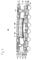
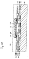
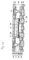
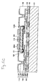
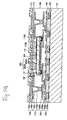
- Fig. 1 is a sectional view schematically showing a wiring board 100 according to a first embodiment of the present invention.
- the wiring board according to the present invention has an insulating layer 106 having a semiconductor chip 110 embedded and made of what is called a build-up resin material such as an epoxy.
- Reinforcing layers 103 and 114 for reinforcing the insulating layer 106 are respectively formed so as to come into contact with both the surfaces of the insulating layer 106.
- the semiconductor chip 110 is connected to a wiring section (described below) and connected through the wiring section to an electrode 102 formed in the side of the reinforcing layer 103 (a lower side in the drawing, hereinafter) or an electrode 118 formed in the side of the reinforcing layer 114 (an upper side in the drawing, hereinafter).
- the electrode 102 or the electrode 118 is connected to a mother board or other devices, or connecting devices.
- stud bumps 111 made of, for instance, Au are formed.
- the stud bump 111 is connected to a wiring section 108 embedded in the insulating layer 106 through, for instance, a solder connecting section 109. Further, in the lower side of the semiconductor chip 110, an under-fill layer 110A may be formed.
- a wiring section 105, a wiring section 113 and a wiring section 116 are formed with, for instance, Cu so as to be laminated in addition to the wiring section 108.
- the wiring section 105 includes a via-plug 105a and a pattern wiring 105b.
- the via-plug 105a is formed in an opening portion formed in the reinforcing layer 103.
- the pattern wiring 105b connected to the via-plug 105a is formed.
- the wiring section 108 connected to the wiring section 105 is formed and embedded in the insulating layer 106.
- the wiring section 108 includes a via-plug 108a formed on the pattern wiring 105b and a pattern wiring 108b connected to the via-plug 108a. To the pattern wiring 108b, the semiconductor chip 110 is connected through the solder connecting section 109 and the stud bump 111 as described above.
- the wiring section 113 includes a via-plug 113a formed on the pattern wiring 108b and a pattern wiring 113b connected to the via-plug 113a.
- the wiring section 116 includes a via-plug 116a formed on the pattern wiring 113b and a pattern wiring 116b connected to the via plug 116a.
- the via-plug 116a is formed in an opening portion formed from the insulating layer 106 side to the reinforcing layer 114 and the pattern wiring 116b is formed on the reinforcing layer 114.
- the electrode 102 connected to the via-plug 105a is formed in an opening portion of the reinforcing layer 103.
- the electrode 118 is formed respectively.
- solder resist layers 119 and 117 are respectively formed so as to cover the reinforcing layer 103 and the reinforcing layer 114 therewith. On the solder resist layers, opening portions for exposing the electrodes are formed.
- solder ball 120 is formed in the electrode 102 as required.
- a solder ball may be formed in the electrode 118.
- the insulating layer 106 in which the semiconductor chip or the wiring sections are embedded is formed so as to be sandwiched in between the reinforcing layer 103 and the reinforcing layer 114. Therefore, the wiring board can be formed in which the warpage of the wiring board having the semiconductor chip incorporated is reduced and that is high in its flatness and can meet a finely formed wiring.
- the reinforcing layers 103 and 114 are preferably formed by using a prepreg material.
- the prepreg material is referred to as an organic core material, or sometimes simply referred to as a core material, and may be used as a material of a core board when a multi-layer wiring board (a build-up board) is formed.
- the prepreg material has a structure that an epoxy type resin material is impregnated with glass fibers and solidified, and shows a feature that rigidity is higher than that of an ordinary build-up resin material.
- amodulusof elasticity (Young's modulus) of the build-up resin material is about 5 GPa to 8 GPa.
- the modulus of elasticity of the prepreg material is 20 GPa or more and the prepreg material has high rigidity. Consequently, the warpage of the wiring board is be reduced.
- the material with which the reinforcing layers 103 and 114 are formed is not limited to the prepreg material, and, for instance, a mold resin having high rigidity may be employed. Further, as a material forming the reinforcing layers 103 and 114, a material such as metal may be used. When an electric conductive material such as metal is used, a structure for insulating the wiring section from the reinforcing layer is preferably added.
- the wiring board according to this embodiment can be formed in accordance with the usual build-up method, and the thickness of the wiring board can be reduced.
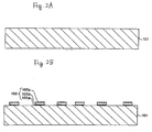
- a supporting board 101 is prepared that is made of an electric conductive material, for instance, Cu and has the thickness of 200 ⁇ m.
- a resist pattern (not shown in the drawing) is formed on the supporting board 101 by a photolithography method and the electrode 102 is formed having a structure that for instance, an Au layer 102a, an Ni layer 102b and a Cu layer 102c are laminated by an electrolytic plating with the resist pattern used as a mask.
- the supporting board 101 since the supporting board 101 serves as a path through which an electric current is supplied, the supporting board 101 is preferably made of the electric conductive material, and more preferably made of a material having a low resistance, such as Cu.
- the reinforcing layer 103 made of the prepreg material is formed on the supporting board 101 so as to cover the electrode 102 therewith.
- a via-hole 103A is formed by, for instance, a laser so as to expose the electrode 102.
- a desmear process is carried out as required to remove residue materials of the via-hole and perform a surface treatment of the reinforcing layer 103, and then, a seed layer 104 of Cu is formed on the surface of the reinforcing layer 103 and the surface of the electrode 102 by an electroless plating process.
- a resist pattern (not shown in the drawing) is formed by the photolithography method.
- the via-plug 105a is formed in the via-hole 103A and the pattern wiring 105b connected to the via-plug 105a is formed on the reinforcing layer 103 by the electrolytic plating of Cu using the resist pattern as a mask to form the wiring section 105.
- the resist pattern is separated to remove an exposed surplus seed layer by etching.
- the insulating layer 106 (a build-up layer) made of, for instance, a thermosetting epoxy resin is formed on the reinforcing layer 103 so as to cover the wiring section 105 therewith. Further, in the insulating layer, a via-hole 106A is formed by a laser so that a part of the pattern wiring 105b is exposed.
- a desmear process is carried out as required in the same manner as that of the process shown in Fig. 2D to remove residue materials of the via-hole and perform a surface treatment of the insulating layer 106, and then, a seed layer 107 of Cu is formed on the surface of the insulating layer 106 and the exposed surface of the pattern wiring 105b by the electroless plating process.
- a resist pattern (not shown in the drawing) is formed by the photolithography method in the same manner as that of the process shown in Fig. 2E.
- the via-plug 108a is formed in the via-hole 106A and the pattern wiring 108b connected to the via-plug 108a is formed on the insulating layer 106 by the electrolytic plating of Cu using the resist pattern as a mask to form the wiring section 108.
- the resist pattern is peeled from the seed layer to remove an exposed surplus seed layer by etching.
- an insulating layer (a build-up layer) 106a made of, for instance, a thermosetting epoxy resin is formed on the insulating layer 106 so as to cover the wiring section 108 therewith. Since the insulating layer 106a is substantially entirely formed integrally with the insulating layer 106, the insulating layer 106 is referred to as a layer including the insulating layer 106a after Fig. 2I.
- an opening portion 106B is formed on the insulating layer 106 by, for instance, a laser so as to expose a part of the pattern wiring 108b.
- a desmear process is carried out as required to remove the residue materials of the opening portion and perform the surface treatment of the insulating layer 106, and then, the solder connecting section 109 is formed in the opening portion 106B by, for instance, the electrolytic plating process.
- the semiconductor chip 110 having the stud bump 111 made of, for instance, Au is mounted on the wiring section 108 so that the stud bump 111 corresponds to the solder connecting section 109.
- a re-flow process of the solder connecting section 109 is preferably carried out if necessary to satisfactorily achieve the electric connection of the solder connecting section 109 to the stud bump 111.
- the under-fill layer 110A is preferably formed between the semiconductor chip 110 and the insulating layer 106 as required.
- an insulating layer (a build-up layer) 106b made of, for instance, a thermosetting epoxy resin is formed on the insulating layer 106 so as to cover the semiconductor chip 110 therewith. Since the insulating layer 106b is substantially entirely formed integrally with the insulating layer 106, the insulating layer 106 is referred to as a layer including the insulating layer 106b after Fig. 2M.
- a via-hole 106C is formed on the insulating layer 106 by, for instance, a laser so as to expose a part of the pattern wiring 108b.
- a desmear process is carried out as required to remove the residue materials of the via-hole and perform the surface treatment of the insulating layer 106, and then, a seed layer 112 of Cu is formed on the surface of the insulating layer 106 and the surface of the pattern wiring 108b by the electroless plating process.
- a resist pattern (not shown in the drawing) is formed by the photolithography method in the same manner as that of the process shown in Fig. 2H. Then, the via-plug 113a is formed in the via-hole 106C and the pattern wiring 113b connected to the via-plug 113a is formed on the insulating layer 106 by the electrolytic plating of Cu using the resist pattern as a mask to form the wiring section 113.
- the resist pattern is peeled from the seed layer to remove an exposed surplus seed layer by etching.
- an insulating layer (a build-up layer) 106c made of, for instance, a thermosetting epoxy resin is formed on the insulating layer 106 so as to cover the wiring section 113 therewith. Since the insulating layer 106c is substantially entirely formed integrally with the insulating layer 106, the insulating layer 106 is referred to as a layer including the insulating layer 106c after Fig. 2P.
- the reinforcing layer 114 made of, for instance, the prepreg material is formed on the insulating layer 106c. After the reinforcing layer 114 is formed, via-holes 114A are formed in the reinforcing layer 114 and the insulating layer 106 by, for instance, a laser so as to expose the pattern wiring 113b.
- a desmear process is carried out as required to remove the residue materials of the via-holes and perform the surface treatments of the insulating layer 106 and the reinforcing layer 114, and then, a seed layer 115 of Cu is formed on the inner wall surfaces of the via-holes, the surface of the reinforcing layer 114, and the surface of the pattern wiring 113b by the electroless plating process.
- a resist pattern (not shown in the drawing) is formed by the photolithography method in the same manner as that of the process shown in Fig. 20.
- the via-plug 116a is formed in the via-hole 114A and the pattern wiring 116b connected to the via-plug 116a is formed on the reinforcing layer 114 by the electrolytic plating of Cu using the resist pattern as a mask to form the wiring section 116.
- the resist pattern is peeled from the seed layer to remove an exposed surplus seed layer by etching.
- solder resist layer 117 having an opening portion 117A from which a part of the pattern wiring 116b is exposed is formed so as to cover the reinforcing layer 114 therewith.
- the electrode 118 made of, for instance, Ni/Au is formed on the pattern wiring 116b exposed from the opening portion 117A.
- the supporting board 101 is removed by, for instance, a wet etching process.
- the solder resist layer 119 having an opening portion 119A from which the electrode 102 is exposed is formed so as to cover the reinforcing layer 103 therewith.
- solder ball 120 is formed in the electrode 102, so that the wiring board 100 shown in Fig. 1 can be formed.
- the thin, compact and light wiring board can be realized, and the warpage can be reduced by the reinforcing layers 103 and 114. Accordingly, the wiring board having the finely formed wiring sections and the small thickness can be formed.
- the reinforcing layer 103 is preferably formed so as to be thicker than the reinforcing layer 114, because in the processes of manufacturing the wiring board, the number of times of having heat stress is increased more toward the lower layer.
- the insulating layer 106 is formed by laminating the thermosetting resin materials.
- a thermosetting process is preferably provided. Therefore, since the number of times of having the heat stress is increased in the lower (a lower layer side) reinforcing layer of the wiring board, the lower reinforcing layer is preferably formed to be thicker than the upper (an upper layer side) reinforcing layer to reduce the warpage.
- the thickness of the wiring board 100 for instance, when the thickness of the reinforcing layer 103 is set to 80 ⁇ m and the thickness of the reinforcing layer 114 is 40 ⁇ m, the wiring board having the entire thickness of 440 ⁇ m can be formed.
- the supporting board 101 made of, for example, Cu is removed by etching.
- the supporting board 101 may be provided with a release layer on a side to be in contact with the reinforcing layer 103, by preparing the supporting board 101 onto which an adhesive release tape is applied, for example.
- adhesive strength of the release layer lowers by being heated.
- the reinforcing layer 103 is peeled off from the release layer by heating the entire wiring board with, for instance, an oven.
- the wiring board described in the first embodiment can be formed in a structure in which the warpage is more reduced as described below.
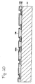
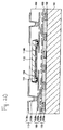
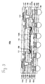
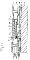
- Fig. 3 is a sectional view schematically showing a wiring board 100A according to a second embodiment.
- the previously described parts are designated by the same reference numerals and an explanation thereof is omitted.
- a reinforcing layer 121 that reinforces an insulating layer 106 is embedded in the insulating layer 106 and formed between a reinforcing layer 103 and a reinforcing layer 114.
- the reinforcing layer 121 an opening portion 121A through which a via-plug 113a passes is formed.
- the reinforcing layer is further added to the insulating layer 106 in addition to the structure shown in the first embodiment, so that the rigidity of the wiring board is more improved and an effect for suppressing the warpage of the wiring board is more increased.
- the wiring board 100A according to this embodiment is produced, in the manufacturing method described in the first embodiment, a process for forming the reinforcing layer 121 may be added after the process shown in Fig. 2L. Subsequent processes are the same as those of the first embodiment. Thus, the wiring board 100A can be produced.
- the reinforcing layer 121 is made of, for instance, a prepreg material like the reinforcing layers 103 and 114, however, may be formed by using a mold resin or a metal material.
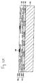
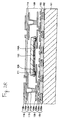
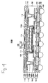
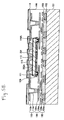
- Fig. 4 is a sectional view schematically showing a wiring board 100B according to a third embodiment of the present invention.
- the previously described parts are designated by the same reference numerals and an explanation thereof is omitted.
- a heat radiating section 200 is formed for radiating the heat (cooling) of a semiconductor chip 110.
- the heat radiating section 200 includes a metal layer 201 formed on the semiconductor chip 110, a heat radiating via-plug 202 connected to the metal layer 201 and formed so as to stand on the metal layer 201 and an electrode 203 formed on the heat radiating via-plug 202 and made of, for instance, Ni/Au.
- the metal layer has a structure of Cr/Cu or Ti/Cu and is formed on the back side of a device surface of the semiconductor chip 110.
- the heat radiating via-plug 202 is made of, for instance, Cu, connected to the metal layer 201 and formed so as to stand on the metal layer 201 and allow its side surfaces to come into contact with an insulating layer 106, a reinforcing layer 114 and a solder resist layer 117.
- the metal layer 201 and the heat radiating via-plug 202 are formed, the heat generated in the semiconductor chip 110 can be efficiently radiated. Accordingly, the breakage of the semiconductor chip or an imperfect operation or the warpage of the wiring board due to the heat can be effectively suppressed.
- the electrode 203 is formed on the heat radiating via-plug 202 exposed from an opening portion formed in the solder resist layer 117. For instance, on the electrode 203, a solder ball is formed as required.
- the electrode can be connected to an object to be connected to the wiring board such as a mother board. For instance, when the heat radiating via-plug 202 is connected to the object to be connected through the electrode 203, the heat is more efficiently radiated to efficiently expel the heat generated in the semiconductor chip to the object to be connected.
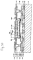
- a process shown in Fig. 5A corresponds to the process shown in Fig. 2M of the manufacturing method described in the first embodiment. That is, the processes shown in Figs. 2A to 2M of the first embodiment are carried out to obtain a state shown in Fig. 5A.
- the metal layer 201 having the structure made of, for instance, Cr/Cu or Ti/Cu is formed on the back side of the device forming surface of the semiconductor chip 110 by a sputtering method.
- a via-hole 106C is formed on the insulating layer 106 and a via-hole 106D reaching the metal layer 201 is formed by, for instance, a laser.
- the metal layer functions as the stopper layer of the laser to prevent the device formed on the semiconductor chip from being damaged by the laser. That is, the metal layer 201 contributes to the heat radiation and serves as a protecting layer of the device of the semiconductor chip in the processes for manufacturing the wiring board. Further, the metal layer effectively improves the adhesive force between a heat radiating via-plug formed in the via-hole in a subsequent process and the semiconductor chip.
- a desmear process is carried out as required to remove the residue materials of the via-holes and perform a surface treatment of the insulating layer 106.
- a seed layer 112 of Cu is formed on the surface of the insulating layer 106 including the inner wall surfaces of the via-holes, the surface of a pattern wiring 108b, and the surface of the metal layer 201 by an electroless plating process.
- a wiring section 113 is formed and a heat-radiating via plug 202A is formed in the via-hole 106D.
- an insulating layer 106c is formed in the same manner as that of the first embodiment to form the reinforcing layer 114 made of, for instance, prepreg material on the insulating layer 106c. Further, a via-hole 114A is formed and a via-hole 114B is formed on the prepreg material 114 by, for instance, a laser.
- a desmear process is carried out if necessary to remove the residue materials of the via-holes and perform the surface treatments of the insulating layer 106 and the reinforcing layer 114.
- a seed layer 115 of Cu is formed on the inner wall surfaces of the via-holes 114A and 114B, the surface of the reinforcing layer 114, the surface of a pattern wiring 113b and the surface of the heat radiating via-plug 202A.
- a wiring section 116 is formed by an electrolytic plating process of Cu and a heat radiating via-plug 202B is formed so as to be laminated on the heat-radiating via-plug 202A.
- the heat radiating via-plug 202 including the heat radiating via-plugs 202A and 202B is formed.
- a resist pattern is peeled to remove the exposed surplus seed layer by an etching process.
- the wiring board can be formed in the same manner as that of the first embodiment except that in a process shown in Fig. 5G, an opening portion 117B is formed from which the heat radiating via-plug 202 is exposed is formed on the solder resist layer 117, and in a process shown in Fig.5H, when an electrode 118 is formed, the electrode 203 is formed on the heat radiating via plug 202.
- the heat radiating section of the semiconductor chip can be formed without increasing the number of processes as compared with the manufacturing method of the first embodiment.
- the structure of the heat radiating section is not limited to this embodiment, and, for instance, materials thereof (kinds of metal materials) or structures thereof (the number of heat radiating via-plugs, positions thereof, etc.) may be variously modified and changed.
- the small thickness of a wiring board in which a semiconductor chip is incorporated can be realized and the warpage of the wiring board can be suppressed.
Landscapes
- Engineering & Computer Science (AREA)
- Manufacturing & Machinery (AREA)
- Microelectronics & Electronic Packaging (AREA)
- Production Of Multi-Layered Print Wiring Board (AREA)
- Structure Of Printed Boards (AREA)
Applications Claiming Priority (1)
| Application Number | Priority Date | Filing Date | Title |
|---|---|---|---|
| JP2005162547A JP4016039B2 (ja) | 2005-06-02 | 2005-06-02 | 配線基板および配線基板の製造方法 |
Publications (3)
| Publication Number | Publication Date |
|---|---|
| EP1740025A2 true EP1740025A2 (de) | 2007-01-03 |
| EP1740025A3 EP1740025A3 (de) | 2009-04-08 |
| EP1740025B1 EP1740025B1 (de) | 2018-08-29 |
Family
ID=37434054
Family Applications (1)
| Application Number | Title | Priority Date | Filing Date |
|---|---|---|---|
| EP06011507.8A Ceased EP1740025B1 (de) | 2005-06-02 | 2006-06-02 | Leiterplatte und Verfahren zu deren Herstellung |
Country Status (6)
| Country | Link |
|---|---|
| US (1) | US7732712B2 (de) |
| EP (1) | EP1740025B1 (de) |
| JP (1) | JP4016039B2 (de) |
| KR (1) | KR101160528B1 (de) |
| CN (1) | CN1882224B (de) |
| TW (1) | TWI408780B (de) |
Cited By (2)
| Publication number | Priority date | Publication date | Assignee | Title |
|---|---|---|---|---|
| EP2448380A1 (de) * | 2010-10-26 | 2012-05-02 | ATOTECH Deutschland GmbH | Verbundtoffbaumaterial zum Einbetten eines Schaltkreises |
| EP2448378A1 (de) * | 2010-10-26 | 2012-05-02 | ATOTECH Deutschland GmbH | Verbundtoffbaumaterialien zum Einbetten aktiver Komponenten |
Families Citing this family (35)
| Publication number | Priority date | Publication date | Assignee | Title |
|---|---|---|---|---|
| US20080122061A1 (en) * | 2006-11-29 | 2008-05-29 | Texas Instruments Incorporated | Semiconductor chip embedded in an insulator and having two-way heat extraction |
| JP5326269B2 (ja) * | 2006-12-18 | 2013-10-30 | 大日本印刷株式会社 | 電子部品内蔵配線板、及び電子部品内蔵配線板の放熱方法 |
| US20100103634A1 (en) * | 2007-03-30 | 2010-04-29 | Takuo Funaya | Functional-device-embedded circuit board, method for manufacturing the same, and electronic equipment |
| JP5289880B2 (ja) * | 2007-10-12 | 2013-09-11 | 新光電気工業株式会社 | 配線基板 |
| US10074553B2 (en) | 2007-12-03 | 2018-09-11 | STATS ChipPAC Pte. Ltd. | Wafer level package integration and method |
| US9460951B2 (en) * | 2007-12-03 | 2016-10-04 | STATS ChipPAC Pte. Ltd. | Semiconductor device and method of wafer level package integration |
| CN101452935B (zh) * | 2007-12-05 | 2011-12-21 | 群康科技(深圳)有限公司 | 芯片与晶圆 |
| TWI356479B (en) * | 2008-03-04 | 2012-01-11 | Advanced Semiconductor Eng | Package structure with embedded die and method of |
| JP5295596B2 (ja) * | 2008-03-19 | 2013-09-18 | 新光電気工業株式会社 | 多層配線基板およびその製造方法 |
| CN102047403A (zh) * | 2008-06-02 | 2011-05-04 | Nxp股份有限公司 | 电子器件及电子器件的制造方法 |
| KR101003585B1 (ko) * | 2008-06-25 | 2010-12-22 | 삼성전기주식회사 | 전자부품 내장형 인쇄회로기판 및 그 제조방법 |
| TWI401000B (zh) * | 2008-07-23 | 2013-07-01 | 日本電氣股份有限公司 | 無核心層配線基板、半導體裝置及其製造方法 |
| WO2010024233A1 (ja) | 2008-08-27 | 2010-03-04 | 日本電気株式会社 | 機能素子を内蔵可能な配線基板及びその製造方法 |
| JP5012779B2 (ja) * | 2008-12-08 | 2012-08-29 | 日本電気株式会社 | 半導体装置 |
| JP2010205851A (ja) * | 2009-03-02 | 2010-09-16 | Shinko Electric Ind Co Ltd | 半導体装置及びその製造方法、並びに電子装置 |
| JPWO2010101167A1 (ja) * | 2009-03-05 | 2012-09-10 | 日本電気株式会社 | 半導体装置及びその製造方法 |
| KR101056156B1 (ko) * | 2009-11-24 | 2011-08-11 | 삼성전기주식회사 | 인쇄회로기판 제조용 절연체 및 이를 이용한 전자소자 내장형 인쇄회로기판 제조방법 |
| WO2011089936A1 (ja) * | 2010-01-22 | 2011-07-28 | 日本電気株式会社 | 機能素子内蔵基板及び配線基板 |
| FR2964790A1 (fr) * | 2010-09-13 | 2012-03-16 | St Microelectronics Grenoble 2 | Composant et dispositif semi-conducteur munis de moyens de dissipation de chaleur |
| JP5879030B2 (ja) * | 2010-11-16 | 2016-03-08 | 新光電気工業株式会社 | 電子部品パッケージ及びその製造方法 |
| JP2013211519A (ja) | 2012-02-29 | 2013-10-10 | Ngk Spark Plug Co Ltd | 多層配線基板の製造方法 |
| CN103906372B (zh) * | 2012-12-27 | 2017-03-01 | 碁鼎科技秦皇岛有限公司 | 具有内埋元件的电路板及其制作方法 |
| KR102250997B1 (ko) | 2014-05-02 | 2021-05-12 | 삼성전자주식회사 | 반도체 패키지 |
| JP6358431B2 (ja) * | 2014-08-25 | 2018-07-18 | 新光電気工業株式会社 | 電子部品装置及びその製造方法 |
| US10079156B2 (en) | 2014-11-07 | 2018-09-18 | Advanced Semiconductor Engineering, Inc. | Semiconductor package including dielectric layers defining via holes extending to component pads |
| US9721799B2 (en) | 2014-11-07 | 2017-08-01 | Advanced Semiconductor Engineering, Inc. | Semiconductor package with reduced via hole width and reduced pad patch and manufacturing method thereof |
| US9420695B2 (en) | 2014-11-19 | 2016-08-16 | Advanced Semiconductor Engineering, Inc. | Semiconductor package structure and semiconductor process |
| US9426891B2 (en) | 2014-11-21 | 2016-08-23 | Advanced Semiconductor Engineering, Inc. | Circuit board with embedded passive component and manufacturing method thereof |
| US10325853B2 (en) | 2014-12-03 | 2019-06-18 | Taiwan Semiconductor Manufacturing Company, Ltd. | Method of forming semiconductor packages having through package vias |
| TWI654723B (zh) * | 2015-02-06 | 2019-03-21 | 矽品精密工業股份有限公司 | 封裝結構之製法 |
| DE102016119825A1 (de) * | 2016-10-18 | 2018-04-19 | HELLA GmbH & Co. KGaA | Leiterplatte |
| KR102019355B1 (ko) | 2017-11-01 | 2019-09-09 | 삼성전자주식회사 | 반도체 패키지 |
| KR102029101B1 (ko) * | 2017-12-28 | 2019-10-07 | 삼성전자주식회사 | 반도체 패키지 |
| US11432402B2 (en) * | 2018-10-11 | 2022-08-30 | Microchip Technology Caldicot Limited | Flipped-conductor-patch lamination for ultra fine-line substrate creation |
| US11848280B2 (en) * | 2020-11-25 | 2023-12-19 | ADVANCED SEMlCONDUCTOR ENGINEERING, INC. | Method for manufacturing assembly structure by using frame structure on substrate |
Citations (3)
| Publication number | Priority date | Publication date | Assignee | Title |
|---|---|---|---|---|
| US20040160752A1 (en) | 2003-02-18 | 2004-08-19 | Matsushita Electric Industrial Co. | Electronic component built-in module and method of manufacturing the same |
| US20050006142A1 (en) | 2003-07-09 | 2005-01-13 | Matsushita Electric Industrial Co., Ltd. | Circuit board with in-built electronic component and method for manufacturing the same |
| WO2005004567A1 (ja) | 2003-07-04 | 2005-01-13 | Murata Manufacturing Co., Ltd. | 部品内蔵基板の製造方法 |
Family Cites Families (22)
| Publication number | Priority date | Publication date | Assignee | Title |
|---|---|---|---|---|
| US4979076A (en) * | 1989-06-30 | 1990-12-18 | Dibugnara Raymond | Hybrid integrated circuit apparatus |
| US6239976B1 (en) * | 1998-11-24 | 2001-05-29 | Comsense Technologies, Ltd. | Reinforced micromodule |
| US6320135B1 (en) * | 1999-02-03 | 2001-11-20 | Casio Computer Co., Ltd. | Flexible wiring substrate and its manufacturing method |
| JP2001085804A (ja) * | 1999-09-17 | 2001-03-30 | Sony Corp | プリント配線板およびその製造方法 |
| JP3540976B2 (ja) * | 2000-02-29 | 2004-07-07 | 京セラ株式会社 | 電気素子内蔵配線基板 |
| JP2001313468A (ja) * | 2000-04-28 | 2001-11-09 | Kyocera Corp | 配線基板 |
| JP2001352007A (ja) | 2000-06-08 | 2001-12-21 | Sumitomo Metal Ind Ltd | 多層配線基板とその製造方法及びそれを用いた接続構造 |
| JP2002076637A (ja) | 2000-08-29 | 2002-03-15 | Matsushita Electric Ind Co Ltd | チップ部品内蔵基板及びその製造方法 |
| JP2002093957A (ja) * | 2000-09-11 | 2002-03-29 | Sony Corp | 電子回路装置およびその製造方法 |
| JP4040389B2 (ja) * | 2001-09-27 | 2008-01-30 | 大日本印刷株式会社 | 半導体装置の製造方法 |
| JP2003115664A (ja) * | 2001-10-05 | 2003-04-18 | Matsushita Electric Ind Co Ltd | 電圧変換モジュール |
| JP2003142628A (ja) | 2001-11-08 | 2003-05-16 | Ngk Spark Plug Co Ltd | 配線基板 |
| JP3492348B2 (ja) * | 2001-12-26 | 2004-02-03 | 新光電気工業株式会社 | 半導体装置用パッケージの製造方法 |
| JP3591524B2 (ja) * | 2002-05-27 | 2004-11-24 | 日本電気株式会社 | 半導体装置搭載基板とその製造方法およびその基板検査法、並びに半導体パッケージ |
| JP4378511B2 (ja) * | 2002-07-25 | 2009-12-09 | 大日本印刷株式会社 | 電子部品内蔵配線基板 |
| JP4119205B2 (ja) * | 2002-08-27 | 2008-07-16 | 富士通株式会社 | 多層配線基板 |
| JP4103549B2 (ja) * | 2002-10-31 | 2008-06-18 | 株式会社デンソー | 多層配線基板の製造方法及び多層配線基板 |
| JP2004343021A (ja) * | 2003-03-17 | 2004-12-02 | Matsushita Electric Ind Co Ltd | 部品内蔵モジュールの製造方法及び製造装置 |
| JP2004327624A (ja) | 2003-04-23 | 2004-11-18 | Shinko Electric Ind Co Ltd | 部品内蔵多層回路基板 |
| JP2004356447A (ja) * | 2003-05-29 | 2004-12-16 | Toshiba Corp | プリント配線基板及びその製造方法 |
| JP2005072061A (ja) * | 2003-08-27 | 2005-03-17 | Ngk Spark Plug Co Ltd | 配線基板およびその製造方法 |
| JP4575071B2 (ja) * | 2004-08-02 | 2010-11-04 | 新光電気工業株式会社 | 電子部品内蔵基板の製造方法 |
-
2005
- 2005-06-02 JP JP2005162547A patent/JP4016039B2/ja not_active Expired - Fee Related
-
2006
- 2006-05-19 KR KR1020060045339A patent/KR101160528B1/ko not_active Expired - Fee Related
- 2006-06-01 US US11/421,607 patent/US7732712B2/en not_active Expired - Fee Related
- 2006-06-01 TW TW095119359A patent/TWI408780B/zh not_active IP Right Cessation
- 2006-06-02 CN CN2006100833472A patent/CN1882224B/zh not_active Expired - Fee Related
- 2006-06-02 EP EP06011507.8A patent/EP1740025B1/de not_active Ceased
Patent Citations (3)
| Publication number | Priority date | Publication date | Assignee | Title |
|---|---|---|---|---|
| US20040160752A1 (en) | 2003-02-18 | 2004-08-19 | Matsushita Electric Industrial Co. | Electronic component built-in module and method of manufacturing the same |
| WO2005004567A1 (ja) | 2003-07-04 | 2005-01-13 | Murata Manufacturing Co., Ltd. | 部品内蔵基板の製造方法 |
| US20050006142A1 (en) | 2003-07-09 | 2005-01-13 | Matsushita Electric Industrial Co., Ltd. | Circuit board with in-built electronic component and method for manufacturing the same |
Cited By (6)
| Publication number | Priority date | Publication date | Assignee | Title |
|---|---|---|---|---|
| EP2448380A1 (de) * | 2010-10-26 | 2012-05-02 | ATOTECH Deutschland GmbH | Verbundtoffbaumaterial zum Einbetten eines Schaltkreises |
| EP2448378A1 (de) * | 2010-10-26 | 2012-05-02 | ATOTECH Deutschland GmbH | Verbundtoffbaumaterialien zum Einbetten aktiver Komponenten |
| WO2012055785A1 (en) * | 2010-10-26 | 2012-05-03 | Atotech Deutschland Gmbh | Composite build-up materials for embedding of active components |
| WO2012055789A1 (en) * | 2010-10-26 | 2012-05-03 | Atotech Deutschland Gmbh | Composite build-up material for embedding of circuitry |
| US20130199832A1 (en) * | 2010-10-26 | 2013-08-08 | Atotech Deutschland Gmbh | Composite build-up materials for embedding of active components |
| JP2013545297A (ja) * | 2010-10-26 | 2013-12-19 | アトテツク・ドイチユラント・ゲゼルシヤフト・ミツト・ベシユレンクテル・ハフツング | 回路素子を埋め込むための複合ビルドアップ材料 |
Also Published As
| Publication number | Publication date |
|---|---|
| US7732712B2 (en) | 2010-06-08 |
| EP1740025A3 (de) | 2009-04-08 |
| KR20060125472A (ko) | 2006-12-06 |
| JP4016039B2 (ja) | 2007-12-05 |
| EP1740025B1 (de) | 2018-08-29 |
| US20060272854A1 (en) | 2006-12-07 |
| TWI408780B (zh) | 2013-09-11 |
| TW200703591A (en) | 2007-01-16 |
| CN1882224A (zh) | 2006-12-20 |
| CN1882224B (zh) | 2010-12-29 |
| KR101160528B1 (ko) | 2012-06-28 |
| JP2006339421A (ja) | 2006-12-14 |
Similar Documents
| Publication | Publication Date | Title |
|---|---|---|
| EP1740025B1 (de) | Leiterplatte und Verfahren zu deren Herstellung | |
| US7937828B2 (en) | Method of manufacturing wiring board | |
| JP3988998B2 (ja) | メッキ引込線なしにメッキされるパッケージ基板の製造方法 | |
| US7884484B2 (en) | Wiring board and method of manufacturing the same | |
| KR101344800B1 (ko) | 배선 기판 및 반도체 장치 | |
| US7842541B1 (en) | Ultra thin package and fabrication method | |
| JP2010135721A (ja) | 金属バンプを持つプリント基板及びその製造方法 | |
| US9334576B2 (en) | Wiring substrate and method of manufacturing wiring substrate | |
| JP2006049424A (ja) | 電子部品内蔵基板およびその製造方法 | |
| JP2010287742A (ja) | 配線基板の製造方法 | |
| JP2004193549A (ja) | メッキ引込線なしにメッキされたパッケージ基板およびその製造方法 | |
| JP2011228737A (ja) | 配線基板、及び半導体装置 | |
| US7772109B2 (en) | Manufacturing method of multilayer wiring substrate | |
| KR20140143567A (ko) | 반도체 패키지 기판 및 반도체 패키지 기판 제조 방법 | |
| JP4170266B2 (ja) | 配線基板の製造方法 | |
| JP5479638B2 (ja) | 配線基板 | |
| KR101489798B1 (ko) | 배선 기판 | |
| JP2013058775A (ja) | 半導体パッケージ基板の製造方法 | |
| KR20120039163A (ko) | 인쇄회로기판 및 그 제조방법 | |
| CN113380720B (zh) | 线路载板结构及其制作方法 | |
| JP5574132B2 (ja) | 配線基板および半導体パッケージ | |
| JP2006049822A (ja) | 半導体ic内蔵モジュール | |
| JP2017118084A (ja) | プリント回路基板 | |
| JP4549691B2 (ja) | 配線基板の製造方法 | |
| KR101109216B1 (ko) | 인쇄회로기판의 제조방법 |
Legal Events
| Date | Code | Title | Description |
|---|---|---|---|
| PUAI | Public reference made under article 153(3) epc to a published international application that has entered the european phase |
Free format text: ORIGINAL CODE: 0009012 |
|
| AK | Designated contracting states |
Kind code of ref document: A2 Designated state(s): AT BE BG CH CY CZ DE DK EE ES FI FR GB GR HU IE IS IT LI LT LU LV MC NL PL PT RO SE SI SK TR |
|
| AX | Request for extension of the european patent |
Extension state: AL BA HR MK YU |
|
| PUAL | Search report despatched |
Free format text: ORIGINAL CODE: 0009013 |
|
| AK | Designated contracting states |
Kind code of ref document: A3 Designated state(s): AT BE BG CH CY CZ DE DK EE ES FI FR GB GR HU IE IS IT LI LT LU LV MC NL PL PT RO SE SI SK TR |
|
| AX | Request for extension of the european patent |
Extension state: AL BA HR MK YU |
|
| 17P | Request for examination filed |
Effective date: 20090811 |
|
| AKX | Designation fees paid |
Designated state(s): DE |
|
| 17Q | First examination report despatched |
Effective date: 20130524 |
|
| GRAP | Despatch of communication of intention to grant a patent |
Free format text: ORIGINAL CODE: EPIDOSNIGR1 |
|
| INTG | Intention to grant announced |
Effective date: 20171025 |
|
| GRAJ | Information related to disapproval of communication of intention to grant by the applicant or resumption of examination proceedings by the epo deleted |
Free format text: ORIGINAL CODE: EPIDOSDIGR1 |
|
| INTC | Intention to grant announced (deleted) | ||
| GRAS | Grant fee paid |
Free format text: ORIGINAL CODE: EPIDOSNIGR3 |
|
| GRAP | Despatch of communication of intention to grant a patent |
Free format text: ORIGINAL CODE: EPIDOSNIGR1 |
|
| INTG | Intention to grant announced |
Effective date: 20180530 |
|
| GRAA | (expected) grant |
Free format text: ORIGINAL CODE: 0009210 |
|
| AK | Designated contracting states |
Kind code of ref document: B1 Designated state(s): DE |
|
| REG | Reference to a national code |
Ref country code: DE Ref legal event code: R096 Ref document number: 602006056188 Country of ref document: DE |
|
| REG | Reference to a national code |
Ref country code: DE Ref legal event code: R097 Ref document number: 602006056188 Country of ref document: DE |
|
| PLBE | No opposition filed within time limit |
Free format text: ORIGINAL CODE: 0009261 |
|
| STAA | Information on the status of an ep patent application or granted ep patent |
Free format text: STATUS: NO OPPOSITION FILED WITHIN TIME LIMIT |
|
| 26N | No opposition filed |
Effective date: 20190531 |
|
| PGFP | Annual fee paid to national office [announced via postgrant information from national office to epo] |
Ref country code: DE Payment date: 20200519 Year of fee payment: 15 |
|
| REG | Reference to a national code |
Ref country code: DE Ref legal event code: R119 Ref document number: 602006056188 Country of ref document: DE |
|
| PG25 | Lapsed in a contracting state [announced via postgrant information from national office to epo] |
Ref country code: DE Free format text: LAPSE BECAUSE OF NON-PAYMENT OF DUE FEES Effective date: 20220101 |