EP1740904B1 - Mesure de l'epaisseur d'une couche mince au moyen d'un capteur infrarouge multicanaux - Google Patents
Mesure de l'epaisseur d'une couche mince au moyen d'un capteur infrarouge multicanaux Download PDFInfo
- Publication number
- EP1740904B1 EP1740904B1 EP05740132A EP05740132A EP1740904B1 EP 1740904 B1 EP1740904 B1 EP 1740904B1 EP 05740132 A EP05740132 A EP 05740132A EP 05740132 A EP05740132 A EP 05740132A EP 1740904 B1 EP1740904 B1 EP 1740904B1
- Authority
- EP
- European Patent Office
- Prior art keywords
- film
- filters
- transmitted
- energy
- measured
- Prior art date
- Legal status (The legal status is an assumption and is not a legal conclusion. Google has not performed a legal analysis and makes no representation as to the accuracy of the status listed.)
- Expired - Lifetime
Links
- 238000005259 measurement Methods 0.000 title description 17
- 239000010409 thin film Substances 0.000 title description 14
- 238000000034 method Methods 0.000 claims description 29
- 230000003595 spectral effect Effects 0.000 claims description 24
- 239000000523 sample Substances 0.000 claims description 21
- 238000004422 calculation algorithm Methods 0.000 claims description 10
- 230000005855 radiation Effects 0.000 claims description 9
- 239000010408 film Substances 0.000 description 48
- 230000005540 biological transmission Effects 0.000 description 13
- 239000000123 paper Substances 0.000 description 12
- 230000003287 optical effect Effects 0.000 description 10
- 238000010521 absorption reaction Methods 0.000 description 5
- 238000005033 Fourier transform infrared spectroscopy Methods 0.000 description 4
- 238000004364 calculation method Methods 0.000 description 4
- 230000000694 effects Effects 0.000 description 4
- 239000000463 material Substances 0.000 description 4
- 229920006284 nylon film Polymers 0.000 description 4
- 230000010355 oscillation Effects 0.000 description 4
- 238000010586 diagram Methods 0.000 description 3
- 238000004519 manufacturing process Methods 0.000 description 3
- 239000010453 quartz Substances 0.000 description 3
- VYPSYNLAJGMNEJ-UHFFFAOYSA-N silicon dioxide Inorganic materials O=[Si]=O VYPSYNLAJGMNEJ-UHFFFAOYSA-N 0.000 description 3
- 238000001228 spectrum Methods 0.000 description 3
- 238000000411 transmission spectrum Methods 0.000 description 3
- YBNMDCCMCLUHBL-UHFFFAOYSA-N (2,5-dioxopyrrolidin-1-yl) 4-pyren-1-ylbutanoate Chemical compound C=1C=C(C2=C34)C=CC3=CC=CC4=CC=C2C=1CCCC(=O)ON1C(=O)CCC1=O YBNMDCCMCLUHBL-UHFFFAOYSA-N 0.000 description 2
- 239000004952 Polyamide Substances 0.000 description 2
- 238000001816 cooling Methods 0.000 description 2
- 229910052736 halogen Inorganic materials 0.000 description 2
- 239000002985 plastic film Substances 0.000 description 2
- 229920006255 plastic film Polymers 0.000 description 2
- 229920002647 polyamide Polymers 0.000 description 2
- 239000013077 target material Substances 0.000 description 2
- 238000002834 transmittance Methods 0.000 description 2
- 229910052721 tungsten Inorganic materials 0.000 description 2
- 239000010937 tungsten Substances 0.000 description 2
- -1 tungsten halogen Chemical class 0.000 description 2
- 206010013786 Dry skin Diseases 0.000 description 1
- 239000004677 Nylon Substances 0.000 description 1
- XUIMIQQOPSSXEZ-UHFFFAOYSA-N Silicon Chemical compound [Si] XUIMIQQOPSSXEZ-UHFFFAOYSA-N 0.000 description 1
- 239000000853 adhesive Substances 0.000 description 1
- 230000001070 adhesive effect Effects 0.000 description 1
- XAGFODPZIPBFFR-UHFFFAOYSA-N aluminium Chemical compound [Al] XAGFODPZIPBFFR-UHFFFAOYSA-N 0.000 description 1
- 229910052782 aluminium Inorganic materials 0.000 description 1
- 230000000712 assembly Effects 0.000 description 1
- 238000000429 assembly Methods 0.000 description 1
- 235000013405 beer Nutrition 0.000 description 1
- 230000000903 blocking effect Effects 0.000 description 1
- 239000011111 cardboard Substances 0.000 description 1
- 239000011248 coating agent Substances 0.000 description 1
- 238000000576 coating method Methods 0.000 description 1
- 230000007547 defect Effects 0.000 description 1
- 230000001419 dependent effect Effects 0.000 description 1
- 238000001514 detection method Methods 0.000 description 1
- 238000011161 development Methods 0.000 description 1
- 238000003618 dip coating Methods 0.000 description 1
- 238000009826 distribution Methods 0.000 description 1
- 238000009501 film coating Methods 0.000 description 1
- 230000003993 interaction Effects 0.000 description 1
- XCAUINMIESBTBL-UHFFFAOYSA-N lead(ii) sulfide Chemical compound [Pb]=S XCAUINMIESBTBL-UHFFFAOYSA-N 0.000 description 1
- 239000000203 mixture Substances 0.000 description 1
- 238000012544 monitoring process Methods 0.000 description 1
- 229920001778 nylon Polymers 0.000 description 1
- 230000003534 oscillatory effect Effects 0.000 description 1
- 239000011087 paperboard Substances 0.000 description 1
- 230000000737 periodic effect Effects 0.000 description 1
- 229920001296 polysiloxane Polymers 0.000 description 1
- 238000002360 preparation method Methods 0.000 description 1
- 238000012545 processing Methods 0.000 description 1
- 238000011084 recovery Methods 0.000 description 1
- GGYFMLJDMAMTAB-UHFFFAOYSA-N selanylidenelead Chemical compound [Pb]=[Se] GGYFMLJDMAMTAB-UHFFFAOYSA-N 0.000 description 1
- 230000035945 sensitivity Effects 0.000 description 1
- 238000000926 separation method Methods 0.000 description 1
- 229910052710 silicon Inorganic materials 0.000 description 1
- 239000010703 silicon Substances 0.000 description 1
- 229920006268 silicone film Polymers 0.000 description 1
- 238000004088 simulation Methods 0.000 description 1
- 238000004528 spin coating Methods 0.000 description 1
- 238000004544 sputter deposition Methods 0.000 description 1
- 229910001220 stainless steel Inorganic materials 0.000 description 1
- 239000010935 stainless steel Substances 0.000 description 1
- 238000007738 vacuum evaporation Methods 0.000 description 1
- 238000007740 vapor deposition Methods 0.000 description 1
Images


Classifications
-
- G—PHYSICS
- G01—MEASURING; TESTING
- G01B—MEASURING LENGTH, THICKNESS OR SIMILAR LINEAR DIMENSIONS; MEASURING ANGLES; MEASURING AREAS; MEASURING IRREGULARITIES OF SURFACES OR CONTOURS
- G01B11/00—Measuring arrangements characterised by the use of optical techniques
- G01B11/02—Measuring arrangements characterised by the use of optical techniques for measuring length, width or thickness
- G01B11/06—Measuring arrangements characterised by the use of optical techniques for measuring length, width or thickness for measuring thickness ; e.g. of sheet material
- G01B11/0616—Measuring arrangements characterised by the use of optical techniques for measuring length, width or thickness for measuring thickness ; e.g. of sheet material of coating
Definitions
- the invention relates to apparatuses and methods for the measurement of thin films properties, such as the thickness and basis weight.
- Thin films are layers of material(s) deposited on a surface of another material, such as paper. Thin films are an essential component in many products. Common examples, include thin film coatings of silicone on paper for use as a release coating for adhesive labels and silicone films that line diapers and other hygiene products to repel moisture as a method of keeping skin dry. Films used in these products typically range from less than a nanometer (10 A) to several hundred micrometers in thickness. They can be formed by many different processes, including spin coating, vacuum evaporation, sputtering, vapor deposition, and dip coating. To perform their desired functions, thin films must have the appropriate thickness, composition, and other important characteristics. These properties must be precisely monitored both during and after fabrication.
- the thickness of thin films is typically measured by stylus based or optical techniques.
- Stylus techniques measure thickness by monitoring the deflections of a fine-tipped stylus as it is dragged along the surface of the film.
- Stylus instruments which may actually damage the films being measured, are limited in speed and accuracy.
- Optical techniques which measure film thickness by measuring film interaction with light, are nondestructive and more accurate. Optical techniques are also usually preferred because they require little or no sample preparation.
- the document WO 93/12417 , US 4 293 224 and EP 0 644 399 disclose optical techniques based on a measurement of transmitted or reflected intensity.
- One optical technique works by measuring the relative amount of light absorbed by a sample in two or more wavelength bands of the infrared (IR) spectrum.
- two bands are used, a measure band and a reference band.
- the measure band is selected to coincide with a strong absorption in the target material (film to be measured), and the reference band is selected to match a weakly absorbing region of the target material.
- the measure band for one target may be the reference band for another target.
- the reflectance will vary periodically with wave number 1/ ⁇ . Furthermore, at a given wavelength (index of refraction n is wavelength dependent) the frequency of oscillations is proportional to film thickness d .
- the light that is not reflected, that is, the transmitted light, can be detected by sensors located on the opposite side of the film. It will have a similar periodic component superposed on a non-oscillatory signal.
- the present invention is based in part on the development of a novel technique for extending the capabilities of transmission sensors for measuring thin films, by measuring the shape of the interference fringes in the transmission spectra.
- the invention is directed to a method of measuring film thickness that includes the steps of:
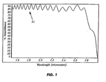
- Fig. 1 is a graph of measured percentage transmission vs. wavelength for a 16 ⁇ m thick polyamide film which shows interference fringes.
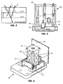
- Fig. 2 shows a basic concept diagram of a light wave passing through a thin film with thickness d.
- Fig. 3 shows a source assembly of the infrared film thickness measurement system according to the invention.
- Fig. 4 shows a receiver assembly according to the invention.
- Fig. 5 shows channels mounted to the center column of the receiver assembly.
- Fig. 6 shows the interference fringes formed from measuring 5 ⁇ m and 16 ⁇ m NYLON films.
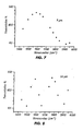
- Fig. 7 depicts a graph plotting the data obtained from measuring a 5 ⁇ m NYLON film.
- Fig. 8 depicts a graph plotting the data obtained from measuring a 16 ⁇ m NYLON film.
- Fig. 9 shows the result of curve fitting calculations for the data depicted in Fig. 8.
- Fig. 10 shows the result of curve fitting calculations for the data depicted in Fig. 9.
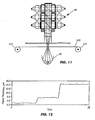
- Fig. 11 shows a schematic drawing of the system adapted to measure moving webs.
- Fig. 12 shows an exemplary graph plotting changes in measured thickness over time in a moving web.
- a novel infrared (IR) film thickness measurement system is provided.
- the invention provides a novel method of extending the capability of IR sensors to measure thin films through configuring multiple detection channels with appropriately chosen filters.
- the characteristic signature of interference fringes can be detected simultaneously with or instead of absorption-based measurements.
- the system comprises three main sections: (i) a source of modulated IR energy, (ii) a sample cell in which the IR energy interacts with the sample to be measured, and (iii) a receiver/analyzer in which the transmitted energy on all of the selected channels is simultaneously read.
- Fig. 3 illustrates an IR source assembly 40.
- An IR source transmits pulses of wideband IR to the sample between the upper and lower heads. It consists of an incandescent light 41, a mirror 42, and supporting hardware for modulating the IR energy.
- a quartz tungsten halogen lamp is used because of its compact size, and the quartz envelope is transparent to the IR energy in the wavebands of interest in the application. The small filament of the lamp makes it possible to focus most of the energy onto the window. Radiation from the quartz tungsten halogen lamp is focused at a light pipe by the mirror 42. The only adjustment required is the focusing of the lamp by sliding it in the holder to maximize the signal strength at the receiver.
- the IR energy is modulated with chopper 43, a lightweight rotating stainless steel disc with preferably eight evenly spaced holes. It is driven by a brushless DC motor 44 that modulates the radiation at 620 ⁇ 25Hz. Modulating the IR energy will prevent the signal received by the detectors in the receiver from being obscured by ambient light or by low frequency noise generated in the detector.
- the sample cell is the located in the space between the IR source and receiver windows.
- the sample film to be measured is placed here to interact with the IR energy. It is very important that the IR energy transmitted be determined only by the properties of the sample and not by extraneous effects, such as dirt and head misalignment or separation.
- the receiver assembly 50 is shown in Fig. 4.
- the function of the receiver is to simultaneously read the transmitted energy in all of the selected bands. This is done by using beamsplitters (66 in Fig. 5) to separate the energy into a series of parallel beams. Each beam is then passed through a filter designed to pass a predetermined waveband, and the total energy in that band is detected by a photoconductive detector.
- the detectors can be chosen from lead sulfide (PbS), lead selenide (PbSe) or silicon (Si) types. Each detector has its own conventional electronics 57 that amplify the received signal, convert it to DC, and transmit it to the receiver.
- the receiver assembly 50 has capacity to support up to preferably twelve channels, and can load additional channels as needed.
- a central aluminum 51 column has sockets 55 that can support up to twelve channels.
- the central column 51 is mounted to a water-cooled plate in the ceiling (not shown) for cooling the sensors.
- Fig. 5 shows channels mounted to the center column 65. In the diagram, only 6 channels are shown mounted for clarity. Additional channels can be mounted to the central column 51 at sockets 55 as required. Each channel comprises a detector 63 an IR band selection filter 67, lens 68 and support electronics. In accordance with an embodiment of the invention, up to preferably twelve channels are utilized at once. Heat from the electronics and peltier cooling of detectors is conducted from the detector assemblies through the column 55 to the water-cooled plate.
- a thin film sample 69 is loaded and secured in the sample cell, and the IR source 40 operated to transmit pulses of wideband IR through the sample.
- the receiver reads the transmitted energy in all of the selected bands simultaneously, and the output of each of the detectors is transmitted to the signal processing circuitry 45 (FIG. 3, 4) to process the signal.
- the wavelength and transmittance percentage can then be electronically plotted on a graph.
- Fig. 6 shows the interference fringes formed from measuring 5 and 16 ⁇ m NYLON films with a Fourier Transform Infrared (FTIR) spectrometer.
- FTIR Fourier Transform Infrared
- appropriately chosen optical filters are utilized.
- the dashed areas under the fringes represents proposed filter wavelengths for a twelve channel IR sensor according to an embodiment of the invention.
- narrow bandpass optical filters will be used. These filters are typically interference filters that have a spectral transmission band surrounded by two blocking bands that allow only a portion of the spectrum to pass. This results in high transmission centered around the chosen wavelength. Optical filters available from Spectrogon US Inc., Parsippany, N.J. are suitable.
- the channels of the IR sensor need to be calibrated for the spectral region where the chosen photoconductive detectors are sensitive to the incident light.
- the type of photo-sensitive element PbS, PbSe or Si
- PbS and Si detectors the total working spectral range of the IRPlus sensor is from 400 nm to 5000 nm.
- PbS detector cells are preferred.
- PbS dedector cells have a spectral sensitivity range from 1000 nm to 3000 nm. For the spectral region between 1600nm and 1800nm, most plastic films do not exhibit absorption lines, or only exhibit weak ones. This is important for the generation of measurable interference fringes.
- the filters for each channel should transmit as narrow band as possible in order to attribute the signal from the IR detector to a single wavelength. This wavelength will be used in the sine wave recovery algorithm discussed below.
- the third requirement arises from the fact that at least half a period (P) is required in order to recover the shape of the interference fringe.
- P the thinner the film, the wider the period of the spectral fringes.
- CWL transmission band central wavelengths
- thicker films require at least three measurement points for each half period of a fringe in order to find an unique solution in the fitting algorithm.
- the twelve filters chosen have CWLs that range from 1620 nm to 1840 nm.
- the filters' characteristics are shown in Table 1.
- the halfwidth (HW) of the filters' transmission bands are shown on Fig. 6 as the shaded areas.
- the following table lists chosen filters from Spectrogon Inc. Table I Filter p/n CWL, nm HW, nm 1.
- NB-1560-009-B 1560 9 2.
- NB-1620-010-B 1620 10 3.
- NB-1630-010-B 1630 10 4.
- NB-1640-010-B 1640 10 5.
- NB-1650-010-B 1650 10 6.
- NB-1680-010-B 1680 10
- NB-1690-010-B 1690 10 8.
- NB-1710-010-B 1710 10 9. NB-1720-010-B 1720 10 10. NB-1730-010-B 1730 10 11. NB-1740-010-B 1740 10 12. NB-1765-010-B 1765 10 13. NB-1775-010-B 1775 10 14. NB-1790-010-B 1790 10 15. NB-1805-010-B 1805 10 16. NB-1820-010-B 1820 10 17. NB-1840-010-B 1840 10 18. NB-1875-010-B 1875 10 19. NB-1905-010-B 1905 10 20. NB-1930-010-B 1930 10 21. NB-1940-010-B 1940 10
- Chi ⁇ 2 represents goodness of the fit. Parameters obtained from the fit can be compared if the parameters of the fringes measured using FTIR spectrometer. The simulations confirm the first possibility of using pre fitting procedure to completely recover the full shape of the spectral fringes using the signal amplitude at just twelve spectral positions. Figs. 9 and 10 show the results of the fitting routine calculations.
- IR-Plus Infrared Transmission Sensor can be modified for use in the IR film thickness measurement system describe above.
- the IR-Plus sensor can be adapted to use up to twelve receiver channels at once. The twelve channels may require calibration before taking measurements, depending on whether the refraction index of the measured film is known. During this procedure a number of film samples should be measured in order to determine the correct refraction index to be used in the formula above.
- the multichannel sensor can be employed to measure film characteristics in a traditional absorptive mode to obtain preliminary approximate values before proceeding with employing the technique described above of measuring the shape of the interference fringes in the transmission spectra.
- fewer than twelve channels, e.g., two channels, of the multichannel infrared sensor can be dedicated to absorptive measurements and the remaining channels can be employed for interference measurements.
- the thin thickness measurement system described above can be adapted for use in paper or other flat-sheet production processes.
- the IR sensor can be adapted to scan across a moving web to detect defects and to measure basis weight and thickness parameters.
- Fig. 11 shows a schematic diagram of such a system, with the web 120 to be measured placed on a conveyer 121 which moves the web past the IR source 40 and the receiver assembly 50.
- the IR source and receiver assembly can be made to be movable in synchronization with each other. Changes in the measured thickness can be depicted in a graph that plots measured thickness versus time.
- the effective thickness can be measured instead. Using the methods described above, the thickness profiles of the web is taken at two chosen spots along the web. The effective thickness is the mean of the difference between the two measured values. The basis weight can then be calculated from the known weight of the sample ream and the measured effective thickness of the paper.
Landscapes
- Physics & Mathematics (AREA)
- General Physics & Mathematics (AREA)
- Length Measuring Devices By Optical Means (AREA)
Claims (10)
- Procédé d'analyse des caractéristiques d'un film comprenant les étapes suivantes :(a) émission d'une faisceau sonde de rayonnement (40, 41, 42, 43, 44),(b) transmission dudit faisceau sonde à travers un film (69) à mesurer,(c) séparation du faisceau transmis à travers le film (69) en une pluralité de faisceaux parallèles avec des diviseurs de faisceau (66),(d) passage de chaque faisceau parallèle à travers un filtre individuel (67) conçu pour passer une gamme d'ondes prédéterminée,(e) détection et enregistrement de l'énergie transmise dans chaque gamme d'ondes prédéterminée avec un détecteur photoconducteur (57, 63),(f) utilisation des données (45) de l'énergie transmise auxdites gammes d'ondes prédéterminées dans un algorithme d'ajustement de courbes afin de récupérer la courbe complète de franges spectrales, et(g) utilisation d'un procédé de comptage de franges afin de calculer les caractéristiques du film (69).
- Procédé selon la revendication 1, dans lequel le filtre (67) est un filtre passe-gamme.
- Procédé selon la revendication 1, dans lequel le filtre (67) est un filtre passe-gamme étroit.
- Procédé selon la revendication 1, dans lequel les énergies transmises dans toutes les gammes d'ondes sélectionnées sont lues simultanément.
- Procédé selon la revendication 1, dans lequel au moins deux filtres (67) de différentes gammes d'ondes sont utilisés.
- Procédé selon la revendication 1, dans lequel la caractéristique mesurée est une épaisseur du film.
- Système d'analyse des caractéristiques d'un film comprenant :un moyen pour émettre un faisceau sonde de rayonnement (40, 41, 42, 43, 44) à travers un film (69) à mesurer,un moyen pour séparer le faisceau (66) transmis à travers le film (69) en une pluralité de faisceaux parallèles,une pluralité de filtres (67), chacun desdits filtres permettant à un faisceau parallèle de passer à une gamme d'ondes prédéterminée,un moyen de détection photoconducteur (57, 63) pour détecter et enregistrer l'énergie transmise dans chaque gamme d'ondes prédéterminée,un moyen électronique (45) pour utiliser les données d'énergie transmise auxdites gammes d'ondes prédéterminées dans un algorithme d'ajustement de courbes afin de récupérer la courbe complète de franges spectrales, et utiliser un procédé de comptage de franges afin de calculer les caractéristiques du film (69).
- Système selon la revendication 7, dans lequel les filtres (67) sont des filtres passe-gamme.
- Système selon la revendication 7, dans lequel les filtres (67) sont des filtres passe-gamme étroits.
- Système selon la revendication 7, dans lequel les énergies transmises dans toutes les gammes d'ondes sélectionnées sont lues simultanément.
Applications Claiming Priority (2)
| Application Number | Priority Date | Filing Date | Title |
|---|---|---|---|
| US10/831,074 US7088456B2 (en) | 2004-04-24 | 2004-04-24 | Thin film thickness measurement using multichannel infrared sensor |
| PCT/US2005/014075 WO2005106387A1 (fr) | 2004-04-24 | 2005-04-22 | Mesure de l'epaisseur d'une couche mince au moyen d'un capteur infrarouge multicanaux |
Publications (2)
| Publication Number | Publication Date |
|---|---|
| EP1740904A1 EP1740904A1 (fr) | 2007-01-10 |
| EP1740904B1 true EP1740904B1 (fr) | 2007-10-24 |
Family
ID=34967273
Family Applications (1)
| Application Number | Title | Priority Date | Filing Date |
|---|---|---|---|
| EP05740132A Expired - Lifetime EP1740904B1 (fr) | 2004-04-24 | 2005-04-22 | Mesure de l'epaisseur d'une couche mince au moyen d'un capteur infrarouge multicanaux |
Country Status (6)
| Country | Link |
|---|---|
| US (1) | US7088456B2 (fr) |
| EP (1) | EP1740904B1 (fr) |
| JP (1) | JP4664971B2 (fr) |
| CA (1) | CA2563777C (fr) |
| DE (1) | DE602005003020T2 (fr) |
| WO (1) | WO2005106387A1 (fr) |
Families Citing this family (15)
| Publication number | Priority date | Publication date | Assignee | Title |
|---|---|---|---|---|
| JP2007123687A (ja) * | 2005-10-31 | 2007-05-17 | Tokyo Seimitsu Co Ltd | 半導体ウェーハ裏面の研削方法及び半導体ウェーハ研削装置 |
| US7382456B2 (en) * | 2005-12-29 | 2008-06-03 | Honeywell Asca, Inc. | Spectroscopic sensor for measuring sheet properties |
| FR2904421B1 (fr) * | 2006-07-28 | 2008-10-31 | Areva Np Sas | Procede de caracterisation non destructif, notammenent pour les particules de combustible nucleaire pour reacteur a haute temperature |
| ES2419165T3 (es) * | 2007-08-13 | 2013-08-19 | Ndc Infrared Engineering Limited | Método y aparato para la detección electromagnética para su uso en la fabricación de una lámina fibrosa |
| US11162893B2 (en) | 2009-06-04 | 2021-11-02 | Pietro Fiorentini S.P.A. | Device and method for determining the composition of a mixture of fluids |
| GB0909662D0 (en) | 2009-06-04 | 2009-07-22 | Cambridge Consultants | Device and method for determining the composition of a mixture of fluids |
| JP5600538B2 (ja) * | 2010-09-24 | 2014-10-01 | 富士フイルム株式会社 | 光学フィルムの膜厚測定方法、及び光学フィルムの製造方法 |
| DE102012019433A1 (de) * | 2012-10-04 | 2014-04-24 | Krohne Optosens Gmbh | Vorrichtung zur Bestimmung einer Kenngröße eines Mediums |
| US9581433B2 (en) | 2013-12-11 | 2017-02-28 | Honeywell Asca Inc. | Caliper sensor and method using mid-infrared interferometry |
| CN108351306A (zh) * | 2015-10-28 | 2018-07-31 | 应用材料公司 | 用以处理基板上的材料的设备、用于处理设备的冷却配置、和用以测量于基板上处理的材料的性质的方法 |
| JP6512361B1 (ja) * | 2018-11-29 | 2019-05-15 | 横河電機株式会社 | 測定装置、測定方法、および測定プログラム |
| WO2020150035A1 (fr) * | 2019-01-14 | 2020-07-23 | Agr International, Inc. | Procédé et appareil d'inspection d'articles transparents creux remplis de liquide |
| US11684253B2 (en) * | 2019-04-24 | 2023-06-27 | Topcon Corporation | 2D multi-layer thickness measurement with reconstructed spectrum |
| DE102020003975A1 (de) | 2020-07-02 | 2022-01-05 | Cellcentric Gmbh & Co. Kg | Verfahren zum Erfassen des Übergangs von zwei miteinander nicht bündig verbundenen Einzelschichten |
| CN116821634B (zh) * | 2023-08-03 | 2026-03-31 | 山西航天清华装备有限责任公司 | 一种工业胶片特性曲线数学模型的优化方法 |
Family Cites Families (13)
| Publication number | Priority date | Publication date | Assignee | Title |
|---|---|---|---|---|
| US4293224A (en) * | 1978-12-04 | 1981-10-06 | International Business Machines Corporation | Optical system and technique for unambiguous film thickness monitoring |
| DE2910673C2 (de) * | 1979-03-19 | 1985-08-08 | Paul Lippke Gmbh & Co Kg, 5450 Neuwied | Verfahren zum berührungslosen Messen des absoluten Gehaltes eines Stoffes(Beisubstanz) in einer die Form eines dünnen Filmes aufweisenden Mischung(Hauptsubstanz und Beisubstanz) mehrerer Stoffe, insbesondere zum Messen des absoluten Gehaltes von Wasser in Papier |
| US4928013A (en) * | 1987-02-17 | 1990-05-22 | Measurex Corporation | Temperature insensitive moisture sensor |
| JPH04131704A (ja) * | 1990-09-25 | 1992-05-06 | Hitachi Electron Eng Co Ltd | 磁気ヘッド浮上量の動特性測定方法 |
| DE69232697T2 (de) * | 1991-12-09 | 2003-02-06 | Measurex Corp., Cupertino | Sensor und methode zur messung ausgewählter bestandteile eines materials |
| JP2866559B2 (ja) * | 1993-09-20 | 1999-03-08 | 大日本スクリーン製造株式会社 | 膜厚測定方法 |
| US5798837A (en) | 1997-07-11 | 1998-08-25 | Therma-Wave, Inc. | Thin film optical measurement system and method with calibrating ellipsometer |
| JP3819187B2 (ja) * | 1999-09-28 | 2006-09-06 | 富士写真フイルム株式会社 | マルチバンド画像の分光反射率のスペクトル推定方法およびスペクトル推定システム |
| US6459488B1 (en) | 2000-02-10 | 2002-10-01 | The United States Of America As Represented By The Secretary Of The Navy | Diffuse reflectance method and apparatus for determining thickness of an infrared translucent layer |
| US6281678B1 (en) | 2000-02-29 | 2001-08-28 | Gene R Auville | Tri-tip probe |
| US6573999B1 (en) | 2000-07-14 | 2003-06-03 | Nanometrics Incorporated | Film thickness measurements using light absorption |
| US6556306B2 (en) | 2001-01-04 | 2003-04-29 | Rensselaer Polytechnic Institute | Differential time domain spectroscopy method for measuring thin film dielectric properties |
| US6646752B2 (en) | 2002-02-22 | 2003-11-11 | Taiwan Semiconductor Manufacturing Co. Ltd | Method and apparatus for measuring thickness of a thin oxide layer |
-
2004
- 2004-04-24 US US10/831,074 patent/US7088456B2/en not_active Expired - Lifetime
-
2005
- 2005-04-22 WO PCT/US2005/014075 patent/WO2005106387A1/fr not_active Ceased
- 2005-04-22 DE DE602005003020T patent/DE602005003020T2/de not_active Expired - Lifetime
- 2005-04-22 EP EP05740132A patent/EP1740904B1/fr not_active Expired - Lifetime
- 2005-04-22 JP JP2007509711A patent/JP4664971B2/ja not_active Expired - Fee Related
- 2005-04-22 CA CA2563777A patent/CA2563777C/fr not_active Expired - Fee Related
Also Published As
| Publication number | Publication date |
|---|---|
| WO2005106387A1 (fr) | 2005-11-10 |
| US7088456B2 (en) | 2006-08-08 |
| DE602005003020D1 (de) | 2007-12-06 |
| CA2563777A1 (fr) | 2005-11-10 |
| CA2563777C (fr) | 2012-03-20 |
| JP4664971B2 (ja) | 2011-04-06 |
| DE602005003020T2 (de) | 2008-08-14 |
| EP1740904A1 (fr) | 2007-01-10 |
| JP2007534945A (ja) | 2007-11-29 |
| US20050237539A1 (en) | 2005-10-27 |
Similar Documents
| Publication | Publication Date | Title |
|---|---|---|
| EP1740904B1 (fr) | Mesure de l'epaisseur d'une couche mince au moyen d'un capteur infrarouge multicanaux | |
| US5124552A (en) | Sensor and method for measuring web moisture with optimal temperature insensitivity over a wide basis weight range | |
| US3822098A (en) | Multispectral sensor means measuring depolarized radiation | |
| EP2815206B1 (fr) | Mesure de l'épaisseur de revêtement sur bande non-uniforme continue à l'aide de détecteur de térahertz (thz) | |
| EP2106537B1 (fr) | Spectromètre et procédé pour commander le spectromètre | |
| US4302108A (en) | Detection of subsurface defects by reflection interference | |
| EP0279743B1 (fr) | Capteur d'humidité à compensation de température | |
| US4966455A (en) | Real time mottle measuring device and method | |
| US9024259B2 (en) | Method and apparatus for electromagnetic detection for use in the manufacture of fibrous web | |
| US6281498B1 (en) | Infrared measuring gauges | |
| EP3341703B1 (fr) | Verres à l'oxyde d'holmium comme standards d'étalonnage pour capteurs d'humidité dans l'infrarouge proche | |
| JP6985461B2 (ja) | 複合シートの重量の測定用の作業中のグレード選択 | |
| EP2480877B1 (fr) | Procédé et appareil de mesure en ligne d'une propriété d'une bande continue | |
| US7868295B2 (en) | Advanced calorimetric spectroscopy for commercial applications of chemical and biological sensors | |
| US6495831B1 (en) | Method and apparatus for measuring properties of paper | |
| US20110206830A1 (en) | Reverse interferometric method and apparatus for measuring layer thickness | |
| JPH11237377A (ja) | 紙やシートの品質測定装置 | |
| US5506407A (en) | High resolution high speed film measuring apparatus and method | |
| US20050244093A1 (en) | Wavelength-tuned intensity measurement of surface plasmon resonance sensor | |
| JPS60224002A (ja) | 赤外線厚み計 | |
| WO1999041590A1 (fr) | Procede et dispositif de mesure de la quantite de revetement sur un substrat en mouvement | |
| JPH08254502A (ja) | 鋼材のスケール性状測定方法及び装置 | |
| Kravetz | Dual-Beam Double Pass Optical Sensor For On-Line Web Transmission Measurements | |
| Znamensky et al. | Express indicator of ecological situations |
Legal Events
| Date | Code | Title | Description |
|---|---|---|---|
| PUAI | Public reference made under article 153(3) epc to a published international application that has entered the european phase |
Free format text: ORIGINAL CODE: 0009012 |
|
| 17P | Request for examination filed |
Effective date: 20061103 |
|
| AK | Designated contracting states |
Kind code of ref document: A1 Designated state(s): DE FI FR GB SE |
|
| RIN1 | Information on inventor provided before grant (corrected) |
Inventor name: AXELROD, STEVE Inventor name: GERMANENKO, IGOR, N. |
|
| GRAP | Despatch of communication of intention to grant a patent |
Free format text: ORIGINAL CODE: EPIDOSNIGR1 |
|
| RBV | Designated contracting states (corrected) |
Designated state(s): DE FI FR GB SE |
|
| DAX | Request for extension of the european patent (deleted) | ||
| GRAS | Grant fee paid |
Free format text: ORIGINAL CODE: EPIDOSNIGR3 |
|
| GRAA | (expected) grant |
Free format text: ORIGINAL CODE: 0009210 |
|
| AK | Designated contracting states |
Kind code of ref document: B1 Designated state(s): DE FI FR GB SE |
|
| REG | Reference to a national code |
Ref country code: GB Ref legal event code: FG4D |
|
| REF | Corresponds to: |
Ref document number: 602005003020 Country of ref document: DE Date of ref document: 20071206 Kind code of ref document: P |
|
| REG | Reference to a national code |
Ref country code: SE Ref legal event code: TRGR |
|
| EN | Fr: translation not filed | ||
| PLBE | No opposition filed within time limit |
Free format text: ORIGINAL CODE: 0009261 |
|
| STAA | Information on the status of an ep patent application or granted ep patent |
Free format text: STATUS: NO OPPOSITION FILED WITHIN TIME LIMIT |
|
| 26N | No opposition filed |
Effective date: 20080725 |
|
| PG25 | Lapsed in a contracting state [announced via postgrant information from national office to epo] |
Ref country code: FR Free format text: LAPSE BECAUSE OF FAILURE TO SUBMIT A TRANSLATION OF THE DESCRIPTION OR TO PAY THE FEE WITHIN THE PRESCRIBED TIME-LIMIT Effective date: 20080808 |
|
| EUG | Se: european patent has lapsed | ||
| PG25 | Lapsed in a contracting state [announced via postgrant information from national office to epo] |
Ref country code: SE Free format text: LAPSE BECAUSE OF NON-PAYMENT OF DUE FEES Effective date: 20080423 |
|
| PGFP | Annual fee paid to national office [announced via postgrant information from national office to epo] |
Ref country code: FI Payment date: 20180420 Year of fee payment: 14 |
|
| PGFP | Annual fee paid to national office [announced via postgrant information from national office to epo] |
Ref country code: DE Payment date: 20190430 Year of fee payment: 15 |
|
| PGFP | Annual fee paid to national office [announced via postgrant information from national office to epo] |
Ref country code: GB Payment date: 20190429 Year of fee payment: 15 |
|
| PG25 | Lapsed in a contracting state [announced via postgrant information from national office to epo] |
Ref country code: FI Free format text: LAPSE BECAUSE OF NON-PAYMENT OF DUE FEES Effective date: 20190422 |
|
| REG | Reference to a national code |
Ref country code: DE Ref legal event code: R119 Ref document number: 602005003020 Country of ref document: DE |
|
| PG25 | Lapsed in a contracting state [announced via postgrant information from national office to epo] |
Ref country code: DE Free format text: LAPSE BECAUSE OF NON-PAYMENT OF DUE FEES Effective date: 20201103 |
|
| GBPC | Gb: european patent ceased through non-payment of renewal fee |
Effective date: 20200422 |
|
| PG25 | Lapsed in a contracting state [announced via postgrant information from national office to epo] |
Ref country code: GB Free format text: LAPSE BECAUSE OF NON-PAYMENT OF DUE FEES Effective date: 20200422 |