EP1742893B1 - Dispositifs de formation de motifs composites pour lithographie molle - Google Patents
Dispositifs de formation de motifs composites pour lithographie molle Download PDFInfo
- Publication number
- EP1742893B1 EP1742893B1 EP05756327A EP05756327A EP1742893B1 EP 1742893 B1 EP1742893 B1 EP 1742893B1 EP 05756327 A EP05756327 A EP 05756327A EP 05756327 A EP05756327 A EP 05756327A EP 1742893 B1 EP1742893 B1 EP 1742893B1
- Authority
- EP
- European Patent Office
- Prior art keywords
- polymer layer
- layer
- contact
- composite
- polymer
- Prior art date
- Legal status (The legal status is an assumption and is not a legal conclusion. Google has not performed a legal analysis and makes no representation as to the accuracy of the status listed.)
- Expired - Lifetime
Links
Images











Classifications
-
- B—PERFORMING OPERATIONS; TRANSPORTING
- B82—NANOTECHNOLOGY
- B82Y—SPECIFIC USES OR APPLICATIONS OF NANOSTRUCTURES; MEASUREMENT OR ANALYSIS OF NANOSTRUCTURES; MANUFACTURE OR TREATMENT OF NANOSTRUCTURES
- B82Y10/00—Nanotechnology for information processing, storage or transmission, e.g. quantum computing or single electron logic
-
- C—CHEMISTRY; METALLURGY
- C04—CEMENTS; CONCRETE; ARTIFICIAL STONE; CERAMICS; REFRACTORIES
- C04B—LIME, MAGNESIA; SLAG; CEMENTS; COMPOSITIONS THEREOF, e.g. MORTARS, CONCRETE OR LIKE BUILDING MATERIALS; ARTIFICIAL STONE; CERAMICS; REFRACTORIES; TREATMENT OF NATURAL STONE
- C04B24/00—Use of organic materials as active ingredients for mortars, concrete or artificial stone, e.g. plasticisers
- C04B24/24—Macromolecular compounds
- C04B24/38—Polysaccharides or derivatives thereof
- C04B24/383—Cellulose or derivatives thereof
-
- B—PERFORMING OPERATIONS; TRANSPORTING
- B81—MICROSTRUCTURAL TECHNOLOGY
- B81C—PROCESSES OR APPARATUS SPECIALLY ADAPTED FOR THE MANUFACTURE OR TREATMENT OF MICROSTRUCTURAL DEVICES OR SYSTEMS
- B81C1/00—Manufacture or treatment of devices or systems in or on a substrate
- B81C1/00436—Shaping materials, i.e. techniques for structuring the substrate or the layers on the substrate
- B81C1/00444—Surface micromachining, i.e. structuring layers on the substrate
- B81C1/0046—Surface micromachining, i.e. structuring layers on the substrate using stamping, e.g. imprinting
-
- B—PERFORMING OPERATIONS; TRANSPORTING
- B82—NANOTECHNOLOGY
- B82Y—SPECIFIC USES OR APPLICATIONS OF NANOSTRUCTURES; MEASUREMENT OR ANALYSIS OF NANOSTRUCTURES; MANUFACTURE OR TREATMENT OF NANOSTRUCTURES
- B82Y40/00—Manufacture or treatment of nanostructures
-
- C—CHEMISTRY; METALLURGY
- C04—CEMENTS; CONCRETE; ARTIFICIAL STONE; CERAMICS; REFRACTORIES
- C04B—LIME, MAGNESIA; SLAG; CEMENTS; COMPOSITIONS THEREOF, e.g. MORTARS, CONCRETE OR LIKE BUILDING MATERIALS; ARTIFICIAL STONE; CERAMICS; REFRACTORIES; TREATMENT OF NATURAL STONE
- C04B28/00—Compositions of mortars, concrete or artificial stone, containing inorganic binders or the reaction product of an inorganic and an organic binder, e.g. polycarboxylate cements
- C04B28/14—Compositions of mortars, concrete or artificial stone, containing inorganic binders or the reaction product of an inorganic and an organic binder, e.g. polycarboxylate cements containing calcium sulfate cements
-
- G—PHYSICS
- G03—PHOTOGRAPHY; CINEMATOGRAPHY; ANALOGOUS TECHNIQUES USING WAVES OTHER THAN OPTICAL WAVES; ELECTROGRAPHY; HOLOGRAPHY
- G03F—PHOTOMECHANICAL PRODUCTION OF TEXTURED OR PATTERNED SURFACES, e.g. FOR PRINTING, FOR PROCESSING OF SEMICONDUCTOR DEVICES; MATERIALS THEREFOR; ORIGINALS THEREFOR; APPARATUS SPECIALLY ADAPTED THEREFOR
- G03F7/00—Photomechanical, e.g. photolithographic, production of textured or patterned surfaces, e.g. printing surfaces; Materials therefor, e.g. comprising photoresists; Apparatus specially adapted therefor
- G03F7/0002—Lithographic processes using patterning methods other than those involving the exposure to radiation, e.g. by stamping
-
- B—PERFORMING OPERATIONS; TRANSPORTING
- B82—NANOTECHNOLOGY
- B82Y—SPECIFIC USES OR APPLICATIONS OF NANOSTRUCTURES; MEASUREMENT OR ANALYSIS OF NANOSTRUCTURES; MANUFACTURE OR TREATMENT OF NANOSTRUCTURES
- B82Y30/00—Nanotechnology for materials or surface science, e.g. nanocomposites
-
- C—CHEMISTRY; METALLURGY
- C04—CEMENTS; CONCRETE; ARTIFICIAL STONE; CERAMICS; REFRACTORIES
- C04B—LIME, MAGNESIA; SLAG; CEMENTS; COMPOSITIONS THEREOF, e.g. MORTARS, CONCRETE OR LIKE BUILDING MATERIALS; ARTIFICIAL STONE; CERAMICS; REFRACTORIES; TREATMENT OF NATURAL STONE
- C04B2111/00—Mortars, concrete or artificial stone or mixtures to prepare them, characterised by specific function, property or use
- C04B2111/00034—Physico-chemical characteristics of the mixtures
- C04B2111/00181—Mixtures specially adapted for three-dimensional printing (3DP), stereo-lithography or prototyping
Definitions
- Photolithography is currently the most prevalent method of microfabrication, and nearly all integrated electronic circuits are made using this technique.
- conventional projection mode photolithography an optical image corresponding to a selected two dimensional pattern is generated using a photomask. The image is optically reduced and projected onto a thin film of photoresist spin coated onto a substrate.
- Direct Write to Wafer photolithographic techniques a photoresist is directly exposed to laser light, an electron beam or ion beam without the use of a photomask. Interaction between light, electrons and/or ions and molecules comprising the photoresist chemically alters selected regions of the photoresist in a manner enabling fabrication of structures having well defined physical dimensions.
- Photolithography is exceptionally well suited for generating two-dimensional distributions of features on flat surfaces.
- photolithography is capable of generating more complex three dimensional distributions of features on flat surfaces using additive fabrication methods involving formation of multilayer stacks.
- the methods, devices and device components are capable of generating patterns comprising a wide range of materials including, but not limited to, metals, organic compounds, inorganic compounds, colloidal materials, suspensions, biological molecules, cells, polymers, microstructures, nanostructures and salt solutions.
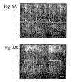
- FIGs. 6A and 6B show top view optical micrographs that illustrate the reduced tendency for sagging of recessed areas in a composite stamp.
- Figure 6A corresponds to a conventional single layer PDMS stamp and
- Figure 6B corresponds to a composite stamp.
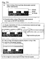
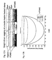
- Fig. 7 shows the extent of shrinkage observed after curing a four layer composite stamp comprising a first PDMS layer, a second polyimide layer, a third PDMS layer and a fourth polyimide layer.
- Elastomers useful in the present invention may include, but are not limited to, silicon containing polymers such as polysiloxanes including poly(dimethyl siloxane) (i.e PDMS and h-PDMS), poly(methyl siloxane), partially alkylated poly(methyl siloxane), poly(alkyl methyl siloxane) and poly(phenyl methyl siloxane), silicon modified el;astomers, thermoplastic elastomers, styrenic materials, olefenic materials, polyolefin, polyurethane thermoplastic elastomers, polyamides, synthetic rubbers, polyisobutylene, poly(styrene-butadiene-styrene), polyurethanes, polychloroprene and silicones.
- silicon containing polymers such as polysiloxanes including poly(dimethyl siloxane) (i.e PDMS and h-PDMS), poly(methyl siloxane),
- PDMS Sylgard 184 from Dow Coming
- h-PDMS VDT-731, Gelest Corp
- curing of 184 PDMS may be performed at room temperature using extra amounts of curing agent.
- First polymer layers comprising PDMS or h-PDMS are preferably cured in the presence of the second high modulus layer, such as a polyimide layer, to reduce shrinkage induced by curing and/or polymerization.
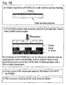
- a four layer composite patterning device 600 shown schematically in Figure 10 , was evaluated comprising a first 5 micron thick PDMS polymer layer 610 , a second 25 micron polyimide (Kapton ®) polymer layer 620 , a third 5 micron thick PDMS polymer layer 630 and a fourth 25 micron polyimide (Kapton ®) polymer layer 640 .
- a two layer composite patterning device 700 shown schematically in Figure 11A was evaluated comprising a first 5 micron thick PDMS polymer layer 710 , a second 25 micron polyimide (Kapton ®) polymer layer 720 .
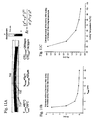
- FIGs. 13A-C shows the results of a computational study of horizontal distortion due to thermal/chemical shrinkage during polymerization for a two layer composite stamp of the present invention.
- Figure 13A is a schematic illustrating a two layer composite stamp comprising a PDMS layer of variable thickness operationally coupled to a 25 micron Kapton layer.
- Figure 13B is a plot of the predicted horizontal distortion as a function of the thickness of the PDMS first layer in microns.
- Figure 13C is a plot of the predicted horizontal distortion as a function of the distance along the external surface of the PDMS first layer in millimeters.
- the modeling results suggest that the magnitude of distortions in planes parallel to the contact surfaces on the external surface of the PDMS first layer due to polymerization is directly proportional to the PDMS first layer thickness.
- the modeling results show that distortions in planes parallel to the contact surfaces on the external surface of the PDMS first layer due to polymerization are largely confined to the edges of the stamp when the thickness of the PDMS first layer is decreased.
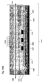
- the fiber reinforced composite stamp 900 comprises a first layer 905 comprising PDMS and having a relief pattern with relief features of selected physical dimensions, a second layer 910 comprising a composite polymer having an array of fine glass fibers in a first selected orientation, a third layer 915 comprising a composite polymer having a mesh of larger glass fibers in a second selected orientation, a fourth layer 920 comprising a composite polymer having a mesh of large glass fibers in a third selected orientation and a fifth layer 925 comprising a composite polymer having an array of fine glass fibers in a fourth selected orientation.
- use of device configurations in the present invention providing a substantially symmetrical distribution of thermal expansion coefficients about layer alignment axis 980 orthogonal to a plane containing the contact surface(s) is useful for providing thermally stable patterning devices that exhibit minimal pattern distortions induced by changes in temperature. Further more, this symmetrical arrangement minimizes relief pattern distortions induced during curing, for example pattern distortions caused of curling of polymer layers during curing.
- SiO 2 exhibits good adhesion to some polymers, including PDMS.
- Carbon fibers are another class of material that integration into polymer layers leads to substantially enhancement of flexural rigidity and Young's modulus while allowing for device flexibility useful for establishing good conformal contact with a range of surface morphologies.
- Fiber materials useful in the present composite patterning devices include, but are not limited to, fibers comprising glass including oxides such as SiO 2 , Al 2 O 2 , B 2 O 3 , CaO, MgO, ZnO, BaO, Li 2 O, TiO 2 , ZrO 2 , Fe 2 O 3 , F 2 , and Na 3 O / K 2 O, carbon, polymers such as aramid fiber and dyneema, metals and ceramics or mixtures of these materials may be incorporated into patterning devices of the present invention.
- Patterning agents of the present invention may provide functionality other than or in addition to facilitating proper alignment of a patterning device and a substrate surface.
- patterning agents of the present invention comprise an optical filtering medium for a photomask of the present invention.
- patterning agents comprise a transfer material that is molded onto a substrate surface, for example a prepolymer material that is molded into a pattern embossed on the substrate surface upon exposure to electromagnetic radiation or upon increasing temperature.
- Patterning agents of the present invention may also provide a multifunctional character such as a combination of facilitating alignment of a contact surface of a patterning device and a substrate surface undergoing processing and providing optical filtering and/or a transfer material for patterning a substrate surface.
- patterning agents of the present invention act as lubricants by reducing friction generated between a mating contact surface and substrate surface pair of an alignment system, such as a lock and key registration system. By reducing friction, the patterning agent allows the patterning device and the substrate to establish conformal contact and move relative to each other, thereby sampling a range of possible relative orientations.
- additional mobility provided by the patterning agent allows the patterning device and substrate surface to realize a stable, selected relative orientation characterized by effective coupling between complementary relief features and recessed regions on the mating surfaces.
- Effective patterning agents facilitate establishing correct registration without interfering with establishment of conformal contact.
- Useful patterning agents include fluids, such as liquids and colloids, thin films and particulate materials. Exemplary patterning agents include Optical Brightener, Benetex OB-EP from Mayzo, Parker ink, Water soluble black wooden dye Powerder from Constantines Wood Center.
- patterning agent 1315 is a material that absorbs, reflects or scatters electromagnetic radiation directed onto photomask 1305 and, therefore, the shapes and physical dimensions of relief features 1308 and recessed regions 1307 establishes two dimensional spatial distributions of intensities, wavelengths and/or polarization states of electromagnetic radiation transmitted to photosensitive layer 1314 on external surface 1313 .
- selected regions of photosensitive layer 1314 may be illuminated with selected intensities of electromagnetic radiation having selected wavelengths and polarization states, and selected regions of photosensitive layer 1314 may be shielded from exposure to electromagnetic radiation having selected wavelengths and polarization states.
Landscapes
- Chemical & Material Sciences (AREA)
- Engineering & Computer Science (AREA)
- Nanotechnology (AREA)
- Ceramic Engineering (AREA)
- Physics & Mathematics (AREA)
- Crystallography & Structural Chemistry (AREA)
- Materials Engineering (AREA)
- General Physics & Mathematics (AREA)
- Structural Engineering (AREA)
- Organic Chemistry (AREA)
- Manufacturing & Machinery (AREA)
- Condensed Matter Physics & Semiconductors (AREA)
- Inorganic Chemistry (AREA)
- Chemical Kinetics & Catalysis (AREA)
- Mathematical Physics (AREA)
- Theoretical Computer Science (AREA)
- Composite Materials (AREA)
- Microelectronics & Electronic Packaging (AREA)
- Shaping Of Tube Ends By Bending Or Straightening (AREA)
- Laminated Bodies (AREA)
- Exposure Of Semiconductors, Excluding Electron Or Ion Beam Exposure (AREA)
Claims (29)
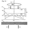
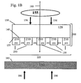
- Un dispositif de formation de motifs composites (100) pour générer un motif sur la surface d'un substrat, se composant de ce qui suit :une première couche polymère (110) comprenant un motif en relief en trois dimensions ayant au moins une surface de contact dessus, la première couche polymère (110) ayant un module d'Young réduit sélectionné dans une plage allant d'environ 1 MPa à environ 10 MPa et ayant une surface interne opposée à la surface de contact ; etune deuxième couche polymère (120) ayant une surface interne et une surface externe ; ladite deuxième couche polymère ayant un module d'Young élevé sélectionné dans une plage allant d'environ 1 GPa à environ 10 GPa ; dans lequel la première couche polymère (110) et la deuxième couche polymère (120) sont disposées de telle sorte qu'une force appliquée sur la surface externe de la deuxième couche polymère (120) est transmise à la première couche polymère (110) ;
dans lequel le dispositif de formation de motifs composites est capable d'établir un contact conforme entre au moins une partie de la surface de contact de la première couche polymère (110) et la surface du substrat. - Le dispositif de la revendication 1, dans lequel la surface interne de la première couche polymère est en contact avec la surface interne de la deuxième couche polymère ou dans lequel la première couche polymère et la deuxième couche polymère sont reliées par une couche de liaison placée entre la surface interne (135) de la première couche polymère et la surface interne (140) de la deuxième couche polymère.
- Le dispositif de la revendication 1, dans lequel la première couche polymère et la deuxième couche polymère sont disposées de telle sorte qu'une force appliquée sur la surface externe de la deuxième couche polymère est transmise à au moins une partie de la surface de contact (130) de la première couche polymère.
- Le dispositif de la revendication 1, dans lequel l'épaisseur de la première couche polymère est sélectionnée dans une plage allant d'environ 1 micron à environ 100 microns.
- Le dispositif de la revendication 1, dans lequel l'épaisseur de la deuxième couche polymère est sélectionnée dans une plage allant d'environ 10 microns à environ 100 microns.
- Le dispositif de la revendication 1, dans lequel le ratio de l'épaisseur de la première couche polymère et l'épaisseur de la deuxième couche polymère est sélectionné dans une plage allant d'environ 1 à environ 10.
- Le dispositif de la revendication 1, dans lequel la deuxième couche polymère est sélectionnée dans le groupe se composant d'une couche thermodurcie, d'un polyimide, d'une couche thermoplastique, d'un matériau contenant des fibres et d'une couche polymère composite.
- Le dispositif de la revendication 1, dans lequel la deuxième couche polymère comprend un polymère ayant un coefficient d'expansion thermique inférieur ou égal à environ 14,5 ppm.
- Le dispositif de la revendication 1, dans lequel la première couche polymère est une couche élastomère, un matériau contenant des fibres ou une couche polymère composite.
- Le dispositif de la revendication 1 comprenant également une troisième couche polymère se trouvant entre les première et deuxième couches polymères, dans lequel le troisième polymère est une couche polymère composite comprenant un matériau en fibres.
- Le dispositif de la revendication 1, dans lequel le dispositif de formation de motifs composites possède une rigidité à la flexion sélectionnée dans la plage allant d'environ 1 x 10⁷ Nm à environ 1 x 10⁻⁵ Nm.
- Le dispositif de la revendication 1, dans lequel la première couche polymère est une couche discontinue, dans lequel le motif en relief en trois dimensions comprend plusieurs éléments en relief indépendants et dans lequel les éléments en relief indépendants sont en contact avec la deuxième couche polymère.
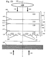
- Le dispositif de la revendication 1 comprenant également une troisième couche polymère (310) ayant une surface interne et une surface externe, dans lequel les première, deuxième et troisième couches polymères sont disposées de telle sorte qu'une force appliquée sur la surface externe de la troisième couche polymère est transmise à la première couche polymère et dans lequel la surface interne de la troisième couche polymère est en contact avec la surface externe de la deuxième couche polymère ou dans lequel les deuxième et troisième couches polymères sont reliées par une couche de liaison se trouvant entre la surface externe de la deuxième couche polymère et la surface interne de la troisième couche polymère.
- Le dispositif de la revendication 13, dans lequel la troisième couche polymère possède un module d'Young réduit sélectionné dans la plage allant d'environ 1 MPa à environ 10 MPa.
- Le dispositif de la revendication 13, dans lequel l'épaisseur de la troisième couche polymère est sélectionnée dans la plage allant d'environ 1 micron à environ 100 microns et représente moins de 10 % environ de l'épaisseur de la première couche polymère ou des deux.
- Le dispositif de la revendication 13, dans lequel le coefficient d'expansion thermique de la première couche polymère représente moins de 10 % environ du coefficient d'expansion thermique de la troisième couche polymère.
- Le dispositif de la revendication 13, dans lequel la troisième couche polymère est une couche élastomérique.
- Le dispositif de la revendication 13 comprenant également une quatrième couche (410) ayant une surface interne et une surface externe, dans lequel les première, deuxième, troisième et quatrième couches polymères sont disposées de telle sorte qu'une force appliquée sur la surface externe de la quatrième couche polymère est transmise à la première couche polymère et dans lequel la surface interne de la quatrième couche polymère est en contact avec la surface externe de la troisième couche polymère ou dans lequel la troisième couche polymère et la quatrième couches polymères sont reliées par une couche de liaison se trouvant entre la surface externe de la troisième couche polymère et la surface interne de la quatrième couche polymère.
- Le dispositif de la revendication 18, dans lequel la quatrième couche polymère possède un module d'Young élevé sélectionné dans une plage allant d'environ 1 GPa à environ 10 GPa.
- Le dispositif de la revendication 18, dans lequel l'épaisseur de la quatrième couche polymère est sélectionnée dans une plage allant d'environ 10 microns à environ 100 microns et représente moins de 10 % environ de l'épaisseur de la deuxième couche polymère ou des deux.
- Le dispositif de la revendication 18, dans lequel le coefficient d'expansion thermique de la quatrième couche polymère représente moins de 10 % environ du coefficient d'expansion thermique de la deuxième couche polymère.
- Le dispositif de la revendication 1 comprenant également un actionneur (155) connecté à la surface externe de la deuxième couche polymère (120), de la troisième couche polymère (310) ou de la quatrième couche polymère (410), dans lequel l'actionneur est capable de fournir une force à la surface externe de la deuxième couche polymère, de la troisième couche polymère ou de la quatrième couche polymère.
- Le dispositif de la revendication 1 comprenant un timbre, un moule ou un masque photographique.
- Le dispositif de la revendication 1, dans lequel le dispositif de formation de motifs composites possède un coefficient d'expansion thermique net représentant moins de 10 % environ du coefficient d'expansion thermique du substrat.
- Le dispositif de la revendication 1 comprenant également une troisième couche (310) ayant une surface interne et une surface externe, dans lequel les première, deuxième et troisième couches polymères sont disposées de telle sorte qu'une force appliquée sur la surface externe de la troisième couche polymère est transmise à la première couche polymère ; et
dans lequel les épaisseurs et coefficients d'expansion thermique des première et troisième couches fournit une distribution sensiblement symétrique des coefficients d'expansion thermique autour du centre du dispositif de formation de motifs le long d'un axe d'alignement de couche passant par ledit dispositif de formation de motifs et dans lequel le dispositif de formation de motifs composites est capable d'établir un contact conforme entre au moins une partie de la surface de contact de la première couche et la surface du substrat. - Un procédé de génération d'un motif sur la surface d'un substrat (180) se composant des opérations suivantes :se procurer un dispositif de formation de motifs composites comprenant :une première couche polymère (110) comportant un motif en relief en trois dimensions ayant au moins une surface de contact dessus, la première couche polymère ayant un module d'Young réduit sélectionné dans une plage allant d'environ 1 MPa à environ 10 MPa et ayant une surface interne opposée à la surface de contact ; etune deuxième couche polymère (120) ayant une surface interne et une surface externe ; la deuxième couche polymère ayant un module d'Young élevé sélectionné dans une plage allant d'environ 1 GPa à 10 GPa ; dans lequel la première couche polymère et la deuxième couche polymère sont disposées de telle sorte qu'une force appliquée sur la surface externe de la deuxième couche polymère est transmise à la première couche polymère ;déposer un matériau de transfert sur la surface de contact de la première couche polymère, ce qui a pour effet de générer une couche de matériau de transfert sur la surface de contact ;mettre en contact le dispositif de formation de motifs composites et la surface du substrat de façon à établir un contact conforme entre au moins une partie de la surface de contact et de la surface du substrat, dans lequel la couche de matériau de transfert est exposée à la surface du substrat ; etséparer le dispositif de formation de motifs composites et la surface du substrat, ce qui a pour effet de transférer au moins une partie du matériau de transfert sur la surface du substrat et de générer le motif sur la surface du substrat.
- Un procédé de génération d'un motif sur la surface d'un substrat (130), le procédé se composant des opérations suivantes :se procurer un dispositif de formation de motifs composites comprenant :une première couche polymère (110) comportant un motif en relief en trois dimensions ayant au moins une surface de contact dessus, la première couche polymère ayant un module d'Young réduit sélectionné dans une plage allant d'environ 1 MPa à environ 10 MPa et ayant une surface interne opposée à la surface de contact ; etune deuxième couche polymère (120) ayant une surface interne et une surface externe ; la deuxième couche polymère ayant un module d'Young élevé sélectionné dans une plage allant d'environ 1 GPa à 10 GPa ; dans lequel la première couche polymère et la deuxième couche polymère sont disposées de telle sorte qu'une force appliquée sur la surface externe de la deuxième couche polymère est transmise à la première couche polymère ;mettre en contact le dispositif de formation de motifs composites et la surface du substrat de façon à établir un contact conforme entre au moins une partie de la surface de contact et de la surface du substrat, et ce faisant générer un moule comprenant l'espace séparant le motif en relief en trois dimensions et la surface du substrat ;introduire un matériau de transfert dans le moule ; etséparer le dispositif de formation de motifs composites et la surface du substrat, ce qui a pour effet de générer le motif sur la surface du substrat.
- Un procédé de génération d'un motif sur la surface d'un substrat (180) comprenant un matériau photosensible, le procédé se composant des opérations suivantes :se procurer un dispositif de formation de motifs composites comprenant :une première couche polymère (110) comportant un motif en relief en trois dimensions ayant au moins une surface de contact dessus, la première couche polymère ayant un module d'Young réduit sélectionné dans une plage allant d'environ 1 MPa à environ 10 MPa et ayant une surface interne opposée à la surface de contact ; etune deuxième couche polymère (120) ayant une surface interne et une surface externe ; la deuxième couche polymère ayant un module d'Young élevé sélectionné dans une plage allant d'environ 1 GPa à 10 GPa ; dans lequel la première couche polymère et la deuxième couche polymère sont disposées de telle sorte qu'une force appliquée sur la surface externe de la deuxième couche polymère est transmise à la première couche polymère ;mettre en contact le dispositif de formation de motifs composites et la surface du substrat de façon à établir un contact conforme entre au moins une partie de la surface de contact et de la surface du substrat ; etdiriger des rayonnements électromagnétiques à travers le dispositif de formation de motifs composites et sur la surface du substrat, ce qui a pour effet de générer un motif de rayonnement électromagnétique ayant une distribution en deux dimensions sélectionnée d'intensités sur la surface du substrat ; dans lequel l'interaction du rayonnement électromagnétique et du matériau sensible aux rayonnements génère des régions chimiquement modifiées de matériau sensible aux rayonnements, ce qui a pour effet de générer le motif sur la surface du substrat.
- Un procédé de fabrication d'un dispositif de formation de motifs composites se composant des opérations suivantes :se procurer un motif en relief maître ayant un motif en relief en trois dimensions sélectionné ;mettre en contact le motif en relief maître avec un prépolymère d'un polymère de module réduit sélectionné dans une plage allant d'environ 1 MPa à environ 10 MPa ;mettre en contact le matériau prépolymère avec une couche polymère de module élevé sélectionné dans une plage allant d'environ 1 GPa à 10 GPa ;polymériser le prépolymère, ce qui a pour effet de générer une couche polymère de module réduit en contact avec la couche polymère de module élevé en contact avec le motif en relief maître ; la couche polymère de module réduit ayant un motif en relief en trois dimensions ; etséparer la couche polymère de module réduit du motif en relief maître, ce qui a pour effet de créer le dispositif de formation de motifs composites.
Applications Claiming Priority (2)
| Application Number | Priority Date | Filing Date | Title |
|---|---|---|---|
| US56560404P | 2004-04-27 | 2004-04-27 | |
| PCT/US2005/014449 WO2005104756A2 (fr) | 2004-04-27 | 2005-04-27 | Dispositifs de formation de motifs composites pour lithographie molle |
Publications (3)
| Publication Number | Publication Date |
|---|---|
| EP1742893A2 EP1742893A2 (fr) | 2007-01-17 |
| EP1742893A4 EP1742893A4 (fr) | 2009-11-11 |
| EP1742893B1 true EP1742893B1 (fr) | 2012-10-10 |
Family
ID=35241591
Family Applications (1)
| Application Number | Title | Priority Date | Filing Date |
|---|---|---|---|
| EP05756327A Expired - Lifetime EP1742893B1 (fr) | 2004-04-27 | 2005-04-27 | Dispositifs de formation de motifs composites pour lithographie molle |
Country Status (7)
| Country | Link |
|---|---|
| US (1) | US7195733B2 (fr) |
| EP (1) | EP1742893B1 (fr) |
| JP (1) | JP2008507114A (fr) |
| KR (1) | KR101185613B1 (fr) |
| CN (2) | CN102004393B (fr) |
| IL (1) | IL178725A0 (fr) |
| WO (1) | WO2005104756A2 (fr) |
Families Citing this family (337)
| Publication number | Priority date | Publication date | Assignee | Title |
|---|---|---|---|---|
| AUPQ065099A0 (en) * | 1999-05-28 | 1999-06-24 | Commonwealth Scientific And Industrial Research Organisation | Substrate-supported aligned carbon nanotube films |
| US20060127583A1 (en) * | 2003-12-18 | 2006-06-15 | Lichtenhan Joseph D | Polyhedral oligomeric silsesquioxanes and polyhedral oligomeric silicates barrier materials for packaging |
| US20050192364A1 (en) * | 2003-12-18 | 2005-09-01 | Lichtenhan Joseph D. | Polyhedral oligomeric silsesquioxanes and metallized polyhedral oligomeric silsesquioxanes as coatings, composites and additives |
| EP1560642A4 (fr) * | 2002-10-09 | 2006-05-03 | Univ Illinois | Systemes et composants microfluidiques |
| US8263129B2 (en) | 2003-12-19 | 2012-09-11 | The University Of North Carolina At Chapel Hill | Methods for fabricating isolated micro-and nano-structures using soft or imprint lithography |
| US9040090B2 (en) * | 2003-12-19 | 2015-05-26 | The University Of North Carolina At Chapel Hill | Isolated and fixed micro and nano structures and methods thereof |
| EP1737653A4 (fr) * | 2004-04-23 | 2009-04-01 | Us Navy | Armature comprenant un elastomere durcissant sous sollicitations |
| US20080055581A1 (en) * | 2004-04-27 | 2008-03-06 | Rogers John A | Devices and methods for pattern generation by ink lithography |
| US7943491B2 (en) | 2004-06-04 | 2011-05-17 | The Board Of Trustees Of The University Of Illinois | Pattern transfer printing by kinetic control of adhesion to an elastomeric stamp |
| US7799699B2 (en) | 2004-06-04 | 2010-09-21 | The Board Of Trustees Of The University Of Illinois | Printable semiconductor structures and related methods of making and assembling |
| EP2650907B1 (fr) | 2004-06-04 | 2024-10-23 | The Board Of Trustees Of The University Of Illinois | Procedes et dispositifs permettant de fabriquer et d'assembler des elements a semiconducteur imprimables |
| US8217381B2 (en) | 2004-06-04 | 2012-07-10 | The Board Of Trustees Of The University Of Illinois | Controlled buckling structures in semiconductor interconnects and nanomembranes for stretchable electronics |
| US7521292B2 (en) | 2004-06-04 | 2009-04-21 | The Board Of Trustees Of The University Of Illinois | Stretchable form of single crystal silicon for high performance electronics on rubber substrates |
| US7285781B2 (en) * | 2004-07-07 | 2007-10-23 | Intel Corporation | Characterizing resist line shrinkage due to CD-SEM inspection |
| US20060081557A1 (en) | 2004-10-18 | 2006-04-20 | Molecular Imprints, Inc. | Low-k dielectric functional imprinting materials |
| EP1657070B1 (fr) * | 2004-11-10 | 2008-04-23 | Sony Deutschland GmbH | Tampon pour la lithographie douce, en particulier pour le procede d'impression par microcontact et procede de sa fabrication |
| RU2007125640A (ru) * | 2004-12-08 | 2009-01-20 | Хайбрид Плэстикс, Инк. (Us) | Защитные материалы на основе полиэдральных олигомерных силсесквиоксанов и полиэдральных олигомерных силикатов для производства упаковки |
| CN101156107B (zh) * | 2005-02-03 | 2010-11-24 | 北卡罗来纳大学查珀尔希尔分校 | 用于液晶显示器的低表面能聚合物材料 |
| US7277619B2 (en) * | 2005-03-04 | 2007-10-02 | Hewlett-Packard Development Company, L.P. | Nano-imprinted photonic crystal waveguide |
| US8252191B2 (en) * | 2005-05-10 | 2012-08-28 | Dow Corning Corporation | Sub-micron decal transfer lithography |
| MY152238A (en) * | 2005-06-02 | 2014-09-15 | Univ Illinois | Printable semiconductor structures and related methods of making and assembling |
| KR101264673B1 (ko) * | 2005-06-24 | 2013-05-20 | 엘지디스플레이 주식회사 | 소프트 몰드를 이용한 미세 패턴 형성방법 |
| KR101137845B1 (ko) * | 2005-06-24 | 2012-04-20 | 엘지디스플레이 주식회사 | 소프트 몰드의 제조방법 |
| US20070025010A1 (en) * | 2005-07-28 | 2007-02-01 | Xyratex Technology Limited | Method of and apparatus for forming servo bursts on a magnetic storage disk |
| WO2007133235A2 (fr) * | 2005-08-08 | 2007-11-22 | Liquidia Technologies, Inc. | Métrologie de micro et de nanostructures |
| EP1764648B1 (fr) * | 2005-09-14 | 2012-05-23 | Thallner, Erich, Dipl.-Ing. | Tampon avec nanostructures ainsi que appareil et procédé pour sa réalisation |
| KR20140072135A (ko) * | 2006-01-31 | 2014-06-12 | 다우 코닝 코포레이션 | 유기 발광 다이오드용 표면 릴리프 출력 커플러의 소프트 리소그래픽 몰딩 |
| EP1991723A2 (fr) | 2006-03-03 | 2008-11-19 | The Board Of Trustees Of The University Of Illinois | Procede pour fabriquer des nanotubes ou des ensembles de nanotubes alignes dans l'espace |
| EP2005247A2 (fr) * | 2006-03-29 | 2008-12-24 | Dow Corning Corporation | Procédé de production de caractéristiques nanométriques au moyen d'une lithographie molle |
| JP2007300069A (ja) * | 2006-04-04 | 2007-11-15 | Toyoda Gosei Co Ltd | 発光素子、この発光素子を用いた発光装置及びこの発光素子の製造方法 |
| EP2005248A2 (fr) * | 2006-04-11 | 2008-12-24 | Dow Corning Corporation | Moules composites en silicone à faible distorsion thermique |
| KR100869066B1 (ko) * | 2006-04-17 | 2008-11-17 | 한국기술산업 (주) | 일 방향으로 정렬된 패턴의 바이오 칩, 이를 제조하는방법, 및 바이오 칩에 구비되는 대상물을 검출하는 방법 |
| WO2007124481A2 (fr) * | 2006-04-21 | 2007-11-01 | Drexel University | Bio-impression de structures tridimensionnelles sur des dispositifs analogiques tissulaires à micro-échelle pour études pharmacocinétiques et d'autres utilisations |
| US20070257396A1 (en) * | 2006-05-05 | 2007-11-08 | Jian Wang | Device and method of forming nanoimprinted structures |
| KR100857521B1 (ko) * | 2006-06-13 | 2008-09-08 | 엘지디스플레이 주식회사 | 박막트랜지스터 제조용 몰드의 제조방법 및 그 제조장비 |
| US20080181958A1 (en) * | 2006-06-19 | 2008-07-31 | Rothrock Ginger D | Nanoparticle fabrication methods, systems, and materials |
| JP4449949B2 (ja) * | 2006-07-18 | 2010-04-14 | セイコーエプソン株式会社 | 表面エネルギー差バンクの形成方法、パターンの形成方法、バンク構造、電子回路、電子デバイス、電子機器、及びスタンプ |
| US7613538B2 (en) * | 2006-07-24 | 2009-11-03 | Hewlett-Packard Development Company, L.P. | Compensation for distortion in contact lithography |
| US7932123B2 (en) * | 2006-09-20 | 2011-04-26 | The Board Of Trustees Of The University Of Illinois | Release strategies for making transferable semiconductor structures, devices and device components |
| WO2008118191A2 (fr) * | 2006-09-29 | 2008-10-02 | University Of South Carolina | Nanofabrication parallèle reprogrammable |
| WO2008130432A2 (fr) | 2006-10-11 | 2008-10-30 | University Of South Carolina | Capteur chimique spintronique de taille nanométrique |
| JP5309436B2 (ja) * | 2006-10-16 | 2013-10-09 | 日立化成株式会社 | 樹脂製微細構造物、その製造方法及び重合性樹脂組成物 |
| WO2008060876A2 (fr) * | 2006-11-15 | 2008-05-22 | 3M Innovative Properties Company | Gaufrage de plaques d'impression flexographique par solvant |
| KR20090079946A (ko) | 2006-11-15 | 2009-07-22 | 쓰리엠 이노베이티브 프로퍼티즈 컴파니 | 기판으로의 전사 중에 경화하는 플렉소그래픽 인쇄 |
| US7858156B2 (en) * | 2006-11-27 | 2010-12-28 | The University Of Massachusetts | Surface buckling method and articles formed thereby |
| US7786024B2 (en) * | 2006-11-29 | 2010-08-31 | Nanosys, Inc. | Selective processing of semiconductor nanowires by polarized visible radiation |
| US8128393B2 (en) | 2006-12-04 | 2012-03-06 | Liquidia Technologies, Inc. | Methods and materials for fabricating laminate nanomolds and nanoparticles therefrom |
| EP2104954B1 (fr) | 2007-01-17 | 2022-03-16 | The Board of Trustees of the University of Illinois | Systèmes optiques fabriqués par un ensemble à base d'impression |
| GB0701909D0 (en) * | 2007-01-31 | 2007-03-14 | Imp Innovations Ltd | Deposition Of Organic Layers |
| US8083953B2 (en) | 2007-03-06 | 2011-12-27 | Micron Technology, Inc. | Registered structure formation via the application of directed thermal energy to diblock copolymer films |
| US8557128B2 (en) | 2007-03-22 | 2013-10-15 | Micron Technology, Inc. | Sub-10 nm line features via rapid graphoepitaxial self-assembly of amphiphilic monolayers |
| US20100151031A1 (en) * | 2007-03-23 | 2010-06-17 | Desimone Joseph M | Discrete size and shape specific organic nanoparticles designed to elicit an immune response |
| US8294139B2 (en) * | 2007-06-21 | 2012-10-23 | Micron Technology, Inc. | Multilayer antireflection coatings, structures and devices including the same and methods of making the same |
| US7959975B2 (en) * | 2007-04-18 | 2011-06-14 | Micron Technology, Inc. | Methods of patterning a substrate |
| US8097175B2 (en) | 2008-10-28 | 2012-01-17 | Micron Technology, Inc. | Method for selectively permeating a self-assembled block copolymer, method for forming metal oxide structures, method for forming a metal oxide pattern, and method for patterning a semiconductor structure |
| US8372295B2 (en) | 2007-04-20 | 2013-02-12 | Micron Technology, Inc. | Extensions of self-assembled structures to increased dimensions via a “bootstrap” self-templating method |
| JP2009001002A (ja) * | 2007-05-24 | 2009-01-08 | Univ Waseda | モールド、その製造方法および転写微細パターンを有する基材の製造方法 |
| US8404124B2 (en) | 2007-06-12 | 2013-03-26 | Micron Technology, Inc. | Alternating self-assembling morphologies of diblock copolymers controlled by variations in surfaces |
| US8080615B2 (en) | 2007-06-19 | 2011-12-20 | Micron Technology, Inc. | Crosslinkable graft polymer non-preferentially wetted by polystyrene and polyethylene oxide |
| JP4448868B2 (ja) * | 2007-06-29 | 2010-04-14 | 株式会社日立産機システム | インプリント用スタンパとその製造方法 |
| GB2453766A (en) * | 2007-10-18 | 2009-04-22 | Novalia Ltd | Method of fabricating an electronic device |
| DE102007050433B4 (de) * | 2007-10-22 | 2014-01-02 | Qimonda Ag | Halbleitermodul, Verfahren zum Herstellen eines Halbleitermoduls und Board mit einem Halbleitermodul |
| US8440129B2 (en) * | 2007-11-02 | 2013-05-14 | President And Fellows Of Harvard College | Production of free-standing solid state layers by thermal processing of substrates with a polymer |
| SG185929A1 (en) * | 2007-11-21 | 2012-12-28 | Molecular Imprints Inc | Porous template and imprinting stack for nano-imprint lithography |
| KR20110074724A (ko) * | 2007-12-14 | 2011-07-01 | 나노시스, 인크. | 기판 요소들의 형성 방법 |
| US20110039033A1 (en) * | 2008-01-31 | 2011-02-17 | Erika Merschrod | Method of depositing a polymer micropattern on a substrate |
| US8999492B2 (en) | 2008-02-05 | 2015-04-07 | Micron Technology, Inc. | Method to produce nanometer-sized features with directed assembly of block copolymers |
| US8101261B2 (en) | 2008-02-13 | 2012-01-24 | Micron Technology, Inc. | One-dimensional arrays of block copolymer cylinders and applications thereof |
| TWI723953B (zh) | 2008-03-05 | 2021-04-11 | 美國伊利諾大學理事會 | 可延展且可折疊的電子裝置 |
| US8425982B2 (en) | 2008-03-21 | 2013-04-23 | Micron Technology, Inc. | Methods of improving long range order in self-assembly of block copolymer films with ionic liquids |
| US8426313B2 (en) | 2008-03-21 | 2013-04-23 | Micron Technology, Inc. | Thermal anneal of block copolymer films with top interface constrained to wet both blocks with equal preference |
| US8470701B2 (en) | 2008-04-03 | 2013-06-25 | Advanced Diamond Technologies, Inc. | Printable, flexible and stretchable diamond for thermal management |
| US8114301B2 (en) | 2008-05-02 | 2012-02-14 | Micron Technology, Inc. | Graphoepitaxial self-assembly of arrays of downward facing half-cylinders |
| US8906284B2 (en) * | 2008-05-28 | 2014-12-09 | The University Of Massachusetts | Wrinkled adhesive surfaces and methods for the preparation thereof |
| EP2288662B1 (fr) * | 2008-06-06 | 2014-07-30 | Koninklijke Philips N.V. | Materiau de type caoutchouc de silicone pour lithographie molle |
| US8946683B2 (en) * | 2008-06-16 | 2015-02-03 | The Board Of Trustees Of The University Of Illinois | Medium scale carbon nanotube thin film integrated circuits on flexible plastic substrates |
| WO2009158631A1 (fr) * | 2008-06-26 | 2009-12-30 | President And Fellows Of Harvard College | Matériaux nanostructurés actionnables, à rapport d'aspect élevé et polyvalent, par réplication |
| KR101468960B1 (ko) * | 2008-07-16 | 2014-12-04 | 삼성전자주식회사 | 리소그래피 마스크 제조방법 및 이를 이용한 미세패턴형성방법 |
| US7927976B2 (en) * | 2008-07-23 | 2011-04-19 | Semprius, Inc. | Reinforced composite stamp for dry transfer printing of semiconductor elements |
| US8145457B2 (en) * | 2008-09-22 | 2012-03-27 | Massachusetts Institute Of Technology | Method and apparatus for modeling deformation of a deformable body embossed with a stamp |
| US8179032B2 (en) * | 2008-09-23 | 2012-05-15 | The Board Of Trustees Of The University Of Illinois | Ellipsoidal microcavity plasma devices and powder blasting formation |
| WO2010036807A1 (fr) * | 2008-09-24 | 2010-04-01 | The Board Of Trustees Of The University Of Illinois | Réseaux de microcellules solaires au silicium ultramince |
| US20100072490A1 (en) * | 2008-09-24 | 2010-03-25 | Kerr Roger S | Low cost flexible display sheet |
| US8361840B2 (en) * | 2008-09-24 | 2013-01-29 | Eastman Kodak Company | Thermal barrier layer for integrated circuit manufacture |
| US8034663B2 (en) * | 2008-09-24 | 2011-10-11 | Eastman Kodak Company | Low cost die release wafer |
| US7772042B2 (en) * | 2008-09-24 | 2010-08-10 | Eastman Kodak Company | Solvent softening to allow die placement |
| US7879691B2 (en) * | 2008-09-24 | 2011-02-01 | Eastman Kodak Company | Low cost die placement |
| US20100072671A1 (en) * | 2008-09-25 | 2010-03-25 | Molecular Imprints, Inc. | Nano-imprint lithography template fabrication and treatment |
| US8062507B2 (en) * | 2008-09-25 | 2011-11-22 | Uop Llc | Stripping process with multi-sloped baffles |
| US8470188B2 (en) * | 2008-10-02 | 2013-06-25 | Molecular Imprints, Inc. | Nano-imprint lithography templates |
| US8372726B2 (en) | 2008-10-07 | 2013-02-12 | Mc10, Inc. | Methods and applications of non-planar imaging arrays |
| US8389862B2 (en) | 2008-10-07 | 2013-03-05 | Mc10, Inc. | Extremely stretchable electronics |
| US8097926B2 (en) | 2008-10-07 | 2012-01-17 | Mc10, Inc. | Systems, methods, and devices having stretchable integrated circuitry for sensing and delivering therapy |
| US8886334B2 (en) | 2008-10-07 | 2014-11-11 | Mc10, Inc. | Systems, methods, and devices using stretchable or flexible electronics for medical applications |
| US9289132B2 (en) | 2008-10-07 | 2016-03-22 | Mc10, Inc. | Catheter balloon having stretchable integrated circuitry and sensor array |
| US20100104852A1 (en) * | 2008-10-23 | 2010-04-29 | Molecular Imprints, Inc. | Fabrication of High-Throughput Nano-Imprint Lithography Templates |
| US20100109201A1 (en) * | 2008-10-31 | 2010-05-06 | Molecular Imprints, Inc. | Nano-Imprint Lithography Template with Ordered Pore Structure |
| WO2010059781A1 (fr) * | 2008-11-19 | 2010-05-27 | Semprius, Inc. | Impression d'éléments semi-conducteurs par transfert par poinçon élastomère assisté par cisaillement |
| JP5215833B2 (ja) * | 2008-12-11 | 2013-06-19 | 株式会社日立ハイテクノロジーズ | 微細パターン転写用スタンパ及びその製造方法 |
| CN106449805B (zh) | 2009-02-09 | 2019-03-12 | 艾克斯瑟乐普林特有限公司 | 集中器型光电(cpv)模块、接收器和子接收器及其形成方法 |
| WO2010096363A2 (fr) * | 2009-02-19 | 2010-08-26 | Arkema Inc. | Procédé de nanofabrication |
| US8877648B2 (en) | 2009-03-26 | 2014-11-04 | Semprius, Inc. | Methods of forming printable integrated circuit devices by selective etching to suspend the devices from a handling substrate and devices formed thereby |
| KR101706915B1 (ko) | 2009-05-12 | 2017-02-15 | 더 보드 오브 트러스티즈 오브 더 유니버시티 오브 일리노이 | 변형가능 및 반투과 디스플레이를 위한 초박형, 미세구조 무기발광다이오드의 인쇄 어셈블리 |
| CA2706053A1 (fr) * | 2009-05-29 | 2010-11-29 | Vanderbilt University | Impression directe sur des substrats poreux |
| US9842667B2 (en) * | 2009-06-26 | 2017-12-12 | The Arizona Board Of Regents On Behalf Of The University Of Arizona | Doped-carbon nano-architectured structures and methods for fabricating same |
| US8261660B2 (en) * | 2009-07-22 | 2012-09-11 | Semprius, Inc. | Vacuum coupled tool apparatus for dry transfer printing semiconductor elements |
| US20110136162A1 (en) * | 2009-08-31 | 2011-06-09 | Drexel University | Compositions and Methods for Functionalized Patterning of Tissue Engineering Substrates Including Bioprinting Cell-Laden Constructs for Multicompartment Tissue Chambers |
| WO2011041727A1 (fr) | 2009-10-01 | 2011-04-07 | Mc10, Inc. | Boîtiers protecteurs avec des circuits électroniques intégrés |
| US20110218756A1 (en) * | 2009-10-01 | 2011-09-08 | Mc10, Inc. | Methods and apparatus for conformal sensing of force and/or acceleration at a person's head |
| US8614492B2 (en) | 2009-10-26 | 2013-12-24 | International Business Machines Corporation | Nanowire stress sensors, stress sensor integrated circuits, and design structures for a stress sensor integrated circuit |
| US8585954B2 (en) * | 2009-11-10 | 2013-11-19 | Massachusetts Institute Of Technology | Method and apparatus for embossing a deformable body |
| US9936574B2 (en) | 2009-12-16 | 2018-04-03 | The Board Of Trustees Of The University Of Illinois | Waterproof stretchable optoelectronics |
| EP2513953B1 (fr) | 2009-12-16 | 2017-10-18 | The Board of Trustees of the University of Illionis | Électrophysiologie faisant intervenir des équipements électroniques conformes |
| US10441185B2 (en) | 2009-12-16 | 2019-10-15 | The Board Of Trustees Of The University Of Illinois | Flexible and stretchable electronic systems for epidermal electronics |
| US20110151114A1 (en) * | 2009-12-18 | 2011-06-23 | Cooledge Lighting, Inc. | Composite patterning device and method for removing elements from host substrate by establishing conformal contact between device and a contact surface |
| US8616873B2 (en) * | 2010-01-26 | 2013-12-31 | Molecular Imprints, Inc. | Micro-conformal templates for nanoimprint lithography |
| WO2011094696A2 (fr) * | 2010-01-29 | 2011-08-04 | Molecular Imprints, Inc. | Modèle pour lithographie par nano-impression ultra-adaptatif |
| TWI646988B (zh) | 2010-03-12 | 2019-01-11 | 美國伊利諾大學理事會 | 生物醫學裝置及其製造方法、流體遞送監視器、監視在管子中流動之流體的方法、近接感測器及感測兩個物件之間的距離的方法 |
| CN104224171B (zh) | 2010-03-17 | 2017-06-09 | 伊利诺伊大学评议会 | 基于生物可吸收基质的可植入生物医学装置 |
| US9161448B2 (en) | 2010-03-29 | 2015-10-13 | Semprius, Inc. | Laser assisted transfer welding process |
| US8501536B2 (en) | 2010-03-31 | 2013-08-06 | Seagate Technology Llc | Integrating and aligning laser chips on sliders for HAMR applications |
| GB201005889D0 (en) | 2010-04-08 | 2010-05-26 | Cambridge Entpr Ltd | Tuning of mechanical properties of polymers |
| WO2012027458A1 (fr) | 2010-08-26 | 2012-03-01 | Semprius, Inc. | Structures et procédés pour essai de circuits intégrés imprimables |
| EP2619532A1 (fr) | 2010-09-20 | 2013-07-31 | Vanderbilt University | Gabarit sers à film en or poreux à échelle nanométrique |
| US9899329B2 (en) | 2010-11-23 | 2018-02-20 | X-Celeprint Limited | Interconnection structures and methods for transfer-printed integrated circuit elements with improved interconnection alignment tolerance |
| US9442285B2 (en) | 2011-01-14 | 2016-09-13 | The Board Of Trustees Of The University Of Illinois | Optical component array having adjustable curvature |
| TWI404638B (zh) * | 2011-03-16 | 2013-08-11 | Wistron Corp | 利用超臨界流體轉印薄膜至工件之方法與轉印系統 |
| WO2012158709A1 (fr) | 2011-05-16 | 2012-11-22 | The Board Of Trustees Of The University Of Illinois | Barrettes de del à gestion thermique assemblées par impression |
| WO2012166686A2 (fr) | 2011-05-27 | 2012-12-06 | Mc10, Inc. | Appareil électronique, optique et/ou mécanique et systèmes et procédés pour le fabriquer |
| US8934965B2 (en) | 2011-06-03 | 2015-01-13 | The Board Of Trustees Of The University Of Illinois | Conformable actively multiplexed high-density surface electrode array for brain interfacing |
| US8934259B2 (en) | 2011-06-08 | 2015-01-13 | Semprius, Inc. | Substrates with transferable chiplets |
| US9412727B2 (en) | 2011-09-20 | 2016-08-09 | Semprius, Inc. | Printing transferable components using microstructured elastomeric surfaces with pressure modulated reversible adhesion |
| US8900963B2 (en) | 2011-11-02 | 2014-12-02 | Micron Technology, Inc. | Methods of forming semiconductor device structures, and related structures |
| TW201321315A (zh) * | 2011-11-25 | 2013-06-01 | Hon Hai Prec Ind Co Ltd | 模仁及其製備方法 |
| US9691873B2 (en) | 2011-12-01 | 2017-06-27 | The Board Of Trustees Of The University Of Illinois | Transient devices designed to undergo programmable transformations |
| JP2015521303A (ja) | 2012-03-30 | 2015-07-27 | ザ ボード オブ トラスティーズ オブ ザ ユニヴァーシ | 表面への形状適合可能な付属物装着可能電子デバイス |
| FR2990384B1 (fr) * | 2012-05-14 | 2015-05-15 | Saint Gobain | Procede de texturation sur un substrat de grande surface |
| CN102707567A (zh) * | 2012-05-31 | 2012-10-03 | 大连理工大学 | 一种基于柔性基底复制纳米压印模板的方法 |
| EP2888616A4 (fr) * | 2012-08-22 | 2016-04-27 | Gen Hospital Corp | Système, procédé et support accessible par ordinateur pour fabriquer des endoscopes miniatures à l'aide d'une lithographie douce |
| US9087699B2 (en) | 2012-10-05 | 2015-07-21 | Micron Technology, Inc. | Methods of forming an array of openings in a substrate, and related methods of forming a semiconductor device structure |
| US9171794B2 (en) | 2012-10-09 | 2015-10-27 | Mc10, Inc. | Embedding thin chips in polymer |
| KR101449410B1 (ko) * | 2012-12-10 | 2014-10-15 | 한국기계연구원 | 전도성 나노 또는 마이크로 기둥의 맞물림을 이용한 촉각 센서 |
| US9889504B2 (en) | 2012-12-11 | 2018-02-13 | Vanderbilt University | Porous nanomaterials having three-dimensional patterning |
| US9613911B2 (en) | 2013-02-06 | 2017-04-04 | The Board Of Trustees Of The University Of Illinois | Self-similar and fractal design for stretchable electronics |
| US10497633B2 (en) | 2013-02-06 | 2019-12-03 | The Board Of Trustees Of The University Of Illinois | Stretchable electronic systems with fluid containment |
| US10840536B2 (en) | 2013-02-06 | 2020-11-17 | The Board Of Trustees Of The University Of Illinois | Stretchable electronic systems with containment chambers |
| US10617300B2 (en) | 2013-02-13 | 2020-04-14 | The Board Of Trustees Of The University Of Illinois | Injectable and implantable cellular-scale electronic devices |
| US9875974B2 (en) | 2013-03-08 | 2018-01-23 | The Board Of Trustees Of The University Of Illinois | Processing techniques for silicon-based transient devices |
| US9825229B2 (en) | 2013-04-04 | 2017-11-21 | The Board Of Trustees Of The University Of Illinois | Purification of carbon nanotubes via selective heating |
| WO2014169170A1 (fr) | 2013-04-12 | 2014-10-16 | The Board Of Trustees Of The University Of Illinois | Dispositifs électroniques transitoires inorganiques et organiques |
| US10292263B2 (en) | 2013-04-12 | 2019-05-14 | The Board Of Trustees Of The University Of Illinois | Biodegradable materials for multilayer transient printed circuit boards |
| US9229328B2 (en) | 2013-05-02 | 2016-01-05 | Micron Technology, Inc. | Methods of forming semiconductor device structures, and related semiconductor device structures |
| JP6333039B2 (ja) | 2013-05-16 | 2018-05-30 | キヤノン株式会社 | インプリント装置、デバイス製造方法およびインプリント方法 |
| JP6315904B2 (ja) | 2013-06-28 | 2018-04-25 | キヤノン株式会社 | インプリント方法、インプリント装置及びデバイスの製造方法 |
| TWI665078B (zh) | 2013-07-22 | 2019-07-11 | 皇家飛利浦有限公司 | 製造圖案化印模以圖案化輪廓表面之方法、供在壓印微影製程中使用之圖案化印模、壓印微影方法、包括圖案化輪廓表面之物件及圖案化印模用於壓印微影之用法 |
| US10160145B2 (en) * | 2013-09-03 | 2018-12-25 | STRATEC CONSUMABLES GmbH | Microfluidic device |
| US9850128B2 (en) | 2013-09-17 | 2017-12-26 | University Of South Carolina | 3-dimensional pattern transfer nanomanufacturing |
| US9177795B2 (en) | 2013-09-27 | 2015-11-03 | Micron Technology, Inc. | Methods of forming nanostructures including metal oxides |
| EP3052017B1 (fr) | 2013-10-02 | 2019-12-11 | The Board of Trustees of the University of Illionis | Dispositif électronique installé sur un organe |
| KR102229373B1 (ko) * | 2013-10-08 | 2021-03-17 | 한양대학교 산학협력단 | 유연소자의 제조방법, 그에 의하여 제조된 유연소자 및 접합소자 |
| KR102307470B1 (ko) * | 2013-10-08 | 2021-09-29 | 한양대학교 산학협력단 | 유연소자의 제조방법, 그에 의하여 제조된 유연소자 및 접합소자 |
| US9767943B2 (en) | 2013-11-07 | 2017-09-19 | University Of South Carolina | Patterned nanoparticle assembly methodology |
| US9513543B2 (en) * | 2013-11-20 | 2016-12-06 | Eastman Kodak Company | Method for forming a non-deformable patterned template |
| JP5761320B2 (ja) * | 2013-12-05 | 2015-08-12 | 大日本印刷株式会社 | マイクロコンタクトプリンティング用スタンプの製造方法 |
| KR101471639B1 (ko) | 2013-12-11 | 2014-12-12 | 한국기계연구원 | 유연한 금속망 전극을 갖는 촉각 센서 및 그 제조 방법 |
| KR20150095971A (ko) * | 2014-02-12 | 2015-08-24 | 삼성디스플레이 주식회사 | 마스터 몰드, 임프린트 몰드 및 임프린트 몰드를 이용하여 표시장치를 제조하는 방법 |
| US10052811B2 (en) | 2014-03-26 | 2018-08-21 | Sorurabh Kumar Saha | Wrinkled surfaces with tunable hierarchy and methods for the preparation thereof |
| US9865600B2 (en) | 2014-06-18 | 2018-01-09 | X-Celeprint Limited | Printed capacitors |
| US9929053B2 (en) | 2014-06-18 | 2018-03-27 | X-Celeprint Limited | Systems and methods for controlling release of transferable semiconductor structures |
| CN111180381B (zh) | 2014-06-18 | 2021-08-27 | 艾克斯展示公司技术有限公司 | 用于控制可转印半导体结构的释放的系统及方法 |
| TWI677963B (zh) | 2014-06-18 | 2019-11-21 | 愛爾蘭商艾克斯瑟樂普林特有限公司 | 微組裝高頻裝置及陣列 |
| WO2015193436A1 (fr) | 2014-06-18 | 2015-12-23 | X-Celeprint Limited | Systèmes et procédés de préparation de matériaux gan et apparentés pour micro-assemblage |
| JP6438978B2 (ja) | 2014-06-18 | 2018-12-19 | エックス−セレプリント リミテッドX−Celeprint Limited | マイクロ組立ledディスプレイ |
| KR102085212B1 (ko) | 2014-07-20 | 2020-03-05 | 엑스-셀레프린트 리미티드 | 마이크로-전사 인쇄를 위한 장치 및 방법들 |
| JP2017532079A (ja) | 2014-08-11 | 2017-11-02 | ザ ボード オブ トラスティーズ オブ ザ ユニヴァーシ | 温度及び熱輸送特性の分析のための表皮デバイス |
| WO2016025468A2 (fr) | 2014-08-11 | 2016-02-18 | The Board Of Trustees Of The University Of Illinois | Dispositifs et procédés associés pour la caractérisation épidermique de fluides biologiques |
| WO2016025430A1 (fr) | 2014-08-11 | 2016-02-18 | The Board Of Trustees Of The University Of Illinois | Systèmes et procédés photoniques épidermiques |
| KR20170047324A (ko) | 2014-08-26 | 2017-05-04 | 엑스-셀레프린트 리미티드 | 마이크로 어셈블링된 하이브리드 디스플레이들 및 조명 엘리먼트들 |
| CN104238264A (zh) * | 2014-09-10 | 2014-12-24 | 清华大学 | 一种溶液辅助软压印方法 |
| US9818725B2 (en) | 2015-06-01 | 2017-11-14 | X-Celeprint Limited | Inorganic-light-emitter display with integrated black matrix |
| US9991163B2 (en) | 2014-09-25 | 2018-06-05 | X-Celeprint Limited | Small-aperture-ratio display with electrical component |
| US9799261B2 (en) | 2014-09-25 | 2017-10-24 | X-Celeprint Limited | Self-compensating circuit for faulty display pixels |
| US9468050B1 (en) | 2014-09-25 | 2016-10-11 | X-Celeprint Limited | Self-compensating circuit for faulty display pixels |
| US9799719B2 (en) | 2014-09-25 | 2017-10-24 | X-Celeprint Limited | Active-matrix touchscreen |
| US9537069B1 (en) | 2014-09-25 | 2017-01-03 | X-Celeprint Limited | Inorganic light-emitting diode with encapsulating reflector |
| US10538028B2 (en) | 2014-11-17 | 2020-01-21 | The Board Of Trustees Of The University Of Illinois | Deterministic assembly of complex, three-dimensional architectures by compressive buckling |
| CN107113965B (zh) | 2014-12-30 | 2019-09-13 | 3M创新有限公司 | 电导体 |
| US11402748B2 (en) * | 2015-02-13 | 2022-08-02 | Morphotonics Holding B.V. | Method for texturing discrete substrates |
| US9758699B2 (en) * | 2015-04-09 | 2017-09-12 | Xerox Corporation | Method for processing a thin film layer |
| US9640715B2 (en) | 2015-05-15 | 2017-05-02 | X-Celeprint Limited | Printable inorganic semiconductor structures |
| US10677647B2 (en) | 2015-06-01 | 2020-06-09 | The Board Of Trustees Of The University Of Illinois | Miniaturized electronic systems with wireless power and near-field communication capabilities |
| EP3304130B1 (fr) | 2015-06-01 | 2021-10-06 | The Board of Trustees of the University of Illinois | Approche alternative de détection d'uv |
| US9871345B2 (en) | 2015-06-09 | 2018-01-16 | X-Celeprint Limited | Crystalline color-conversion device |
| US10102794B2 (en) | 2015-06-09 | 2018-10-16 | X-Celeprint Limited | Distributed charge-pump power-supply system |
| US11061276B2 (en) | 2015-06-18 | 2021-07-13 | X Display Company Technology Limited | Laser array display |
| US10133426B2 (en) | 2015-06-18 | 2018-11-20 | X-Celeprint Limited | Display with micro-LED front light |
| US11160489B2 (en) | 2015-07-02 | 2021-11-02 | The Board Of Trustees Of The University Of Illinois | Wireless optofluidic systems for programmable in vivo pharmacology and optogenetics |
| US9704821B2 (en) * | 2015-08-11 | 2017-07-11 | X-Celeprint Limited | Stamp with structured posts |
| US10255834B2 (en) | 2015-07-23 | 2019-04-09 | X-Celeprint Limited | Parallel redundant chiplet system for controlling display pixels |
| US9640108B2 (en) | 2015-08-25 | 2017-05-02 | X-Celeprint Limited | Bit-plane pulse width modulated digital display system |
| US10468363B2 (en) | 2015-08-10 | 2019-11-05 | X-Celeprint Limited | Chiplets with connection posts |
| US10380930B2 (en) | 2015-08-24 | 2019-08-13 | X-Celeprint Limited | Heterogeneous light emitter display system |
| US10230048B2 (en) | 2015-09-29 | 2019-03-12 | X-Celeprint Limited | OLEDs for micro transfer printing |
| US10418501B2 (en) | 2015-10-02 | 2019-09-17 | X-Celeprint Limited | Wafer-integrated, ultra-low profile concentrated photovoltaics (CPV) for space applications |
| US10624717B2 (en) | 2015-10-07 | 2020-04-21 | Ulab Systems Inc. | Tooth modeling system |
| US10631953B2 (en) | 2015-10-07 | 2020-04-28 | uLab Systems, Inc. | Three-dimensional printed dental appliances using support structures |
| US10548690B2 (en) | 2015-10-07 | 2020-02-04 | uLab Systems, Inc. | Orthodontic planning systems |
| US10335250B2 (en) | 2015-10-07 | 2019-07-02 | uLab Systems, Inc. | Three-dimensional printed dental appliances using lattices |
| US11583365B2 (en) | 2015-10-07 | 2023-02-21 | uLab Systems, Inc. | System and methods for tooth movement as a flock |
| US10357336B2 (en) | 2015-10-07 | 2019-07-23 | uLab Systems, Inc. | Systems and methods for fabricating dental appliances or shells |
| US10925543B2 (en) | 2015-11-11 | 2021-02-23 | The Board Of Trustees Of The University Of Illinois | Bioresorbable silicon electronics for transient implants |
| US10066819B2 (en) | 2015-12-09 | 2018-09-04 | X-Celeprint Limited | Micro-light-emitting diode backlight system |
| US9930277B2 (en) | 2015-12-23 | 2018-03-27 | X-Celeprint Limited | Serial row-select matrix-addressed system |
| US10091446B2 (en) | 2015-12-23 | 2018-10-02 | X-Celeprint Limited | Active-matrix displays with common pixel control |
| US9786646B2 (en) | 2015-12-23 | 2017-10-10 | X-Celeprint Limited | Matrix addressed device repair |
| US9928771B2 (en) | 2015-12-24 | 2018-03-27 | X-Celeprint Limited | Distributed pulse width modulation control |
| US10144172B2 (en) | 2016-02-02 | 2018-12-04 | Sourabh Kumar Saha | Method to suppress period doubling during manufacture of micro and nano scale wrinkled structures |
| US11230471B2 (en) | 2016-02-05 | 2022-01-25 | X-Celeprint Limited | Micro-transfer-printed compound sensor device |
| US10361677B2 (en) | 2016-02-18 | 2019-07-23 | X-Celeprint Limited | Transverse bulk acoustic wave filter |
| US10200013B2 (en) | 2016-02-18 | 2019-02-05 | X-Celeprint Limited | Micro-transfer-printed acoustic wave filter device |
| US10109753B2 (en) | 2016-02-19 | 2018-10-23 | X-Celeprint Limited | Compound micro-transfer-printed optical filter device |
| TWI710061B (zh) | 2016-02-25 | 2020-11-11 | 愛爾蘭商艾克斯展示公司技術有限公司 | 有效率地微轉印微型裝置於大尺寸基板上 |
| US10193025B2 (en) | 2016-02-29 | 2019-01-29 | X-Celeprint Limited | Inorganic LED pixel structure |
| US10150325B2 (en) | 2016-02-29 | 2018-12-11 | X-Celeprint Limited | Hybrid banknote with electronic indicia |
| US10150326B2 (en) | 2016-02-29 | 2018-12-11 | X-Celeprint Limited | Hybrid document with variable state |
| US10153257B2 (en) | 2016-03-03 | 2018-12-11 | X-Celeprint Limited | Micro-printed display |
| US10153256B2 (en) | 2016-03-03 | 2018-12-11 | X-Celeprint Limited | Micro-transfer printable electronic component |
| KR101851371B1 (ko) * | 2016-03-04 | 2018-06-07 | (주)엘켐 | 패턴 형성 방법 |
| US10223962B2 (en) | 2016-03-21 | 2019-03-05 | X-Celeprint Limited | Display with fused LEDs |
| US10917953B2 (en) | 2016-03-21 | 2021-02-09 | X Display Company Technology Limited | Electrically parallel fused LEDs |
| US10829644B2 (en) | 2016-03-31 | 2020-11-10 | Canon Kabushiki Kaisha | Pattern forming method as well as production methods for processed substrate, optical component, circuit board, electronic component and imprint mold |
| US10754244B2 (en) | 2016-03-31 | 2020-08-25 | Canon Kabushiki Kaisha | Pattern forming method as well as production methods for processed substrate, optical component, circuit board, electronic component and imprint mold |
| US10883006B2 (en) | 2016-03-31 | 2021-01-05 | Canon Kabushiki Kaisha | Pattern forming method as well as production methods for processed substrate, optical component, circuit board, electronic component and imprint mold |
| WO2017173339A1 (fr) | 2016-04-01 | 2017-10-05 | The Board Of Trustees Of The University Of Illinois | Dispositifs médicaux implantables pour optogénétique |
| US10103069B2 (en) | 2016-04-01 | 2018-10-16 | X-Celeprint Limited | Pressure-activated electrical interconnection by micro-transfer printing |
| US10008483B2 (en) | 2016-04-05 | 2018-06-26 | X-Celeprint Limited | Micro-transfer printed LED and color filter structure |
| US10199546B2 (en) | 2016-04-05 | 2019-02-05 | X-Celeprint Limited | Color-filter device |
| US9997102B2 (en) | 2016-04-19 | 2018-06-12 | X-Celeprint Limited | Wirelessly powered display and system |
| US10198890B2 (en) | 2016-04-19 | 2019-02-05 | X-Celeprint Limited | Hybrid banknote with electronic indicia using near-field-communications |
| US10360846B2 (en) | 2016-05-10 | 2019-07-23 | X-Celeprint Limited | Distributed pulse-width modulation system with multi-bit digital storage and output device |
| US10622700B2 (en) | 2016-05-18 | 2020-04-14 | X-Celeprint Limited | Antenna with micro-transfer-printed circuit element |
| US9997501B2 (en) | 2016-06-01 | 2018-06-12 | X-Celeprint Limited | Micro-transfer-printed light-emitting diode device |
| US10453826B2 (en) | 2016-06-03 | 2019-10-22 | X-Celeprint Limited | Voltage-balanced serial iLED pixel and display |
| US11137641B2 (en) | 2016-06-10 | 2021-10-05 | X Display Company Technology Limited | LED structure with polarized light emission |
| US10653342B2 (en) | 2016-06-17 | 2020-05-19 | The Board Of Trustees Of The University Of Illinois | Soft, wearable microfluidic systems capable of capture, storage, and sensing of biofluids |
| US11360251B2 (en) * | 2016-07-15 | 2022-06-14 | Toray Industries, Inc. | Film and layered body having specified thickness ratios of thermoplastic layers |
| US10475876B2 (en) | 2016-07-26 | 2019-11-12 | X-Celeprint Limited | Devices with a single metal layer |
| RU2741506C2 (ru) * | 2016-07-27 | 2021-01-26 | Конинклейке Филипс Н.В. | Способ получения штампа на основе полиорганосилоксанов, штамп на основе полиорганосилоксанов, применение его для процесса печати и способ впечатывания с его использованием |
| US10222698B2 (en) | 2016-07-28 | 2019-03-05 | X-Celeprint Limited | Chiplets with wicking posts |
| US11064609B2 (en) | 2016-08-04 | 2021-07-13 | X Display Company Technology Limited | Printable 3D electronic structure |
| US12150831B2 (en) | 2016-09-21 | 2024-11-26 | uLab Systems, Inc. | Combined orthodontic movement of teeth with cosmetic restoration |
| US10357342B2 (en) | 2016-09-21 | 2019-07-23 | uLab Systems, Inc. | Digital dental examination and documentation |
| US9980341B2 (en) | 2016-09-22 | 2018-05-22 | X-Celeprint Limited | Multi-LED components |
| US10157880B2 (en) | 2016-10-03 | 2018-12-18 | X-Celeprint Limited | Micro-transfer printing with volatile adhesive layer |
| US10782002B2 (en) | 2016-10-28 | 2020-09-22 | X Display Company Technology Limited | LED optical components |
| US10347168B2 (en) | 2016-11-10 | 2019-07-09 | X-Celeprint Limited | Spatially dithered high-resolution |
| US10395966B2 (en) | 2016-11-15 | 2019-08-27 | X-Celeprint Limited | Micro-transfer-printable flip-chip structures and methods |
| WO2018091459A1 (fr) | 2016-11-15 | 2018-05-24 | X-Celeprint Limited | Structures de puce retournée imprimable par micro-transfert et procédés |
| US10600671B2 (en) | 2016-11-15 | 2020-03-24 | X-Celeprint Limited | Micro-transfer-printable flip-chip structures and methods |
| US10297502B2 (en) | 2016-12-19 | 2019-05-21 | X-Celeprint Limited | Isolation structure for micro-transfer-printable devices |
| US10438859B2 (en) | 2016-12-19 | 2019-10-08 | X-Celeprint Limited | Transfer printed device repair |
| CN106773546B (zh) * | 2017-01-06 | 2018-04-13 | 中国科学院上海光学精密机械研究所 | 极紫外光刻三维接触孔掩模衍射谱快速仿真方法 |
| US10832609B2 (en) | 2017-01-10 | 2020-11-10 | X Display Company Technology Limited | Digital-drive pulse-width-modulated output system |
| US10332868B2 (en) | 2017-01-26 | 2019-06-25 | X-Celeprint Limited | Stacked pixel structures |
| US10468391B2 (en) | 2017-02-08 | 2019-11-05 | X-Celeprint Limited | Inorganic light-emitting-diode displays with multi-ILED pixels |
| US10396137B2 (en) | 2017-03-10 | 2019-08-27 | X-Celeprint Limited | Testing transfer-print micro-devices on wafer |
| US11024608B2 (en) | 2017-03-28 | 2021-06-01 | X Display Company Technology Limited | Structures and methods for electrical connection of micro-devices and substrates |
| US10468397B2 (en) | 2017-05-05 | 2019-11-05 | X-Celeprint Limited | Matrix addressed tiles and arrays |
| CN110831735B (zh) * | 2017-06-28 | 2021-12-14 | 3M创新有限公司 | 用于粘合剂和粘合剂制品的增材制造方法 |
| US10804880B2 (en) | 2018-12-03 | 2020-10-13 | X-Celeprint Limited | Device structures with acoustic wave transducers and connection posts |
| US10943946B2 (en) | 2017-07-21 | 2021-03-09 | X Display Company Technology Limited | iLED displays with substrate holes |
| US10832935B2 (en) | 2017-08-14 | 2020-11-10 | X Display Company Technology Limited | Multi-level micro-device tethers |
| US10836200B2 (en) | 2017-11-13 | 2020-11-17 | X Display Company Technology Limited | Rigid micro-modules with ILED and light conductor |
| US10297585B1 (en) | 2017-12-21 | 2019-05-21 | X-Celeprint Limited | Multi-resolution compound micro-devices |
| EP3550603B1 (fr) | 2018-04-03 | 2020-11-18 | IMEC vzw | Procédé de couplage d'un composant à semi-conducteur à un substrat cible par impression par transfert |
| JP7177852B2 (ja) * | 2018-05-04 | 2022-11-24 | エーファウ・グループ・エー・タルナー・ゲーエムベーハー | スタンプおよび型押し加工するための方法 |
| US10505079B2 (en) | 2018-05-09 | 2019-12-10 | X-Celeprint Limited | Flexible devices and methods using laser lift-off |
| CN108682627B (zh) * | 2018-05-18 | 2019-05-21 | 清华大学 | 图案化柔性有机薄膜及制备方法、层叠体及图案化方法 |
| US10832934B2 (en) | 2018-06-14 | 2020-11-10 | X Display Company Technology Limited | Multi-layer tethers for micro-transfer printing |
| US10714001B2 (en) | 2018-07-11 | 2020-07-14 | X Display Company Technology Limited | Micro-light-emitting-diode displays |
| US10796971B2 (en) | 2018-08-13 | 2020-10-06 | X Display Company Technology Limited | Pressure-activated electrical interconnection with additive repair |
| KR102183706B1 (ko) | 2018-08-14 | 2020-11-27 | 주식회사 엘지화학 | 광학 디바이스 |
| KR102087835B1 (ko) * | 2018-08-31 | 2020-03-11 | 서울대학교 산학협력단 | 실버 나노와이어 박막 패터닝 방법 |
| EP3662325B1 (fr) * | 2018-10-12 | 2020-11-04 | Morphotonics B.V. | Timbre souple présentant une stabilité dimensionnelle élevée réglable |
| US10796938B2 (en) | 2018-10-17 | 2020-10-06 | X Display Company Technology Limited | Micro-transfer printing with selective component removal |
| US10573544B1 (en) | 2018-10-17 | 2020-02-25 | X-Celeprint Limited | Micro-transfer printing with selective component removal |
| US11528808B2 (en) | 2018-12-03 | 2022-12-13 | X Display Company Technology Limited | Printing components to substrate posts |
| US12162747B2 (en) | 2018-12-03 | 2024-12-10 | X-Celeprint Limited | Enclosed cavity structures |
| US11274035B2 (en) | 2019-04-24 | 2022-03-15 | X-Celeprint Limited | Overhanging device structures and related methods of manufacture |
| US11482979B2 (en) | 2018-12-03 | 2022-10-25 | X Display Company Technology Limited | Printing components over substrate post edges |
| US10790173B2 (en) | 2018-12-03 | 2020-09-29 | X Display Company Technology Limited | Printed components on substrate posts |
| US11282786B2 (en) | 2018-12-12 | 2022-03-22 | X Display Company Technology Limited | Laser-formed interconnects for redundant devices |
| US11483937B2 (en) | 2018-12-28 | 2022-10-25 | X Display Company Technology Limited | Methods of making printed structures |
| US11251139B2 (en) | 2019-01-22 | 2022-02-15 | X-Celeprint Limited | Secure integrated-circuit systems |
| US11322460B2 (en) | 2019-01-22 | 2022-05-03 | X-Celeprint Limited | Secure integrated-circuit systems |
| US10748793B1 (en) | 2019-02-13 | 2020-08-18 | X Display Company Technology Limited | Printing component arrays with different orientations |
| US11088121B2 (en) | 2019-02-13 | 2021-08-10 | X Display Company Technology Limited | Printed LED arrays with large-scale uniformity |
| US11164934B2 (en) | 2019-03-12 | 2021-11-02 | X Display Company Technology Limited | Tiled displays with black-matrix support screens |
| US11094870B2 (en) | 2019-03-12 | 2021-08-17 | X Display Company Technology Limited | Surface-mountable pixel packages and pixel engines |
| WO2020218763A1 (fr) * | 2019-04-26 | 2020-10-29 | 서울대학교산학협력단 | Procédé de microstructuration, appareil de microstructuration et puce de microstructuration pour élastomère à base de silicone |
| KR102222245B1 (ko) * | 2020-03-27 | 2021-03-05 | 서울대학교산학협력단 | 실리콘계 엘라스토머의 미세 패터닝 방법, 미세 패터닝 장치, 및 미세 패터닝 칩 |
| US12064315B2 (en) | 2019-04-30 | 2024-08-20 | uLab Systems, Inc. | Indirect bonding tray system |
| US10714374B1 (en) | 2019-05-09 | 2020-07-14 | X Display Company Technology Limited | High-precision printed structures |
| US10944027B2 (en) | 2019-06-14 | 2021-03-09 | X Display Company Technology Limited | Pixel modules with controllers and light emitters |
| US11488943B2 (en) | 2019-06-14 | 2022-11-01 | X Display Company Technology Limited | Modules with integrated circuits and devices |
| US11101417B2 (en) | 2019-08-06 | 2021-08-24 | X Display Company Technology Limited | Structures and methods for electrically connecting printed components |
| CN112635123B (zh) * | 2019-09-24 | 2022-07-08 | 苏州维业达触控科技有限公司 | 导电膜及其制作方法 |
| CN112713117B (zh) * | 2019-10-24 | 2026-01-20 | Asmip控股有限公司 | 用于半导体衬底处理的基座 |
| US11637540B2 (en) | 2019-10-30 | 2023-04-25 | X-Celeprint Limited | Non-linear tethers for suspended devices |
| US11127889B2 (en) | 2019-10-30 | 2021-09-21 | X Display Company Technology Limited | Displays with unpatterned layers of light-absorbing material |
| US11626856B2 (en) | 2019-10-30 | 2023-04-11 | X-Celeprint Limited | Non-linear tethers for suspended devices |
| US11302561B2 (en) * | 2019-11-12 | 2022-04-12 | Palo Alto Research Center Incorporated | Transfer elements that selectably hold and release objects based on changes in stiffness |
| US11062936B1 (en) | 2019-12-19 | 2021-07-13 | X Display Company Technology Limited | Transfer stamps with multiple separate pedestals |
| US11315909B2 (en) | 2019-12-20 | 2022-04-26 | X Display Company Technology Limited | Displays with embedded light emitters |
| US11037912B1 (en) | 2020-01-31 | 2021-06-15 | X Display Company Technology Limited | LED color displays with multiple LEDs connected in series and parallel in different sub-pixels of a pixel |
| US11464451B1 (en) | 2020-03-11 | 2022-10-11 | Huxley Medical, Inc. | Patch for improved biometric data capture and related processes |
| US11538849B2 (en) | 2020-05-28 | 2022-12-27 | X Display Company Technology Limited | Multi-LED structures with reduced circuitry |
| WO2022040671A1 (fr) | 2020-08-19 | 2022-02-24 | uLab Systems, Inc. | Systèmes et procédés de planification de traitement du sourire |
| CN115956288A (zh) * | 2020-09-07 | 2023-04-11 | 株式会社大赛璐 | 安装构造体、led显示器以及安装方法 |
| KR102252351B1 (ko) * | 2020-09-15 | 2021-05-14 | 고려대학교 산학협력단 | 고굴절률 나노 구조체 형성 소재, 이를 이용하여 형성된 나노 구조체 및 그 제조 방법 |
| US12006205B2 (en) | 2020-10-08 | 2024-06-11 | X-Celeprint Limited | Micro-device structures with etch holes |
| US11952266B2 (en) | 2020-10-08 | 2024-04-09 | X-Celeprint Limited | Micro-device structures with etch holes |
| CN112571687A (zh) * | 2020-12-28 | 2021-03-30 | 上海建工四建集团有限公司 | 一种高开孔率复合硅胶模具 |
| CN112966320B (zh) * | 2021-01-25 | 2023-06-30 | 西安工业大学 | 一种黄土卸荷湿陷量的计算方法 |
| WO2022178514A1 (fr) * | 2021-02-19 | 2022-08-25 | uLab Systems, Inc. | Matériaux composites pour applications orthodontiques |
| KR102434848B1 (ko) * | 2021-03-02 | 2022-08-22 | 엔비에스티(주) | 내수성 및 내오염성이 개선된 가변형 이종 표면 복합체의 제조방법 및 이를 이용한 위변조 방지 장치 |
| US12074583B2 (en) | 2021-05-11 | 2024-08-27 | X Display Company Technology Limited | Printing components to adhesive substrate posts |
| US11660005B1 (en) | 2021-06-04 | 2023-05-30 | Huxley Medical, Inc. | Processing and analyzing biometric data |
| US12178552B1 (en) | 2021-06-04 | 2024-12-31 | Huxley Medical, Inc. | Systems and processes for detecting oxygen saturation and compensating for skin tone variation |
| US11992383B2 (en) | 2021-06-23 | 2024-05-28 | uLab Systems, Inc. | System for force measurement upon orthodontic appliances |
| US12420543B2 (en) * | 2021-08-17 | 2025-09-23 | X-Celeprint Limited | Transfer printing stamps and methods of stamp delamination |
| US12394657B2 (en) | 2021-08-17 | 2025-08-19 | X-Celeprint Limited | Transfer printing stamps and methods of stamp delamination |
| US12114980B1 (en) | 2021-08-24 | 2024-10-15 | Huxley Medical, Inc. | Photoplethysmography sensors and processes |
| US12279853B1 (en) | 2021-08-24 | 2025-04-22 | Huxley Medical, Inc. | Photoplethysmography sensors and processes |
| CN118052902B (zh) * | 2022-11-14 | 2024-09-27 | 江苏维格新材料科技有限公司 | 数据处理方法、光刻处理系统及可读存储介质 |
| US12575741B1 (en) | 2024-04-15 | 2026-03-17 | Huxley Medical, Inc. | Systems and processes for detecting oxygen saturation and compensating for skin tone variation |
| USD1123167S1 (en) | 2024-09-09 | 2026-04-21 | Huxley Medical, Inc. | Wearable medical device |
Family Cites Families (100)
| Publication number | Priority date | Publication date | Assignee | Title |
|---|---|---|---|---|
| JPS6262450A (ja) * | 1985-09-13 | 1987-03-19 | Fujitsu Ltd | スタンパの製法 |
| JPH0516323A (ja) * | 1991-07-15 | 1993-01-26 | Toppan Printing Co Ltd | 印刷版の製造方法 |
| US5824186A (en) * | 1993-12-17 | 1998-10-20 | The Regents Of The University Of California | Method and apparatus for fabricating self-assembling microstructures |
| US5904545A (en) * | 1993-12-17 | 1999-05-18 | The Regents Of The University Of California | Apparatus for fabricating self-assembling microstructures |
| US5545291A (en) * | 1993-12-17 | 1996-08-13 | The Regents Of The University Of California | Method for fabricating self-assembling microstructures |
| US6864570B2 (en) * | 1993-12-17 | 2005-03-08 | The Regents Of The University Of California | Method and apparatus for fabricating self-assembling microstructures |
| EP0784542B1 (fr) * | 1995-08-04 | 2001-11-28 | International Business Machines Corporation | Tampon lithographique |
| JPH0963130A (ja) * | 1995-08-25 | 1997-03-07 | Dainippon Printing Co Ltd | 光学的記録担体作製用スタンパ及びその製造方法 |
| US5772905A (en) * | 1995-11-15 | 1998-06-30 | Regents Of The University Of Minnesota | Nanoimprint lithography |
| US6482742B1 (en) * | 2000-07-18 | 2002-11-19 | Stephen Y. Chou | Fluid pressure imprint lithography |
| US5669303A (en) * | 1996-03-04 | 1997-09-23 | Motorola | Apparatus and method for stamping a surface |
| US5725788A (en) * | 1996-03-04 | 1998-03-10 | Motorola | Apparatus and method for patterning a surface |
| JPH1096808A (ja) * | 1996-09-24 | 1998-04-14 | Nippon Telegr & Teleph Corp <Ntt> | 微細パタン形成法 |
| US5937758A (en) * | 1997-11-26 | 1999-08-17 | Motorola, Inc. | Micro-contact printing stamp |
| US6247986B1 (en) * | 1998-12-23 | 2001-06-19 | 3M Innovative Properties Company | Method for precise molding and alignment of structures on a substrate using a stretchable mold |
| US6274508B1 (en) * | 1999-02-05 | 2001-08-14 | Alien Technology Corporation | Apparatuses and methods used in forming assemblies |
| US6555408B1 (en) * | 1999-02-05 | 2003-04-29 | Alien Technology Corporation | Methods for transferring elements from a template to a substrate |
| US6683663B1 (en) * | 1999-02-05 | 2004-01-27 | Alien Technology Corporation | Web fabrication of devices |
| US6850312B2 (en) * | 1999-03-16 | 2005-02-01 | Alien Technology Corporation | Apparatuses and methods for flexible displays |
| US6281038B1 (en) * | 1999-02-05 | 2001-08-28 | Alien Technology Corporation | Methods for forming assemblies |
| EP1157421A1 (fr) * | 1999-02-05 | 2001-11-28 | Alien Technology Corporation | Appareils et procedes de formation d'ensembles |
| US6606079B1 (en) * | 1999-02-16 | 2003-08-12 | Alien Technology Corporation | Pixel integrated circuit |
| US6291896B1 (en) | 1999-02-16 | 2001-09-18 | Alien Technology Corporation | Functionally symmetric integrated circuit die |
| US6380729B1 (en) | 1999-02-16 | 2002-04-30 | Alien Technology Corporation | Testing integrated circuit dice |
| US6334960B1 (en) * | 1999-03-11 | 2002-01-01 | Board Of Regents, The University Of Texas System | Step and flash imprint lithography |
| US6468638B2 (en) | 1999-03-16 | 2002-10-22 | Alien Technology Corporation | Web process interconnect in electronic assemblies |
| US6316278B1 (en) * | 1999-03-16 | 2001-11-13 | Alien Technology Corporation | Methods for fabricating a multiple modular assembly |
| US6225149B1 (en) * | 1999-05-03 | 2001-05-01 | Feng Yuan Gan | Methods to fabricate thin film transistors and circuits |
| JP2000323461A (ja) * | 1999-05-11 | 2000-11-24 | Nec Corp | 微細パターン形成装置、その製造方法、および形成方法 |
| EP1072954A3 (fr) * | 1999-07-28 | 2002-05-22 | Lucent Technologies Inc. | Procédé lithographique |
| US6517995B1 (en) * | 1999-09-14 | 2003-02-11 | Massachusetts Institute Of Technology | Fabrication of finely featured devices by liquid embossing |
| US6479395B1 (en) | 1999-11-02 | 2002-11-12 | Alien Technology Corporation | Methods for forming openings in a substrate and apparatuses with these openings and methods for creating assemblies with openings |
| US6527964B1 (en) * | 1999-11-02 | 2003-03-04 | Alien Technology Corporation | Methods and apparatuses for improved flow in performing fluidic self assembly |
| US6420266B1 (en) * | 1999-11-02 | 2002-07-16 | Alien Technology Corporation | Methods for creating elements of predetermined shape and apparatuses using these elements |
| US6623579B1 (en) * | 1999-11-02 | 2003-09-23 | Alien Technology Corporation | Methods and apparatus for fluidic self assembly |
| SE515607C2 (sv) * | 1999-12-10 | 2001-09-10 | Obducat Ab | Anordning och metod vid tillverkning av strukturer |
| JP2001234383A (ja) * | 2000-02-22 | 2001-08-31 | Nikon Corp | スタンパーの製造方法 |
| SE516414C2 (sv) * | 2000-05-24 | 2002-01-15 | Obducat Ab | Metod vid tillverkning av en mall, samt mallen tillverkad därav |
| EP1297387A2 (fr) * | 2000-06-30 | 2003-04-02 | President And Fellows of Harvard College | Procede et dispositif pour l'impression de microcontacts electriques |
| US6723576B2 (en) * | 2000-06-30 | 2004-04-20 | Seiko Epson Corporation | Disposing method for semiconductor elements |
| US6730990B2 (en) * | 2000-06-30 | 2004-05-04 | Seiko Epson Corporation | Mountable microstructure and optical transmission apparatus |
| US6780696B1 (en) * | 2000-09-12 | 2004-08-24 | Alien Technology Corporation | Method and apparatus for self-assembly of functional blocks on a substrate facilitated by electrode pairs |
| JP2002092984A (ja) | 2000-09-18 | 2002-03-29 | Hitachi Maxell Ltd | スタンパ及びその製造方法、並びにプラスチック基板 |
| US6980184B1 (en) | 2000-09-27 | 2005-12-27 | Alien Technology Corporation | Display devices and integrated circuits |
| US6814898B1 (en) * | 2000-10-17 | 2004-11-09 | Seagate Technology Llc | Imprint lithography utilizing room temperature embossing |
| WO2002043044A2 (fr) | 2000-11-21 | 2002-05-30 | Avery Dennison Corporation | Dispositif d'affichage et procedes de fabrication et de commande |
| US6655286B2 (en) * | 2001-01-19 | 2003-12-02 | Lucent Technologies Inc. | Method for preventing distortions in a flexibly transferred feature pattern |
| US6663820B2 (en) * | 2001-03-14 | 2003-12-16 | The Procter & Gamble Company | Method of manufacturing microneedle structures using soft lithography and photolithography |
| US6417025B1 (en) * | 2001-04-02 | 2002-07-09 | Alien Technology Corporation | Integrated circuit packages assembled utilizing fluidic self-assembly |
| US6864435B2 (en) * | 2001-04-25 | 2005-03-08 | Alien Technology Corporation | Electrical contacts for flexible displays |
| US6988667B2 (en) | 2001-05-31 | 2006-01-24 | Alien Technology Corporation | Methods and apparatuses to identify devices |
| US6606247B2 (en) | 2001-05-31 | 2003-08-12 | Alien Technology Corporation | Multi-feature-size electronic structures |
| US20030006527A1 (en) * | 2001-06-22 | 2003-01-09 | Rabolt John F. | Method of fabricating micron-and submicron-scale elastomeric templates for surface patterning |
| US6657289B1 (en) * | 2001-07-13 | 2003-12-02 | Alien Technology Corporation | Apparatus relating to block configurations and fluidic self-assembly processes |
| US6590346B1 (en) * | 2001-07-16 | 2003-07-08 | Alien Technology Corporation | Double-metal background driven displays |
| US6949199B1 (en) * | 2001-08-16 | 2005-09-27 | Seagate Technology Llc | Heat-transfer-stamp process for thermal imprint lithography |
| US6863219B1 (en) * | 2001-08-17 | 2005-03-08 | Alien Technology Corporation | Apparatuses and methods for forming electronic assemblies |
| US6731353B1 (en) * | 2001-08-17 | 2004-05-04 | Alien Technology Corporation | Method and apparatus for transferring blocks |
| JP2003086537A (ja) * | 2001-09-13 | 2003-03-20 | Tdk Corp | 構造体を用いた薄膜パターン製造方法および構造体 |
| US7193504B2 (en) | 2001-10-09 | 2007-03-20 | Alien Technology Corporation | Methods and apparatuses for identification |
| WO2003049201A1 (fr) | 2001-12-04 | 2003-06-12 | Origin Energy Solar Pty Ltd | Procede permettant de fabriquer de minces feuilles de silicium pour cellules solaires |
| US6844673B1 (en) * | 2001-12-06 | 2005-01-18 | Alien Technology Corporation | Split-fabrication for light emitting display structures |
| JP2006504251A (ja) | 2002-01-23 | 2006-02-02 | エイリアン・テクノロジイ・コーポレーション | 小さなサイズの構成要素と大きなサイズの構成要素を組み込んでいる装置およびその作成方法 |
| US6693384B1 (en) * | 2002-02-01 | 2004-02-17 | Alien Technology Corporation | Interconnect structure for electronic devices |
| JP4222770B2 (ja) * | 2002-03-29 | 2009-02-12 | リンテック株式会社 | パターン形成用シートおよびパターン形成方法 |
| US6872645B2 (en) | 2002-04-02 | 2005-03-29 | Nanosys, Inc. | Methods of positioning and/or orienting nanostructures |
| US20040026684A1 (en) | 2002-04-02 | 2004-02-12 | Nanosys, Inc. | Nanowire heterostructures for encoding information |
| US6849558B2 (en) * | 2002-05-22 | 2005-02-01 | The Board Of Trustees Of The Leland Stanford Junior University | Replication and transfer of microstructures and nanostructures |
| WO2003099536A1 (fr) * | 2002-05-24 | 2003-12-04 | Chou Stephen Y | Procedes et appareil d'empreinte lithographique par pression induite par des champs |
| KR100981692B1 (ko) * | 2002-05-27 | 2010-09-13 | 코닌클리케 필립스 일렉트로닉스 엔.브이. | 스탬프로부터 기판으로 패턴을 전사하기 위한 방법 및 디바이스 |
| US7294397B2 (en) * | 2002-05-29 | 2007-11-13 | E.I. Du Pont De Nemors And Company | Fibrillar microstructure for conformal contact and adhesion |
| US20040136866A1 (en) | 2002-06-27 | 2004-07-15 | Nanosys, Inc. | Planar nanowire based sensor elements, devices, systems and methods for using and making same |
| US6857055B2 (en) * | 2002-08-15 | 2005-02-15 | Micron Technology Inc. | Programmable embedded DRAM current monitor |
| EP1530510A1 (fr) | 2002-08-27 | 2005-05-18 | Nanosys GMBH | Procede d'impermeabilisation de la surface d'un substrat tout en conservant sa porosite |
| AU2003279708A1 (en) * | 2002-09-05 | 2004-03-29 | Nanosys, Inc. | Nanostructure and nanocomposite based compositions and photovoltaic devices |
| WO2004027822A2 (fr) | 2002-09-05 | 2004-04-01 | Nanosys, Inc. | Nanostructures orientees et procedes de preparation associes |
| AU2003268487A1 (en) | 2002-09-05 | 2004-03-29 | Nanosys, Inc. | Nanocomposites |
| AU2003272275A1 (en) | 2002-09-05 | 2004-03-29 | Nanosys, Inc. | Organic species that facilitate charge transfer to or from nanostructures |
| US7051945B2 (en) | 2002-09-30 | 2006-05-30 | Nanosys, Inc | Applications of nano-enabled large area macroelectronic substrates incorporating nanowires and nanowire composites |
| EP2194026A1 (fr) | 2002-09-30 | 2010-06-09 | Nanosys, Inc. | Substrats macro-électroniques nano-actifs et utilisations de ceux-ci |
| US7102605B2 (en) | 2002-09-30 | 2006-09-05 | Nanosys, Inc. | Integrated displays using nanowire transistors |
| WO2004032191A2 (fr) | 2002-09-30 | 2004-04-15 | Nanosys, Inc. | Applications de substrats macro-electroniques de grande surface nano-actives incorporant des nanofils et des composites de nanofil |
| US7303875B1 (en) | 2002-10-10 | 2007-12-04 | Nanosys, Inc. | Nano-chem-FET based biosensors |
| GB0227902D0 (en) * | 2002-11-29 | 2003-01-08 | Ingenia Holdings Ltd | Template |
| JP2006521278A (ja) | 2003-03-11 | 2006-09-21 | ナノシス・インコーポレイテッド | ナノクリスタルを生成するためのプロセスおよびそれによって生成されるナノクリスタル |
| US7253735B2 (en) | 2003-03-24 | 2007-08-07 | Alien Technology Corporation | RFID tags and processes for producing RFID tags |
| EP1473630A3 (fr) * | 2003-04-11 | 2007-10-10 | Samsung Electronics Co., Ltd. | Système d'ordinateur et méthode pour régler une carte d'interface |
| US7056409B2 (en) | 2003-04-17 | 2006-06-06 | Nanosys, Inc. | Structures, systems and methods for joining articles and materials and uses therefor |
| US20050038498A1 (en) | 2003-04-17 | 2005-02-17 | Nanosys, Inc. | Medical device applications of nanostructured surfaces |
| US7074294B2 (en) | 2003-04-17 | 2006-07-11 | Nanosys, Inc. | Structures, systems and methods for joining articles and materials and uses therefor |
| US7985475B2 (en) | 2003-04-28 | 2011-07-26 | Nanosys, Inc. | Super-hydrophobic surfaces, methods of their construction and uses therefor |
| TWI427709B (zh) | 2003-05-05 | 2014-02-21 | Nanosys Inc | 用於增加表面面積之應用的奈米纖維表面 |
| US6976113B2 (en) * | 2003-05-08 | 2005-12-13 | Sun Microsystems, Inc. | Supporting non-hotswap 64-bit CPCI cards in a HA system |
| US6950896B2 (en) * | 2003-05-09 | 2005-09-27 | Emulex Design & Manufacturing Corporation | Hot swap compact PCI power supply |
| AU2003902270A0 (en) | 2003-05-09 | 2003-05-29 | Origin Energy Solar Pty Ltd | Separating and assembling semiconductor strips |
| CA2431601C (fr) | 2003-05-29 | 2004-06-01 | Alain Duval | Ebrancheuse-tronconneuse |
| JP2007501525A (ja) | 2003-08-04 | 2007-01-25 | ナノシス・インコーポレイテッド | ナノワイヤ複合体およびこれらに由来する電子基板を作製するためのシステムおよび方法 |
| EP1665120B1 (fr) | 2003-08-09 | 2013-04-17 | Alien Technology Corporation | Procedes et appareils permettant d'identifier des dispositifs |
| US7632087B2 (en) * | 2003-12-19 | 2009-12-15 | Wd Media, Inc. | Composite stamper for imprint lithography |
| JP3819397B2 (ja) * | 2004-03-30 | 2006-09-06 | 株式会社東芝 | インプリント方法 |
-
2005
- 2005-04-27 JP JP2007510931A patent/JP2008507114A/ja active Pending
- 2005-04-27 CN CN2010102944090A patent/CN102004393B/zh not_active Expired - Lifetime
- 2005-04-27 US US11/115,954 patent/US7195733B2/en not_active Expired - Lifetime
- 2005-04-27 EP EP05756327A patent/EP1742893B1/fr not_active Expired - Lifetime
- 2005-04-27 KR KR1020067022369A patent/KR101185613B1/ko not_active Expired - Lifetime
- 2005-04-27 CN CN2005800135741A patent/CN101427182B/zh not_active Expired - Lifetime
- 2005-04-27 WO PCT/US2005/014449 patent/WO2005104756A2/fr not_active Ceased
-
2006
- 2006-10-19 IL IL178725A patent/IL178725A0/en unknown
Also Published As
| Publication number | Publication date |
|---|---|
| CN102004393B (zh) | 2013-05-01 |
| KR20070007852A (ko) | 2007-01-16 |
| WO2005104756A3 (fr) | 2009-04-02 |
| WO2005104756A2 (fr) | 2005-11-10 |
| IL178725A0 (en) | 2008-03-20 |
| US7195733B2 (en) | 2007-03-27 |
| CN101427182A (zh) | 2009-05-06 |
| CN101427182B (zh) | 2011-10-19 |
| EP1742893A4 (fr) | 2009-11-11 |
| JP2008507114A (ja) | 2008-03-06 |
| KR101185613B1 (ko) | 2012-09-24 |
| EP1742893A2 (fr) | 2007-01-17 |
| CN102004393A (zh) | 2011-04-06 |
| US20050238967A1 (en) | 2005-10-27 |
Similar Documents
| Publication | Publication Date | Title |
|---|---|---|
| US7195733B2 (en) | Composite patterning devices for soft lithography | |
| US20080055581A1 (en) | Devices and methods for pattern generation by ink lithography | |
| CN101573665A (zh) | 用于通过油墨光刻生成图案的器件和方法 | |
| Guo | Recent progress in nanoimprint technology and its applications | |
| JP4340086B2 (ja) | ナノプリント用スタンパ、及び微細構造転写方法 | |
| JP4317375B2 (ja) | ナノプリント装置、及び微細構造転写方法 | |
| Lipomi et al. | 7.11 Soft Lithographic Approaches to Nanofabrication | |
| Michel et al. | Printing meets lithography: Soft approaches to high-resolution patterning | |
| Xia et al. | Extending microcontact printing as a microlithographic technique | |
| US7931844B2 (en) | Imprint lithography | |
| US7374864B2 (en) | Combined nanoimprinting and photolithography for micro and nano devices fabrication | |
| Gates | Nanofabrication with molds & stamps | |
| US7235464B2 (en) | Patterning method | |
| EP1710624A2 (fr) | Procédés de fabrication d'un moule à l'échelle nanométrique et à l'échelle micrométrique pour la lithographie par nano-impression, et emploi du moule avec un équipement de lithographie par nano-impression | |
| JP2007313880A (ja) | インプリントリソグラフィ | |
| del Campo et al. | Generating micro-and nanopatterns on polymeric materials | |
| Asif et al. | Comparison of UV-curable materials for high-resolution polymer nanoimprint stamps | |
| JP4944158B2 (ja) | ナノプリント用スタンパ、及び微細構造転写方法 | |
| Wagner et al. | Nanoimprint lithography: Review of aspects and applications | |
| US20060180952A1 (en) | Imprint lithography | |
| Schift | Alternative Lithography | |
| Mele et al. | Polymer to polymer to polymer pattern transfer: Multiple molding for 100nm scale lithography | |
| Guo | Nanoimprint technology and its applications | |
| Kehagias et al. | Polymer optical devices made by reverse and nanoimprint lithography | |
| Jo et al. | Hybrid nanocontact printing (hncp) process technology |
Legal Events
| Date | Code | Title | Description |
|---|---|---|---|
| PUAI | Public reference made under article 153(3) epc to a published international application that has entered the european phase |
Free format text: ORIGINAL CODE: 0009012 |
|
| 17P | Request for examination filed |
Effective date: 20061020 |
|
| AK | Designated contracting states |
Kind code of ref document: A2 Designated state(s): AT BE BG CH CY CZ DE DK EE ES FI FR GB GR HU IE IS IT LI LT LU MC NL PL PT RO SE SI SK TR |
|
| AX | Request for extension of the european patent |
Extension state: AL BA HR LV MK YU |
|
| DAX | Request for extension of the european patent (deleted) | ||
| PUAK | Availability of information related to the publication of the international search report |
Free format text: ORIGINAL CODE: 0009015 |
|
| RIC1 | Information provided on ipc code assigned before grant |
Ipc: C04B 24/38 20060101AFI20061109BHEP Ipc: G03F 7/00 20060101ALI20090929BHEP Ipc: C04B 28/14 20060101ALI20090929BHEP |
|
| A4 | Supplementary search report drawn up and despatched |
Effective date: 20091008 |
|
| 17Q | First examination report despatched |
Effective date: 20100120 |
|
| GRAP | Despatch of communication of intention to grant a patent |
Free format text: ORIGINAL CODE: EPIDOSNIGR1 |
|
| GRAS | Grant fee paid |
Free format text: ORIGINAL CODE: EPIDOSNIGR3 |
|
| GRAA | (expected) grant |
Free format text: ORIGINAL CODE: 0009210 |
|
| AK | Designated contracting states |
Kind code of ref document: B1 Designated state(s): AT BE BG CH CY CZ DE DK EE ES FI FR GB GR HU IE IS IT LI LT LU MC NL PL PT RO SE SI SK TR |
|
| REG | Reference to a national code |
Ref country code: GB Ref legal event code: FG4D |
|
| REG | Reference to a national code |
Ref country code: CH Ref legal event code: EP Ref country code: AT Ref legal event code: REF Ref document number: 578899 Country of ref document: AT Kind code of ref document: T Effective date: 20121015 |
|
| REG | Reference to a national code |
Ref country code: IE Ref legal event code: FG4D |
|
| REG | Reference to a national code |
Ref country code: DE Ref legal event code: R096 Ref document number: 602005036497 Country of ref document: DE Effective date: 20121206 |
|
| PG25 | Lapsed in a contracting state [announced via postgrant information from national office to epo] |
Ref country code: SI Free format text: LAPSE BECAUSE OF FAILURE TO SUBMIT A TRANSLATION OF THE DESCRIPTION OR TO PAY THE FEE WITHIN THE PRESCRIBED TIME-LIMIT Effective date: 20121010 |
|
| REG | Reference to a national code |
Ref country code: NL Ref legal event code: VDEP Effective date: 20121010 |
|
| REG | Reference to a national code |
Ref country code: AT Ref legal event code: MK05 Ref document number: 578899 Country of ref document: AT Kind code of ref document: T Effective date: 20121010 |
|
| REG | Reference to a national code |
Ref country code: LT Ref legal event code: MG4D |
|
| PG25 | Lapsed in a contracting state [announced via postgrant information from national office to epo] |
Ref country code: FI Free format text: LAPSE BECAUSE OF FAILURE TO SUBMIT A TRANSLATION OF THE DESCRIPTION OR TO PAY THE FEE WITHIN THE PRESCRIBED TIME-LIMIT Effective date: 20121010 Ref country code: NL Free format text: LAPSE BECAUSE OF FAILURE TO SUBMIT A TRANSLATION OF THE DESCRIPTION OR TO PAY THE FEE WITHIN THE PRESCRIBED TIME-LIMIT Effective date: 20121010 Ref country code: SE Free format text: LAPSE BECAUSE OF FAILURE TO SUBMIT A TRANSLATION OF THE DESCRIPTION OR TO PAY THE FEE WITHIN THE PRESCRIBED TIME-LIMIT Effective date: 20121010 Ref country code: ES Free format text: LAPSE BECAUSE OF FAILURE TO SUBMIT A TRANSLATION OF THE DESCRIPTION OR TO PAY THE FEE WITHIN THE PRESCRIBED TIME-LIMIT Effective date: 20130121 Ref country code: IS Free format text: LAPSE BECAUSE OF FAILURE TO SUBMIT A TRANSLATION OF THE DESCRIPTION OR TO PAY THE FEE WITHIN THE PRESCRIBED TIME-LIMIT Effective date: 20130210 Ref country code: LT Free format text: LAPSE BECAUSE OF FAILURE TO SUBMIT A TRANSLATION OF THE DESCRIPTION OR TO PAY THE FEE WITHIN THE PRESCRIBED TIME-LIMIT Effective date: 20121010 |
|
| PG25 | Lapsed in a contracting state [announced via postgrant information from national office to epo] |
Ref country code: GR Free format text: LAPSE BECAUSE OF FAILURE TO SUBMIT A TRANSLATION OF THE DESCRIPTION OR TO PAY THE FEE WITHIN THE PRESCRIBED TIME-LIMIT Effective date: 20130111 Ref country code: BE Free format text: LAPSE BECAUSE OF FAILURE TO SUBMIT A TRANSLATION OF THE DESCRIPTION OR TO PAY THE FEE WITHIN THE PRESCRIBED TIME-LIMIT Effective date: 20121010 Ref country code: CY Free format text: LAPSE BECAUSE OF FAILURE TO SUBMIT A TRANSLATION OF THE DESCRIPTION OR TO PAY THE FEE WITHIN THE PRESCRIBED TIME-LIMIT Effective date: 20121010 Ref country code: PL Free format text: LAPSE BECAUSE OF FAILURE TO SUBMIT A TRANSLATION OF THE DESCRIPTION OR TO PAY THE FEE WITHIN THE PRESCRIBED TIME-LIMIT Effective date: 20121010 Ref country code: PT Free format text: LAPSE BECAUSE OF FAILURE TO SUBMIT A TRANSLATION OF THE DESCRIPTION OR TO PAY THE FEE WITHIN THE PRESCRIBED TIME-LIMIT Effective date: 20130211 |
|
| PG25 | Lapsed in a contracting state [announced via postgrant information from national office to epo] |
Ref country code: AT Free format text: LAPSE BECAUSE OF FAILURE TO SUBMIT A TRANSLATION OF THE DESCRIPTION OR TO PAY THE FEE WITHIN THE PRESCRIBED TIME-LIMIT Effective date: 20121010 |
|
| PG25 | Lapsed in a contracting state [announced via postgrant information from national office to epo] |
Ref country code: CZ Free format text: LAPSE BECAUSE OF FAILURE TO SUBMIT A TRANSLATION OF THE DESCRIPTION OR TO PAY THE FEE WITHIN THE PRESCRIBED TIME-LIMIT Effective date: 20121010 Ref country code: BG Free format text: LAPSE BECAUSE OF FAILURE TO SUBMIT A TRANSLATION OF THE DESCRIPTION OR TO PAY THE FEE WITHIN THE PRESCRIBED TIME-LIMIT Effective date: 20130110 Ref country code: EE Free format text: LAPSE BECAUSE OF FAILURE TO SUBMIT A TRANSLATION OF THE DESCRIPTION OR TO PAY THE FEE WITHIN THE PRESCRIBED TIME-LIMIT Effective date: 20121010 Ref country code: SK Free format text: LAPSE BECAUSE OF FAILURE TO SUBMIT A TRANSLATION OF THE DESCRIPTION OR TO PAY THE FEE WITHIN THE PRESCRIBED TIME-LIMIT Effective date: 20121010 Ref country code: DK Free format text: LAPSE BECAUSE OF FAILURE TO SUBMIT A TRANSLATION OF THE DESCRIPTION OR TO PAY THE FEE WITHIN THE PRESCRIBED TIME-LIMIT Effective date: 20121010 |
|
| PLBE | No opposition filed within time limit |
Free format text: ORIGINAL CODE: 0009261 |
|
| STAA | Information on the status of an ep patent application or granted ep patent |
Free format text: STATUS: NO OPPOSITION FILED WITHIN TIME LIMIT |
|
| PG25 | Lapsed in a contracting state [announced via postgrant information from national office to epo] |
Ref country code: RO Free format text: LAPSE BECAUSE OF FAILURE TO SUBMIT A TRANSLATION OF THE DESCRIPTION OR TO PAY THE FEE WITHIN THE PRESCRIBED TIME-LIMIT Effective date: 20121010 Ref country code: IT Free format text: LAPSE BECAUSE OF FAILURE TO SUBMIT A TRANSLATION OF THE DESCRIPTION OR TO PAY THE FEE WITHIN THE PRESCRIBED TIME-LIMIT Effective date: 20121010 |
|
| 26N | No opposition filed |
Effective date: 20130711 |
|
| REG | Reference to a national code |
Ref country code: DE Ref legal event code: R097 Ref document number: 602005036497 Country of ref document: DE Effective date: 20130711 |
|
| PG25 | Lapsed in a contracting state [announced via postgrant information from national office to epo] |
Ref country code: MC Free format text: LAPSE BECAUSE OF FAILURE TO SUBMIT A TRANSLATION OF THE DESCRIPTION OR TO PAY THE FEE WITHIN THE PRESCRIBED TIME-LIMIT Effective date: 20121010 |
|
| REG | Reference to a national code |
Ref country code: CH Ref legal event code: PL |
|
| GBPC | Gb: european patent ceased through non-payment of renewal fee |
Effective date: 20130427 |
|
| REG | Reference to a national code |
Ref country code: IE Ref legal event code: MM4A |
|
| PG25 | Lapsed in a contracting state [announced via postgrant information from national office to epo] |
Ref country code: LI Free format text: LAPSE BECAUSE OF NON-PAYMENT OF DUE FEES Effective date: 20130430 Ref country code: GB Free format text: LAPSE BECAUSE OF NON-PAYMENT OF DUE FEES Effective date: 20130427 Ref country code: CH Free format text: LAPSE BECAUSE OF NON-PAYMENT OF DUE FEES Effective date: 20130430 |
|
| REG | Reference to a national code |
Ref country code: FR Ref legal event code: ST Effective date: 20131231 |
|
| PG25 | Lapsed in a contracting state [announced via postgrant information from national office to epo] |
Ref country code: FR Free format text: LAPSE BECAUSE OF NON-PAYMENT OF DUE FEES Effective date: 20130430 |
|
| PG25 | Lapsed in a contracting state [announced via postgrant information from national office to epo] |
Ref country code: IE Free format text: LAPSE BECAUSE OF NON-PAYMENT OF DUE FEES Effective date: 20130427 |
|
| PG25 | Lapsed in a contracting state [announced via postgrant information from national office to epo] |
Ref country code: TR Free format text: LAPSE BECAUSE OF FAILURE TO SUBMIT A TRANSLATION OF THE DESCRIPTION OR TO PAY THE FEE WITHIN THE PRESCRIBED TIME-LIMIT Effective date: 20121010 |
|
| PG25 | Lapsed in a contracting state [announced via postgrant information from national office to epo] |
Ref country code: LU Free format text: LAPSE BECAUSE OF NON-PAYMENT OF DUE FEES Effective date: 20130427 Ref country code: HU Free format text: LAPSE BECAUSE OF FAILURE TO SUBMIT A TRANSLATION OF THE DESCRIPTION OR TO PAY THE FEE WITHIN THE PRESCRIBED TIME-LIMIT; INVALID AB INITIO Effective date: 20050427 |
|
| P01 | Opt-out of the competence of the unified patent court (upc) registered |
Effective date: 20230514 |
|
| PGFP | Annual fee paid to national office [announced via postgrant information from national office to epo] |
Ref country code: DE Payment date: 20240429 Year of fee payment: 20 |
|
| REG | Reference to a national code |
Ref country code: DE Ref legal event code: R071 Ref document number: 602005036497 Country of ref document: DE |