EP1743432B1 - Circuit d'adaptation d'impedance pour dispositif de communication mobile - Google Patents
Circuit d'adaptation d'impedance pour dispositif de communication mobile Download PDFInfo
- Publication number
- EP1743432B1 EP1743432B1 EP04810967A EP04810967A EP1743432B1 EP 1743432 B1 EP1743432 B1 EP 1743432B1 EP 04810967 A EP04810967 A EP 04810967A EP 04810967 A EP04810967 A EP 04810967A EP 1743432 B1 EP1743432 B1 EP 1743432B1
- Authority
- EP
- European Patent Office
- Prior art keywords
- antenna
- housing
- mobile communication
- communication device
- circuit
- Prior art date
- Legal status (The legal status is an assumption and is not a legal conclusion. Google has not performed a legal analysis and makes no representation as to the accuracy of the status listed.)
- Expired - Lifetime
Links
- 238000010295 mobile communication Methods 0.000 title claims description 42
- 238000000034 method Methods 0.000 claims description 10
- 230000008878 coupling Effects 0.000 claims description 2
- 238000010168 coupling process Methods 0.000 claims description 2
- 238000005859 coupling reaction Methods 0.000 claims description 2
- 238000010586 diagram Methods 0.000 description 7
- 239000003990 capacitor Substances 0.000 description 4
- 230000005540 biological transmission Effects 0.000 description 3
- 230000000875 corresponding effect Effects 0.000 description 3
- 230000006870 function Effects 0.000 description 3
- 230000003044 adaptive effect Effects 0.000 description 2
- 238000003491 array Methods 0.000 description 2
- 230000001413 cellular effect Effects 0.000 description 2
- 238000001514 detection method Methods 0.000 description 2
- 238000012545 processing Methods 0.000 description 2
- 230000005236 sound signal Effects 0.000 description 2
- HCWZEPKLWVAEOV-UHFFFAOYSA-N 2,2',5,5'-tetrachlorobiphenyl Chemical compound ClC1=CC=C(Cl)C(C=2C(=CC=C(Cl)C=2)Cl)=C1 HCWZEPKLWVAEOV-UHFFFAOYSA-N 0.000 description 1
- 208000000659 Autoimmune lymphoproliferative syndrome Diseases 0.000 description 1
- GYHNNYVSQQEPJS-UHFFFAOYSA-N Gallium Chemical compound [Ga] GYHNNYVSQQEPJS-UHFFFAOYSA-N 0.000 description 1
- 238000013459 approach Methods 0.000 description 1
- 230000015556 catabolic process Effects 0.000 description 1
- 238000004590 computer program Methods 0.000 description 1
- 239000004020 conductor Substances 0.000 description 1
- 230000002596 correlated effect Effects 0.000 description 1
- 230000007423 decrease Effects 0.000 description 1
- 238000006731 degradation reaction Methods 0.000 description 1
- 230000001419 dependent effect Effects 0.000 description 1
- 238000013461 design Methods 0.000 description 1
- 230000000694 effects Effects 0.000 description 1
- 229910052733 gallium Inorganic materials 0.000 description 1
- 239000000463 material Substances 0.000 description 1
- 229910052751 metal Inorganic materials 0.000 description 1
- 239000002184 metal Substances 0.000 description 1
- 230000005404 monopole Effects 0.000 description 1
- 230000003287 optical effect Effects 0.000 description 1
- 230000003071 parasitic effect Effects 0.000 description 1
- 230000005855 radiation Effects 0.000 description 1
Images



Classifications
-
- H—ELECTRICITY
- H04—ELECTRIC COMMUNICATION TECHNIQUE
- H04B—TRANSMISSION
- H04B1/00—Details of transmission systems, not covered by a single one of groups H04B3/00 - H04B13/00; Details of transmission systems not characterised by the medium used for transmission
- H04B1/06—Receivers
- H04B1/16—Circuits
- H04B1/18—Input circuits, e.g. for coupling to an antenna or a transmission line
-
- H—ELECTRICITY
- H01—ELECTRIC ELEMENTS
- H01Q—ANTENNAS, i.e. RADIO AERIALS
- H01Q1/00—Details of, or arrangements associated with, antennas
- H01Q1/12—Supports; Mounting means
- H01Q1/22—Supports; Mounting means by structural association with other equipment or articles
- H01Q1/24—Supports; Mounting means by structural association with other equipment or articles with receiving set
- H01Q1/241—Supports; Mounting means by structural association with other equipment or articles with receiving set used in mobile communications, e.g. GSM
- H01Q1/242—Supports; Mounting means by structural association with other equipment or articles with receiving set used in mobile communications, e.g. GSM specially adapted for hand-held use
- H01Q1/243—Supports; Mounting means by structural association with other equipment or articles with receiving set used in mobile communications, e.g. GSM specially adapted for hand-held use with built-in antennas
-
- H—ELECTRICITY
- H01—ELECTRIC ELEMENTS
- H01Q—ANTENNAS, i.e. RADIO AERIALS
- H01Q9/00—Electrically-short antennas having dimensions not more than twice the operating wavelength and consisting of conductive active radiating elements
- H01Q9/04—Resonant antennas
- H01Q9/0407—Substantially flat resonant element parallel to ground plane, e.g. patch antenna
- H01Q9/0421—Substantially flat resonant element parallel to ground plane, e.g. patch antenna with a shorting wall or a shorting pin at one end of the element
-
- H—ELECTRICITY
- H01—ELECTRIC ELEMENTS
- H01Q—ANTENNAS, i.e. RADIO AERIALS
- H01Q9/00—Electrically-short antennas having dimensions not more than twice the operating wavelength and consisting of conductive active radiating elements
- H01Q9/04—Resonant antennas
- H01Q9/0407—Substantially flat resonant element parallel to ground plane, e.g. patch antenna
- H01Q9/0442—Substantially flat resonant element parallel to ground plane, e.g. patch antenna with particular tuning means
-
- H—ELECTRICITY
- H01—ELECTRIC ELEMENTS
- H01Q—ANTENNAS, i.e. RADIO AERIALS
- H01Q9/00—Electrically-short antennas having dimensions not more than twice the operating wavelength and consisting of conductive active radiating elements
- H01Q9/04—Resonant antennas
- H01Q9/30—Resonant antennas with feed to end of elongated active element, e.g. unipole
- H01Q9/32—Vertical arrangement of element
- H01Q9/36—Vertical arrangement of element with top loading
Definitions
- Internal antennas such as microstrip antennas and planar inverted F antennas (PIFAs)
- PIFAs planar inverted F antennas
- Internal antennas are typically placed inside the housing adjacent an upper end of the housing. Because users typically grasp the lower portion of the housing when using a mobile communication device, placement of the antenna near the upper end of the housing prevents the antenna from being obstructed by the user's hands.
- the user's hand covers a relatively large portion of the housing, making it increasingly more difficult to place the internal antennas to avoid at least partial obstruction by the user's hand.
- a control block coupled to the antenna with a directional coupler, can be configured to respond to the presence of a user's hand by adjusting the tuning of the antenna.
- the control block infers the presence of a hand by measuring changes in the impedance.
- the present invention provides a method and apparatus to compensate for changes in antenna impedance caused by the placement of the user's hands on the housing in close proximity to the antenna.
- the invention is particularly useful in mobile communication devices having an internal antenna.
- Position sensors detect the position of the user's hand on the housing.
- the output signals from the sensors are used by the controller to adjust the source impedance of the transmitter and/or receiver based on the position of the user's hand to match the antenna impedance.
- a configurable impedance matching circuit couples the transmitter and/or receiver to the antenna.
- the impedance matching circuit comprises one or more reactive elements, such as shunt capacitors and inductors, that are reconfigured responsive to control signals from the controller to vary the source impedance of the transmitter and/or receiver.
- the controller selectively switches between multiple antenna feed configurations based on the user's hand position to vary the impedance of the antenna.
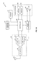
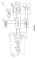
- Figs. 1A and 1B are block diagrams of an exemplary mobile communication device 10 according to the present invention.
- the exemplary embodiments comprise a cellular telephone; however, those skilled in the art will recognize that the present invention may be used in a variety of mobile communication devices 10 including personal digital assistants (PDA), palm computers, and other pervasive computing devices that communicate wirelessly.
- PDA personal digital assistants
- palm computers and other pervasive computing devices that communicate wirelessly.
- Mobile communication device 10 comprises controller 12, memory 14, audio processing circuit 16, position sensors 18, user interface 20, transceiver 30, and antenna 50.
- Controller 12 controls the operation of mobile communication device 10 according to programs stored in memory 14.
- the controller 12 may comprise, for example, one or more microprocessors, hardware, firmware, or a combination thereof. Suitable microprocessors may include, for example, both general purpose and special purpose microprocessors and digital signal processors.
- Memory 14 represents the entire hierarchy of memory in a mobile communication device 10, and may include both random access memory (RAM) and read-only memory (ROM).
- Computer program instructions and data required for operation are stored in nonvolatile memory, such as EPROM, EEPROM, and/or flash memory, which may be implemented as discrete devices, stacked devices, or integrated with controller 12.
- One or more position sensors 18 are used to detect the position of the user's hands and/or fingers when holding the mobile communication device 10. As will be described in more detail below, controller 12 uses the detected hand position to adjust the source impedance of the transmitter 32 based on the position of the user's hands.
- User interface 20 includes a keypad 22 and/or other input device, display 24, microphone 26, and speaker 28.
- Keypad 22 and display 24 enable the user to interact with the mobile communication device 10.
- Keypad 22 allows the user to dial numbers, enter commands, and navigate menus presented on display 24 to select desired options.
- Display 24 allows the user to see dialed numbers, status information, prompts, menus, and other information. Display 24 also allows the user to view and read messages and to view images and graphics.
- Microphone 26 converts the user's speech into electrical audio signals for transmission by the transceiver 30, and speaker 28 converts audio signals received by the transceiver 30 into audible signals that can be heard by the user.
- Audio processing circuit 16 provides basic analog output signals to speaker 28 and accepts analog audio input signals from microphone 26.
- Transceiver 30 is coupled to antenna 50 for receiving and transmitting signals.
- Transceiver 30 is a fully functional cellular radio transceiver, which may operate according to any known standard, including the standards known generally as the Global System for Mobile Communications (GSM), TIA/EIA-136, cdmaOne, cdma2000, UMTS, and Wideband CDMA.
- Transceiver 30 includes a transmitter 32 and a receiver 34 coupled to the antenna 50 through an RF switching circuit 36. Electrical signals from transmitter 32 are applied to antenna 50, which converts the electrical signals into electromagnetic waves that radiate out from the antenna 50. Conversely, when antenna 50 is subjected to electromagnetic waves radiating through space, the electromagnetic waves are converted by the antenna 50 into an electrical signal that is applied to the receiver 34.
- transmitter 32 and/or the receiver 34 include an adaptive impedance matching circuit 38 to match the source impedance of the transmitter 32 to the antenna impedance, as will be described in greater detail below.
- the adaptive matching may be positioned between the RF switch 36 and the antenna 50.
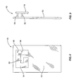
- Figs. 2 and 3 illustrate the physical appearance of a typical mobile communication device 10.
- the mobile communication device 10 includes a housing 40 having a front 42 and a back 44.
- the keypad 22, display 24, microphone 26 and speaker 28 are disposed on the front 42 of housing 40.
- a removable battery pack 46 is disposed on the back 44 of housing 40.
- the internal antenna 50 is located on the backside above the battery pack 46 to radiate electromagnetic energy away from the user.
- Internal antenna 50 may be a planar antenna, such as a microstrip antenna, patch antenna, monopole antenna, or inverted F antenna.
- Figs. 4 and 5 illustrate an exemplary planar inverted F antenna (PIFA) 50 for use with the present invention.
- a PIFA is generally a quarter wavelength resonant antenna achieved by short-circuiting the radiating element to the ground plane using a shorting conductor.
- the PIFA 50 shown in Figs. 4 and 5 includes a planar radiating element 54, an antenna feed 56, a conductive shorting member 58, and a ground plane 52 with air as a dielectric. In most mobile terminals, the printed circuit board functions as the ground plane 52.
- Antenna feed 56 is typically a metal strip or conductive member connecting the radiating element 54 to a fixed impedance feed line located on the PCB.
- the geometry of the feed structure plays an important role in tuning the impedance of the antenna 50.
- Conductive shorting member 58 conductively couples the radiating element 54 with the ground plane 52.
- PIFA 50 can be made to operate in multiple frequency bands by using a branched design or by adding grounded or floating parasitic elements.
- Fig. 4 shows a typical branched PIFA 50 with a single feed and an L-shaped slot 55, which is suitable for operation in the 800 MHz and 1900 Mhz or the 900 MHz and 1800 MHz bands.
- Fig. 6 illustrates a typical arrangement for placing PIFA 50 in a mobile communication device 10.
- a user will typically grasp the lower portions of housing 40 when using the mobile communication device 10. Consequently, internal antenna 50 is preferably placed adjacent an upper end of the backside 44 of housing 40 to avoid obstruction by the user's hand.
- the user's hand covers a relatively large portion of the housing 40, making it more difficult to avoid obstruction of the antenna 50.
- some of the energy radiated by internal antenna 50 is absorbed by human tissue, resulting in a loss of radiation efficiency.
- the presence of a human hand in close proximity to internal antenna 50 changes the impedance of internal antenna 50. If not corrected, the impedance mismatch results in further degradation of antenna performance, which can be substantial.
- the present invention compensates for changes in antenna impedance caused by the position of the user's hand on the back 44 of housing 40.
- position sensors 18 disposed on a back 44 of housing 40 of mobile communication device 10 detect the position of the user's hand, which for purposes of this application includes the user's fingers.
- Controller 12 uses the output signals from the sensor 18 to adjust the source impedance of the transmitter 32 and/or the receiver 34 based on the position of the user's hand. More particularly, the impedance matching circuit 38 varies the source impedance of the transmitter 32.
- the impedance matching circuit 38 comprises one or more reactive elements, such as shunt or series capacitors and/or inductors that can be reconfigured responsive to control signals from the controller 12 to vary the source impedance of the transmitter 32.
- the impedance matching circuit may contain multiple elements in T, ⁇ , or other configurations.
- the impedance matching circuit 38 includes one or more RF switches which may include MEMS, pin diodes, Gallium Arcsine switches (GAS) or other switches for switching the various capacitors and inductors into and out of the transmission path responsive to a control signal from controller 12.
- a variety of position sensors 18 may be used to detect the position of the user's hands, including capacitive sensors, light sensors, and resistive sensors.
- Preferred embodiments of the invention use film-type capacitive sensors that detect the variation in capacitance caused by the placement of the user's hands or fingers on the back 44 of housing 40.
- Film-type capacitive sensors can produce three-dimensional curved forms that conform to the housing geometry without losing its sensing function.
- One example of film-type capacitive sensors suitable for use with the present invention is marketed under the trade name GLIDEPOINT and is sold by ALPS Electric Company, Ltd. of Japan.
- Film-type capacitive sensors typically comprise two sets of orthogonal electrode arrays separated by a dielectric layer 106. The capacitively coupled electrode arrays form a grid with multiple sensing points that detect variations in capacitance caused by the proximity of the user's hand.
- Fig. 7 illustrates one possible arrangement of a film-type capacitive sensor 100 relative to the radiating element 54 of antenna 50.
- the capacitive sensor 100 extends along a side of the radiating element 54 adjacent the opening of the meandering slot 55, and may comprise a sensor with approximately 15 to 18 sensing points.
- the capacitive grid is disposed slightly below the antenna 50 to avoid capacitive coupling between sensor 100 and radiating element 54.
- capacitive sensor 100 detects when the user's hand or finger approaches the ends of the radiating element 54, which would have the effect of changing the antenna impedance by lengthening the antenna 50.
- capacitive sensor 100 may be placed on battery pack 46.
- the capacitive sensor 100 is disposed on the battery pack 46, it can be electrically coupled to PCB 52 by spring contacts or other flexible or rigid connectors in a conventional manner.
- battery pack 46 may be constructed to fit into a slot in the bottom or side of the housing 40. In this case, capacitive sensor 100 may be applied directly to the back 44 of housing 40.
- Fig. 8 shows an alternate embodiment of the invention using discrete resistive pressure sensors (or optical sensors) 110 as position sensors 18.
- the resistive pressure sensors 110 can be constructed using high resistivity materials that do not substantially interfere with the antenna 50 and therefore can be placed directly above the antenna 50. In the embodiment shown in Fig. 8 , the resistive pressure sensors 110 cover the area adjacent the ends of the radiating element 54, but could cover the entire area of the radiating element 54 if desired.
- Fig. 9 illustrates the operation of the controller 12.
- controller 12 obtains position information from the position sensor(s) 18 (block 202).
- the position sensor(s) 18 are powered only when mobile communication device 10 is transmitting or receiving to conserve battery power.
- controller 12 determines the state of each sensor or sensing point and adjusts the impedance of transmitter 32 based on the detected states (block 204, 206).
- the state of all of the sensors 18 or sensing points in a film type sensor corresponds to an n-bit codeword wherein each bit corresponds to one sensor or sensing position.
- a "0" at a given bit position in the codeword may, for example, indicate that the hand is not detected at the corresponding position on the housing 40, and a "1" at the given bit position may indicate that the hand is detected at the corresponding position on the housing 40.
- settings for the impedance matching circuit 38 correlated with each possible codeword are stored in a look-up table in memory 14.
- the settings stored in the look-up table may, for example, comprise an m-bit codeword representing a particular configuration for the impedance matching circuit 38.
- each bit in the m-bit codeword may correspond to a particular switch in the impedance matching circuit 38 and indicate the desired switch position.
- Fig. 10 illustrates an exemplary lookup table 150.
- the first column 152 of the lookup table 150 contains the all possible combinations of the sensor states, and the second column 154 contains corresponding settings.
- Controller 12 determines the appropriate settings for the impedance matching circuit 38 from the look-up table 150 and outputs one or more control signals to reconfigure the impedance matching circuit 38 (block 206).
- the mobile communication device 10 periodically determines the transmission/reception status (block 208) and repeats steps 202- 206 until mobile communication device 10 stops transmitting. The procedure terminates when mobile communication device 10 stops transmitting/receiving.
- the controller 12 may switch between multiple antenna feeds 56 and/or multiple shorting elements 58 to match the impedance of the antenna 50 with the transmitter and/or receiver.
- the impedance matching circuit 38 is placed between the RF switch 36 and the antenna 50 as shown in Fig. 1B .
- the impedance matching circuit comprises switching circuits 60 and 62 that select the ground element 58 and antenna feed 56 respectively.
- the impedance matching circuit 38 in this alternate embodiment may further include discrete components, such as shunt capacitors. In some embodiments, it may be possible to perform impedance matching without discrete components.
- the controller 12 selects an antenna feed configuration based on the position of the user's hand. Selection of the antenna feed configuration can be performed in the manner described above by using a lookup table correlating antenna feed configurations with sensor states.
Landscapes
- Engineering & Computer Science (AREA)
- Computer Networks & Wireless Communication (AREA)
- Signal Processing (AREA)
- Transceivers (AREA)
- Support Of Aerials (AREA)
- Input Circuits Of Receivers And Coupling Of Receivers And Audio Equipment (AREA)
Claims (17)
- Procédé d'ajustement de l'impédance source d'un émetteur (32) et/ou d'un récepteur (34) dans un dispositif de communication mobile (10) comportant un boîtier (40) et une antenne interne (50) placée de manière adjacente à une extrémité supérieure de la face arrière (44) du boîtier (40), comprenant le fait de:détecter une position d'une main d'un utilisateur sur le dispositif de communication mobile (10), en utilisant une pluralité de capteurs de position (18) disposés sur la face arrière (44) du boîtier (40), la pluralité de capteurs de position (18) formant un réseau de capteurs de position (18); etajuster de manière dynamique l'impédance source d'au moins l'un de l'émetteur (32) et du récepteur (34) dans le dispositif de communication mobile (10) sur la base de la position de la main de l'utilisateur,où la pluralité de capteurs de position (18) comportent au moins un capteur capacitif (100) qui est un capteur capacitif (100) de type film et qui forme une grille de capacités, disposé sous l'antenne interne (50).
- Procédé de la revendication 1, dans lequel l'ajustement dynamique de l'impédance source de l'émetteur (32) dans le dispositif de communication mobile (10) sur la base de la position de la main de l'utilisateur comprend le fait de déterminer une configuration de circuit pour un circuit (38) d'adaptation d'impédance sur la base de ladite position détectée de la main, et de générer un signal de commande pour reconfigurer le circuit (38) d'adaptation d'impédance sur la base de la configuration de circuit déterminée.
- Procédé de la revendication 2, comprenant en plus le fait de stocker des paramètres de configuration correspondant à une pluralité de configurations de circuit dans une table de conversion dans une mémoire (14).
- Procédé de la revendication 3, dans lequel le fait de déterminer une configuration de circuit pour un circuit (38) d'adaptation d'impédance sur la base de ladite position détectée de la main comprend l'utilisation de ladite position détectée de la main pour sélectionner une configuration de circuit.
- Circuit pour ajuster l'impédance source d'au moins l'un d'un émetteur (32) et d'un récepteur (34) dans un dispositif de communication mobile (10) comportant un boîtier (40) et une antenne interne (50) placée de manière adjacente à une extrémité supérieure de la face arrière (44) du boîtier (40), comprenant:une pluralité de capteurs de position (18), configurés de manière à être disposés sur la face arrière (44) du boîtier (40), pour détecter une position d'une main d'un utilisateur sur ledit dispositif de communication mobile (10), la pluralité de capteurs de position (18) formant un réseau de capteurs de position (18); etune unité de commande (12) pour ajuster de manière dynamique l'impédance source d'au moins l'un dudit émetteur (32) et dudit récepteur (34) sur la base de la position de la main de l'utilisateur,où la pluralité de capteurs de position (18) comportent au moins un capteur capacitif (100) qui est un capteur capacitif (100) du type film et qui forme une grille de capacités, disposé sous l'antenne interne (50).
- Circuit de la revendication 5, comprenant en plus un circuit (38) d'adaptation d'impédance couplant au moins l'un dudit émetteur (32) et dudit récepteur (34) à une antenne d'émission (50), ledit circuit (38) d'adaptation d'impédance ayant un ou plusieurs éléments réactifs qui peuvent être reconfigurés pour faire varier l'impédance source de l'émetteur (32) et/ou du récepteur (34).
- Circuit de la revendication 6, dans lequel un signal de commande délivré en sortie par ladite unité de commande (12) est agencé pour reconfigurer le circuit (38) d'adaptation d'impédance pour faire varier l'impédance source de l'émetteur (32) et/ou du récepteur (34).
- Circuit de la revendication 7, comprenant en plus une table de conversion stockée dans une mémoire (14) pour stocker une pluralité de configurations de circuit, où l'unité de commande (12) fonctionne pour sélectionner une configuration de circuit d'après ladite table de conversion sur la base de ladite position détectée de la main.
- Dispositif de communication mobile (10) comprenant:un boîtier (40);un émetteur (32) et un récepteur (34) dans ledit boîtier (40);une antenne interne (50) dans ledit boîtier (40) couplée audit émetteur (32) et audit récepteur (34), l'antenne interne (50) étant placée de manière adjacente à une extrémité supérieure de la face arrière (44) du boîtier (40); etun circuit selon l'une quelconque des revendication 5 à 8, avec sa pluralité de capteurs de position (18) disposés sur la face arrière (44) du boîtier (40) pour détecter une position d'une main d'un utilisateur sur ledit boîtier (40).
- Procédé d'ajustement de l'impédance d'une antenne d'un dispositif de communication mobile (10), comportant un boîtier (40) et une antenne interne (50) placée de manière adjacente à une extrémité supérieure de la face arrière (44) du boîtier (40), comprenant les étapes de:détecter une position d'une main d'un utilisateur sur le dispositif de communication mobile (10), en utilisant une pluralité de capteurs de position (18) disposés sur la face arrière du boîtier, la pluralité de capteurs de position (18) formant un réseau de capteurs de position (18); etajuster de manière dynamique l'impédance d'une antenne (50) pour le dispositif de communication mobile (10) en basculant de manière sélective entre plusieurs configurations de sources d'antenne,où la pluralité de capteurs de position (18) comportent au moins un capteur capacitif (100) qui est un capteur capacitif (100) du type film et qui forme une grille de capacités, disposé sous l'antenne interne (50).
- Procédé de la revendication 10, dans lequel le fait de basculer sélectivement entre plusieurs configurations de sources d'antenne comprend le fait de basculer de manière sélective entre plusieurs sources d'antenne (56) pour l'antenne (50).
- Procédé de la revendication 11, dans lequel le fait de basculer sélectivement entre plusieurs configurations de sources d'antenne comprend en plus le fait de basculer de manière sélective entre plusieurs éléments de court-circuitage (58) pour l'antenne (50).
- Procédé de la revendication 10, dans lequel le fait de basculer sélectivement entre plusieurs configurations de sources d'antenne comprend le fait de basculer de manière sélective entre plusieurs éléments de court-circuitage (58) pour l'antenne (50).
- Circuit pour ajuster l'impédance d'une antenne (50) dans un dispositif de communication mobile (10) comprenant un boîtier (40) et une antenne interne (50) placée de manière adjacente à une extrémité supérieure de la face arrière (44) du boîtier (40), comprenant:une pluralité de capteurs de position (18), configurés pour être disposés sur la face arrière (44) du boîtier, pour détecter une position d'une main d'un utilisateur sur ledit dispositif de communication mobile (10), la pluralité de capteurs de position (18) formant un réseau de capteurs de position (18);une unité de commande (12) pour ajuster de manière dynamique l'impédance de l'antenne (50) en basculant de manière sélective entre plusieurs configurations de sources d'antenne sur la base de la position de la main de l'utilisateuroù la pluralité de capteurs de position (18) comportent au moins un capteur capacitif (100) qui est un capteur capacitif (100) du type film et qui forme une grille de capacités, disposé sous l'antenne interne (50).
- Circuit de la revendication 14, dans lequel l'antenne a plusieurs sources (56) d'antenne (50) et dans lequel l'unité de commande (12) est configurée pour basculer entre plusieurs configurations d'antenne en sélectionnant l'une desdites sources d'antenne (56) multiples.
- Circuit de la revendication 14, dans lequel l'antenne (50) a plusieurs éléments de court-circuitage (58) et dans lequel l'unité de commande (12) est configurée pour basculer entre plusieurs configurations d'antenne en sélectionnant l'un desdits plusieurs éléments de court-circuitage (58).
- Dispositif de communication mobile (10) comprenant:un boîtier (40);un émetteur (32) et un récepteur (34) dans ledit boîtier (40);une antenne interne (50) dans ledit boîtier (40) couplée audit émetteur (32) et audit récepteur (34), ladite antenne (50) ayant une configuration de sources d'antenne variable et ladite antenne étant placée de manière adjacente à une extrémité supérieure de la face arrière (44) du boîtier (40);un circuit selon l'une quelconque des revendications 14 à 16, sa pluralité de capteurs de position (40) étant disposés sur la face arrière (44) du boîtier (40) pour détecter une position d'une main d'un utilisateur sur ledit boîtier (40).
Applications Claiming Priority (2)
| Application Number | Priority Date | Filing Date | Title |
|---|---|---|---|
| US10/837,829 US20050245204A1 (en) | 2004-05-03 | 2004-05-03 | Impedance matching circuit for a mobile communication device |
| PCT/US2004/038029 WO2005112280A1 (fr) | 2004-05-03 | 2004-11-12 | Circuit d'adaptation d'impedance pour dispositif de communication mobile |
Publications (2)
| Publication Number | Publication Date |
|---|---|
| EP1743432A1 EP1743432A1 (fr) | 2007-01-17 |
| EP1743432B1 true EP1743432B1 (fr) | 2009-03-18 |
Family
ID=34959526
Family Applications (1)
| Application Number | Title | Priority Date | Filing Date |
|---|---|---|---|
| EP04810967A Expired - Lifetime EP1743432B1 (fr) | 2004-05-03 | 2004-11-12 | Circuit d'adaptation d'impedance pour dispositif de communication mobile |
Country Status (6)
| Country | Link |
|---|---|
| US (2) | US20050245204A1 (fr) |
| EP (1) | EP1743432B1 (fr) |
| JP (1) | JP2007536797A (fr) |
| CN (1) | CN101015128A (fr) |
| DE (1) | DE602004020121D1 (fr) |
| WO (1) | WO2005112280A1 (fr) |
Families Citing this family (82)
| Publication number | Priority date | Publication date | Assignee | Title |
|---|---|---|---|---|
| JP4813489B2 (ja) * | 2004-09-09 | 2011-11-09 | エプコス アクチエンゲゼルシャフト | ビデオ受信機のアンテナ整合におけるまたは関する改良 |
| WO2007058910A2 (fr) * | 2005-11-10 | 2007-05-24 | Kathleen Lowe Melde | Appareil et procede de selection de composants pour circuit d'equilibre des impedances reconfigurable |
| US8162236B2 (en) | 2006-04-20 | 2012-04-24 | Masco Corporation Of Indiana | Electronic user interface for electronic mixing of water for residential faucets |
| US9243756B2 (en) | 2006-04-20 | 2016-01-26 | Delta Faucet Company | Capacitive user interface for a faucet and method of forming |
| KR100726260B1 (ko) * | 2006-08-07 | 2007-06-08 | 삼성전자주식회사 | 통신 장치의 정합 제어 장치 및 방법 |
| US20080076354A1 (en) * | 2006-09-26 | 2008-03-27 | Broadcom Corporation, A California Corporation | Cable modem with programmable antenna and methods for use therewith |
| US20080111748A1 (en) * | 2006-11-10 | 2008-05-15 | Dunn Doug L | Antenna system having plural selectable antenna feed points and method of operation thereof |
| CN101641869A (zh) * | 2007-01-31 | 2010-02-03 | 诺基亚公司 | 用于天线单元的阻抗和负载相位的补偿的设备 |
| US20090017910A1 (en) | 2007-06-22 | 2009-01-15 | Broadcom Corporation | Position and motion tracking of an object |
| US8892049B2 (en) * | 2007-10-10 | 2014-11-18 | Apple Inc. | Handheld electronic devices with antenna power monitoring |
| US9030361B2 (en) * | 2008-03-05 | 2015-05-12 | Ethertronics, Inc. | Automatic signal, SAR, and HAC adjustment with modal antenna using proximity sensors or pre-defined conditions |
| US8633863B2 (en) * | 2008-03-05 | 2014-01-21 | Ethertronics, Inc. | Modal adaptive antenna using pilot signal in CDMA mobile communication system and related signal receiving method |
| US9130407B2 (en) | 2008-05-13 | 2015-09-08 | Qualcomm Incorporated | Signaling charging in wireless power environment |
| EP2120287A1 (fr) | 2008-05-16 | 2009-11-18 | Laird Technologies AB | Dispositif d'antenne |
| US8417296B2 (en) * | 2008-06-05 | 2013-04-09 | Apple Inc. | Electronic device with proximity-based radio power control |
| AU2013205781B2 (en) * | 2008-11-06 | 2016-01-21 | Antenna79, Inc. | Radiation redirecting external case for portable communication device and antenna embedded in battery of portable communication device |
| US8214003B2 (en) | 2009-03-13 | 2012-07-03 | Pong Research Corporation | RF radiation redirection away from portable communication device user |
| US9172134B2 (en) | 2008-11-06 | 2015-10-27 | Antenna79, Inc. | Protective cover for a wireless device |
| US8957813B2 (en) | 2009-03-13 | 2015-02-17 | Pong Research Corporation | External case for redistribution of RF radiation away from wireless communication device user and wireless communication device incorporating RF radiation redistribution elements |
| WO2010054246A1 (fr) | 2008-11-06 | 2010-05-14 | Wong Alfred Y | Boîtier externe de redirection de rayonnement destiné à un dispositif de communication portatif et antenne intégrée à la batterie d’un dispositif de communication portatif |
| US8502618B2 (en) * | 2008-12-12 | 2013-08-06 | International Business Machines Corporation | Measurement and control of electromagnetic interference |
| US20100201312A1 (en) | 2009-02-10 | 2010-08-12 | Qualcomm Incorporated | Wireless power transfer for portable enclosures |
| US9166294B2 (en) | 2009-03-31 | 2015-10-20 | Tyco Safety Products Canada Ltd. | Quad-band PCB antenna |
| US8614650B2 (en) * | 2009-03-31 | 2013-12-24 | Tyco Safety Products Canada Ltd. | Tunable inverted F antenna |
| CN101945498B (zh) * | 2009-07-06 | 2014-10-29 | 宏达国际电子股份有限公司 | 通讯装置及信号处理方法 |
| US8466839B2 (en) * | 2009-07-17 | 2013-06-18 | Apple Inc. | Electronic devices with parasitic antenna resonating elements that reduce near field radiation |
| US8432322B2 (en) * | 2009-07-17 | 2013-04-30 | Apple Inc. | Electronic devices with capacitive proximity sensors for proximity-based radio-frequency power control |
| GB2472779B (en) * | 2009-08-17 | 2013-08-14 | Microsoft Corp | Antennas with multiple feed circuits |
| JP5370488B2 (ja) * | 2009-08-25 | 2013-12-18 | 株式会社村田製作所 | アンテナ装置 |
| FI20096101A0 (fi) * | 2009-10-27 | 2009-10-27 | Pulse Finland Oy | Menetelmä ja järjestely antennin sovittamiseksi |
| CN102170305A (zh) * | 2010-02-26 | 2011-08-31 | 深圳富泰宏精密工业有限公司 | 天线特性控制系统及方法 |
| US8781420B2 (en) | 2010-04-13 | 2014-07-15 | Apple Inc. | Adjustable wireless circuitry with antenna-based proximity detector |
| WO2011134534A1 (fr) | 2010-04-30 | 2011-11-03 | Epcos Ag | Module d'antenne adaptatif |
| US8406806B2 (en) * | 2010-09-20 | 2013-03-26 | Smartech Worldwide Limited | Mobile telephone capable of automatically switching antenna according to user's hand position |
| US8559869B2 (en) | 2011-09-21 | 2013-10-15 | Daniel R. Ash, JR. | Smart channel selective repeater |
| CN102437835B (zh) * | 2010-09-29 | 2016-09-28 | 宏达国际电子股份有限公司 | 移动通讯装置的阻抗匹配装置与方法 |
| CN102006028B (zh) * | 2010-11-15 | 2014-07-02 | 中兴通讯股份有限公司 | 一种阻抗匹配的方法及电路 |
| JP5534027B2 (ja) * | 2010-11-18 | 2014-06-25 | 株式会社村田製作所 | アンテナ装置 |
| US20120154070A1 (en) * | 2010-12-16 | 2012-06-21 | Sony Ericsson Mobile Communications Ab | Closed Loop Antenna Tuning Using Transmit Power Control Commands |
| US8577289B2 (en) | 2011-02-17 | 2013-11-05 | Apple Inc. | Antenna with integrated proximity sensor for proximity-based radio-frequency power control |
| US9074357B2 (en) | 2011-04-25 | 2015-07-07 | Delta Faucet Company | Mounting bracket for electronic kitchen faucet |
| TWI474631B (zh) * | 2011-07-27 | 2015-02-21 | Jieng Tai Internat Electric Corp | 無線通訊電路與無線通訊方法 |
| US9057184B2 (en) | 2011-10-19 | 2015-06-16 | Delta Faucet Company | Insulator base for electronic faucet |
| US9838060B2 (en) | 2011-11-02 | 2017-12-05 | Antenna79, Inc. | Protective cover for a wireless device |
| US9281849B2 (en) | 2012-03-26 | 2016-03-08 | Google Technology Holdings LLC | Method and apparatus for compensating for phase shift in a communication device |
| US9014245B2 (en) * | 2012-03-26 | 2015-04-21 | Google Technology Holdings LLC | Method and apparatus for compensating for phase shift in a communication device |
| US9048524B2 (en) | 2012-03-26 | 2015-06-02 | Google Technology Holdings LLC | Method and apparatus for compensating for phase shift in a communication device |
| US9201548B2 (en) * | 2012-05-03 | 2015-12-01 | Texas Instruments Incorporated | Material-discerning proximity sensing |
| US9154608B2 (en) * | 2012-05-09 | 2015-10-06 | Facebook, Inc. | Data exchange between antenna and modem of mobile device |
| US9093745B2 (en) | 2012-05-10 | 2015-07-28 | Apple Inc. | Antenna and proximity sensor structures having printed circuit and dielectric carrier layers |
| US9680218B2 (en) * | 2012-06-22 | 2017-06-13 | Blackberry Limited | Method and apparatus for controlling an antenna |
| US9363350B2 (en) * | 2012-07-05 | 2016-06-07 | Blackberry Limited | Methods and devices for detecting a hand |
| US20140015719A1 (en) * | 2012-07-13 | 2014-01-16 | Pulse Finland Oy | Switched antenna apparatus and methods |
| US9154189B2 (en) * | 2012-08-17 | 2015-10-06 | Qualcomm Incorporated | Wireless power system with capacitive proximity sensing |
| US9276312B2 (en) | 2013-03-13 | 2016-03-01 | Intel Deutschland Gmbh | Antenna tuner control system using state tables |
| US9333698B2 (en) | 2013-03-15 | 2016-05-10 | Delta Faucet Company | Faucet base ring |
| US9300342B2 (en) | 2013-04-18 | 2016-03-29 | Apple Inc. | Wireless device with dynamically adjusted maximum transmit powers |
| CN104348502B (zh) * | 2013-07-23 | 2017-02-08 | 维沃移动通信有限公司 | 一种移动终端的天线状态自适应方法及对应的移动终端 |
| US9059505B1 (en) * | 2013-12-31 | 2015-06-16 | Google Technology Holdings LLC | Systems and methods for a reconfigurable antenna using design elements on an electronic device housing |
| US9379445B2 (en) | 2014-02-14 | 2016-06-28 | Apple Inc. | Electronic device with satellite navigation system slot antennas |
| US9398456B2 (en) | 2014-03-07 | 2016-07-19 | Apple Inc. | Electronic device with accessory-based transmit power control |
| US9583838B2 (en) | 2014-03-20 | 2017-02-28 | Apple Inc. | Electronic device with indirectly fed slot antennas |
| US9559425B2 (en) | 2014-03-20 | 2017-01-31 | Apple Inc. | Electronic device with slot antenna and proximity sensor |
| US9728858B2 (en) | 2014-04-24 | 2017-08-08 | Apple Inc. | Electronic devices with hybrid antennas |
| US9791490B2 (en) | 2014-06-09 | 2017-10-17 | Apple Inc. | Electronic device having coupler for tapping antenna signals |
| US9444425B2 (en) | 2014-06-20 | 2016-09-13 | Apple Inc. | Electronic device with adjustable wireless circuitry |
| US9537219B2 (en) * | 2014-09-29 | 2017-01-03 | Apple Inc. | Electronic device with passive antenna retuning circuitry |
| CN105703846A (zh) * | 2014-11-28 | 2016-06-22 | 展讯通信(上海)有限公司 | 检测移动终端使用状态自适应调整天线状态的系统及方法 |
| US10128560B2 (en) | 2014-12-12 | 2018-11-13 | Ethertronics, Inc. | Hybrid antenna and integrated proximity sensor using a shared conductive structure |
| CN204376972U (zh) * | 2015-01-09 | 2015-06-03 | 中兴通讯股份有限公司 | 一种终端 |
| US10218052B2 (en) | 2015-05-12 | 2019-02-26 | Apple Inc. | Electronic device with tunable hybrid antennas |
| US9553640B1 (en) * | 2015-12-22 | 2017-01-24 | Microsoft Technology Licensing, Llc | Using multi-feed antennas |
| US10490881B2 (en) | 2016-03-10 | 2019-11-26 | Apple Inc. | Tuning circuits for hybrid electronic device antennas |
| TWI602406B (zh) * | 2016-07-20 | 2017-10-11 | 晶鈦國際電子股份有限公司 | 通訊裝置 |
| US10075570B2 (en) | 2016-08-09 | 2018-09-11 | Microsoft Technology Licensing, Llc | Providing sensing ability with a wireless communication apparatus |
| US10290946B2 (en) | 2016-09-23 | 2019-05-14 | Apple Inc. | Hybrid electronic device antennas having parasitic resonating elements |
| WO2018126247A2 (fr) | 2017-01-02 | 2018-07-05 | Mojoose, Inc. | Indicateur automatique d'intensité de signal et commutateur automatique d'antenne |
| US10393363B2 (en) | 2017-04-25 | 2019-08-27 | Delta Faucet Company | Illumination device for a fluid delivery apparatus |
| DE102019000919B4 (de) * | 2019-02-08 | 2025-07-10 | Diehl Ako Stiftung & Co. Kg | Berührungs- und/oder annäherungsempfindliche Eingabevorrichtung |
| US11576021B2 (en) * | 2020-03-23 | 2023-02-07 | Sap Se | Data processing system for detecting events and providing notifications |
| US20210313697A1 (en) * | 2020-04-02 | 2021-10-07 | Star Systems International Limited | Patch antenna |
| US12512583B2 (en) * | 2021-09-23 | 2025-12-30 | Semtech Corporation | Proximity sensor for RF control |
Citations (2)
| Publication number | Priority date | Publication date | Assignee | Title |
|---|---|---|---|---|
| US20020021278A1 (en) * | 2000-07-17 | 2002-02-21 | Hinckley Kenneth P. | Method and apparatus using multiple sensors in a device with a display |
| GB2387504A (en) * | 2002-04-12 | 2003-10-15 | Motorola Inc | Method of managing a user interface of a mobile communications device |
Family Cites Families (18)
| Publication number | Priority date | Publication date | Assignee | Title |
|---|---|---|---|---|
| US5673001A (en) * | 1995-06-07 | 1997-09-30 | Motorola, Inc. | Method and apparatus for amplifying a signal |
| JPH0964758A (ja) * | 1995-08-30 | 1997-03-07 | Matsushita Electric Ind Co Ltd | ディジタル携帯無線機の送信装置とそれに用いる高周波電力増幅装置 |
| US6356535B1 (en) * | 1998-02-04 | 2002-03-12 | Micron Technology, Inc. | Communication systems and methods of communicating |
| GB9806612D0 (en) * | 1998-03-28 | 1998-05-27 | Philips Electronics Nv | Communication device |
| JP2001217624A (ja) * | 2000-01-31 | 2001-08-10 | Denso Corp | 無線通信装置 |
| JP3618621B2 (ja) * | 2000-02-09 | 2005-02-09 | 株式会社ケンウッド | 移動通信端末 |
| JP2002185372A (ja) * | 2000-12-15 | 2002-06-28 | Matsushita Electric Ind Co Ltd | アンテナ切換機能を有する携帯無線装置 |
| JP2002217803A (ja) * | 2001-01-15 | 2002-08-02 | Nec Access Technica Ltd | 携帯無線端末装置 |
| US6862433B2 (en) * | 2001-02-06 | 2005-03-01 | Motorola, Inc. | Antenna system for a wireless information device |
| FI113813B (fi) * | 2001-04-02 | 2004-06-15 | Nokia Corp | Sähköisesti viritettävä monikaistainen tasoantenni |
| US7071776B2 (en) * | 2001-10-22 | 2006-07-04 | Kyocera Wireless Corp. | Systems and methods for controlling output power in a communication device |
| US6657595B1 (en) * | 2002-05-09 | 2003-12-02 | Motorola, Inc. | Sensor-driven adaptive counterpoise antenna system |
| JP3744883B2 (ja) * | 2002-06-05 | 2006-02-15 | 日本電気株式会社 | 携帯電話機、これに内蔵された解析装置、及びその解析方法 |
| FI114057B (fi) * | 2002-10-18 | 2004-07-30 | Nokia Corp | Menetelmä ja järjestely kuorman epäsovituksen havaitsemiseksi, sekä sellaista käyttävä radiolaite |
| US7072620B2 (en) * | 2003-04-03 | 2006-07-04 | Kyocera Wireless Corp. | System and method for regulating antenna electrical length |
| US6985113B2 (en) * | 2003-04-18 | 2006-01-10 | Matsushita Electric Industrial Co., Ltd. | Radio antenna apparatus provided with controller for controlling SAR and radio communication apparatus using the same radio antenna apparatus |
| JP3931163B2 (ja) * | 2003-08-14 | 2007-06-13 | 松下電器産業株式会社 | アンテナ整合装置 |
| US7236065B2 (en) * | 2004-04-28 | 2007-06-26 | Nokia Corporation | Integrated RF-front end having an adjustable antenna |
-
2004
- 2004-05-03 US US10/837,829 patent/US20050245204A1/en not_active Abandoned
- 2004-11-12 DE DE602004020121T patent/DE602004020121D1/de not_active Expired - Fee Related
- 2004-11-12 EP EP04810967A patent/EP1743432B1/fr not_active Expired - Lifetime
- 2004-11-12 CN CNA2004800434537A patent/CN101015128A/zh active Pending
- 2004-11-12 WO PCT/US2004/038029 patent/WO2005112280A1/fr not_active Ceased
- 2004-11-12 JP JP2007511350A patent/JP2007536797A/ja active Pending
-
2007
- 2007-06-21 US US11/766,323 patent/US20070241977A1/en not_active Abandoned
Patent Citations (2)
| Publication number | Priority date | Publication date | Assignee | Title |
|---|---|---|---|---|
| US20020021278A1 (en) * | 2000-07-17 | 2002-02-21 | Hinckley Kenneth P. | Method and apparatus using multiple sensors in a device with a display |
| GB2387504A (en) * | 2002-04-12 | 2003-10-15 | Motorola Inc | Method of managing a user interface of a mobile communications device |
Also Published As
| Publication number | Publication date |
|---|---|
| US20050245204A1 (en) | 2005-11-03 |
| EP1743432A1 (fr) | 2007-01-17 |
| JP2007536797A (ja) | 2007-12-13 |
| DE602004020121D1 (de) | 2009-04-30 |
| CN101015128A (zh) | 2007-08-08 |
| WO2005112280A1 (fr) | 2005-11-24 |
| US20070241977A1 (en) | 2007-10-18 |
Similar Documents
| Publication | Publication Date | Title |
|---|---|---|
| US20050245204A1 (en) | Impedance matching circuit for a mobile communication device | |
| US10069192B2 (en) | Portable communication device | |
| JP5770135B2 (ja) | 複数のアンテナモ−ドをサポ−トする動的に調整可能なアンテナ | |
| US6822611B1 (en) | Wideband internal antenna for communication device | |
| US6943733B2 (en) | Multi-band planar inverted-F antennas including floating parasitic elements and wireless terminals incorporating the same | |
| US7642966B2 (en) | Carrier and device | |
| US6348897B1 (en) | Multi-function antenna system for radio communication device | |
| KR101634274B1 (ko) | 안테나 구조체 | |
| US20050017909A1 (en) | External modular antennas and wireless terminals incorporating the same | |
| JP2007538459A (ja) | 別々の低周波数帯アンテナを複数含むマルチバンドアンテナシステムとそれを組み込んだ無線端末及び無線電話機 | |
| US20120319918A1 (en) | Antenna matching apparatus and methods | |
| EP1903633A1 (fr) | Antenne intégrée pour terminal portable | |
| EP2064774A1 (fr) | Antennes accordables pour dispositifs portables | |
| WO2002063713A2 (fr) | Antennes a fente et dispositifs de communications hertziennes les contenant | |
| WO2008010149A1 (fr) | Antenne à sensibilité réduite envers la position des doigts de l'utilisateur | |
| EP1686647B1 (fr) | Terminal de communication mobile | |
| US7439919B2 (en) | Multilayer PCB antenna | |
| US20070139271A1 (en) | Method for access to a medium by a multi-channel device | |
| FI124886B (fi) | PIFA-antenni, jossa on jatkettavissa oleva osa | |
| CN102349193A (zh) | 自适应天线阵列 | |
| JPH06112880A (ja) | 携帯無線機 | |
| KR20050081943A (ko) | 그라운드 판을 구비한 폴디드 모노폴 인테나 | |
| HK1179053B (en) | Dynamically adjustable antenna supporting multiple antenna modes |
Legal Events
| Date | Code | Title | Description |
|---|---|---|---|
| PUAI | Public reference made under article 153(3) epc to a published international application that has entered the european phase |
Free format text: ORIGINAL CODE: 0009012 |
|
| 17P | Request for examination filed |
Effective date: 20061031 |
|
| AK | Designated contracting states |
Kind code of ref document: A1 Designated state(s): DE GB GR |
|
| 17Q | First examination report despatched |
Effective date: 20070228 |
|
| RIN1 | Information on inventor provided before grant (corrected) |
Inventor name: VANCE, SCOTT, L. |
|
| DAX | Request for extension of the european patent (deleted) | ||
| RBV | Designated contracting states (corrected) |
Designated state(s): DE GB GR |
|
| GRAP | Despatch of communication of intention to grant a patent |
Free format text: ORIGINAL CODE: EPIDOSNIGR1 |
|
| RBV | Designated contracting states (corrected) |
Designated state(s): DE FR GB |
|
| GRAS | Grant fee paid |
Free format text: ORIGINAL CODE: EPIDOSNIGR3 |
|
| GRAA | (expected) grant |
Free format text: ORIGINAL CODE: 0009210 |
|
| AK | Designated contracting states |
Kind code of ref document: B1 Designated state(s): DE FR GB |
|
| REG | Reference to a national code |
Ref country code: GB Ref legal event code: FG4D |
|
| REF | Corresponds to: |
Ref document number: 602004020121 Country of ref document: DE Date of ref document: 20090430 Kind code of ref document: P |
|
| PLBE | No opposition filed within time limit |
Free format text: ORIGINAL CODE: 0009261 |
|
| STAA | Information on the status of an ep patent application or granted ep patent |
Free format text: STATUS: NO OPPOSITION FILED WITHIN TIME LIMIT |
|
| 26N | No opposition filed |
Effective date: 20091221 |
|
| GBPC | Gb: european patent ceased through non-payment of renewal fee |
Effective date: 20091112 |
|
| REG | Reference to a national code |
Ref country code: FR Ref legal event code: ST Effective date: 20100730 |
|
| PG25 | Lapsed in a contracting state [announced via postgrant information from national office to epo] |
Ref country code: FR Free format text: LAPSE BECAUSE OF NON-PAYMENT OF DUE FEES Effective date: 20091130 |
|
| PG25 | Lapsed in a contracting state [announced via postgrant information from national office to epo] |
Ref country code: DE Free format text: LAPSE BECAUSE OF NON-PAYMENT OF DUE FEES Effective date: 20100601 |
|
| PG25 | Lapsed in a contracting state [announced via postgrant information from national office to epo] |
Ref country code: GB Free format text: LAPSE BECAUSE OF NON-PAYMENT OF DUE FEES Effective date: 20091112 |