EP1743931A1 - Afficheur a cristaux liquide - Google Patents
Afficheur a cristaux liquide Download PDFInfo
- Publication number
- EP1743931A1 EP1743931A1 EP05720749A EP05720749A EP1743931A1 EP 1743931 A1 EP1743931 A1 EP 1743931A1 EP 05720749 A EP05720749 A EP 05720749A EP 05720749 A EP05720749 A EP 05720749A EP 1743931 A1 EP1743931 A1 EP 1743931A1
- Authority
- EP
- European Patent Office
- Prior art keywords
- liquid crystal
- polymer
- blue phase
- display device
- crystal display
- Prior art date
- Legal status (The legal status is an assumption and is not a legal conclusion. Google has not performed a legal analysis and makes no representation as to the accuracy of the status listed.)
- Granted
Links
Images


Classifications
-
- C—CHEMISTRY; METALLURGY
- C09—DYES; PAINTS; POLISHES; NATURAL RESINS; ADHESIVES; COMPOSITIONS NOT OTHERWISE PROVIDED FOR; APPLICATIONS OF MATERIALS NOT OTHERWISE PROVIDED FOR
- C09K—MATERIALS FOR MISCELLANEOUS APPLICATIONS, NOT PROVIDED FOR ELSEWHERE
- C09K19/00—Liquid crystal materials
- C09K19/52—Liquid crystal materials characterised by components which are not liquid crystals, e.g. additives with special physical aspect: solvents, solid particles
- C09K19/54—Additives having no specific mesophase characterised by their chemical composition
- C09K19/542—Macromolecular compounds
- C09K19/544—Macromolecular compounds as dispersing or encapsulating medium around the liquid crystal
-
- G—PHYSICS
- G02—OPTICS
- G02F—OPTICAL DEVICES OR ARRANGEMENTS FOR THE CONTROL OF LIGHT BY MODIFICATION OF THE OPTICAL PROPERTIES OF THE MEDIA OF THE ELEMENTS INVOLVED THEREIN; NON-LINEAR OPTICS; FREQUENCY-CHANGING OF LIGHT; OPTICAL LOGIC ELEMENTS; OPTICAL ANALOGUE/DIGITAL CONVERTERS
- G02F1/00—Devices or arrangements for the control of the intensity, colour, phase, polarisation or direction of light arriving from an independent light source, e.g. switching, gating or modulating; Non-linear optics
- G02F1/01—Devices or arrangements for the control of the intensity, colour, phase, polarisation or direction of light arriving from an independent light source, e.g. switching, gating or modulating; Non-linear optics for the control of the intensity, phase, polarisation or colour
- G02F1/13—Devices or arrangements for the control of the intensity, colour, phase, polarisation or direction of light arriving from an independent light source, e.g. switching, gating or modulating; Non-linear optics for the control of the intensity, phase, polarisation or colour based on liquid crystals, e.g. single liquid crystal display cells
- G02F1/137—Devices or arrangements for the control of the intensity, colour, phase, polarisation or direction of light arriving from an independent light source, e.g. switching, gating or modulating; Non-linear optics for the control of the intensity, phase, polarisation or colour based on liquid crystals, e.g. single liquid crystal display cells characterised by the electro-optical or magneto-optical effect, e.g. field-induced phase transition, orientation effect, guest-host interaction or dynamic scattering
-
- C—CHEMISTRY; METALLURGY
- C09—DYES; PAINTS; POLISHES; NATURAL RESINS; ADHESIVES; COMPOSITIONS NOT OTHERWISE PROVIDED FOR; APPLICATIONS OF MATERIALS NOT OTHERWISE PROVIDED FOR
- C09K—MATERIALS FOR MISCELLANEOUS APPLICATIONS, NOT PROVIDED FOR ELSEWHERE
- C09K19/00—Liquid crystal materials
- C09K19/02—Liquid crystal materials characterised by optical, electrical or physical properties of the components, in general
- C09K19/0275—Blue phase
-
- C—CHEMISTRY; METALLURGY
- C09—DYES; PAINTS; POLISHES; NATURAL RESINS; ADHESIVES; COMPOSITIONS NOT OTHERWISE PROVIDED FOR; APPLICATIONS OF MATERIALS NOT OTHERWISE PROVIDED FOR
- C09K—MATERIALS FOR MISCELLANEOUS APPLICATIONS, NOT PROVIDED FOR ELSEWHERE
- C09K19/00—Liquid crystal materials
- C09K19/52—Liquid crystal materials characterised by components which are not liquid crystals, e.g. additives with special physical aspect: solvents, solid particles
- C09K19/58—Dopants or charge transfer agents
- C09K19/586—Optically active dopants; chiral dopants
-
- G—PHYSICS
- G02—OPTICS
- G02F—OPTICAL DEVICES OR ARRANGEMENTS FOR THE CONTROL OF LIGHT BY MODIFICATION OF THE OPTICAL PROPERTIES OF THE MEDIA OF THE ELEMENTS INVOLVED THEREIN; NON-LINEAR OPTICS; FREQUENCY-CHANGING OF LIGHT; OPTICAL LOGIC ELEMENTS; OPTICAL ANALOGUE/DIGITAL CONVERTERS
- G02F1/00—Devices or arrangements for the control of the intensity, colour, phase, polarisation or direction of light arriving from an independent light source, e.g. switching, gating or modulating; Non-linear optics
- G02F1/01—Devices or arrangements for the control of the intensity, colour, phase, polarisation or direction of light arriving from an independent light source, e.g. switching, gating or modulating; Non-linear optics for the control of the intensity, phase, polarisation or colour
- G02F1/13—Devices or arrangements for the control of the intensity, colour, phase, polarisation or direction of light arriving from an independent light source, e.g. switching, gating or modulating; Non-linear optics for the control of the intensity, phase, polarisation or colour based on liquid crystals, e.g. single liquid crystal display cells
- G02F1/137—Devices or arrangements for the control of the intensity, colour, phase, polarisation or direction of light arriving from an independent light source, e.g. switching, gating or modulating; Non-linear optics for the control of the intensity, phase, polarisation or colour based on liquid crystals, e.g. single liquid crystal display cells characterised by the electro-optical or magneto-optical effect, e.g. field-induced phase transition, orientation effect, guest-host interaction or dynamic scattering
- G02F1/13718—Devices or arrangements for the control of the intensity, colour, phase, polarisation or direction of light arriving from an independent light source, e.g. switching, gating or modulating; Non-linear optics for the control of the intensity, phase, polarisation or colour based on liquid crystals, e.g. single liquid crystal display cells characterised by the electro-optical or magneto-optical effect, e.g. field-induced phase transition, orientation effect, guest-host interaction or dynamic scattering based on a change of the texture state of a cholesteric liquid crystal
-
- C—CHEMISTRY; METALLURGY
- C09—DYES; PAINTS; POLISHES; NATURAL RESINS; ADHESIVES; COMPOSITIONS NOT OTHERWISE PROVIDED FOR; APPLICATIONS OF MATERIALS NOT OTHERWISE PROVIDED FOR
- C09K—MATERIALS FOR MISCELLANEOUS APPLICATIONS, NOT PROVIDED FOR ELSEWHERE
- C09K19/00—Liquid crystal materials
- C09K19/52—Liquid crystal materials characterised by components which are not liquid crystals, e.g. additives with special physical aspect: solvents, solid particles
- C09K19/54—Additives having no specific mesophase characterised by their chemical composition
- C09K19/542—Macromolecular compounds
- C09K2019/546—Macromolecular compounds creating a polymeric network
-
- G—PHYSICS
- G02—OPTICS
- G02F—OPTICAL DEVICES OR ARRANGEMENTS FOR THE CONTROL OF LIGHT BY MODIFICATION OF THE OPTICAL PROPERTIES OF THE MEDIA OF THE ELEMENTS INVOLVED THEREIN; NON-LINEAR OPTICS; FREQUENCY-CHANGING OF LIGHT; OPTICAL LOGIC ELEMENTS; OPTICAL ANALOGUE/DIGITAL CONVERTERS
- G02F1/00—Devices or arrangements for the control of the intensity, colour, phase, polarisation or direction of light arriving from an independent light source, e.g. switching, gating or modulating; Non-linear optics
- G02F1/01—Devices or arrangements for the control of the intensity, colour, phase, polarisation or direction of light arriving from an independent light source, e.g. switching, gating or modulating; Non-linear optics for the control of the intensity, phase, polarisation or colour
- G02F1/13—Devices or arrangements for the control of the intensity, colour, phase, polarisation or direction of light arriving from an independent light source, e.g. switching, gating or modulating; Non-linear optics for the control of the intensity, phase, polarisation or colour based on liquid crystals, e.g. single liquid crystal display cells
- G02F1/133—Constructional arrangements; Operation of liquid crystal cells; Circuit arrangements
- G02F1/1333—Constructional arrangements; Manufacturing methods
- G02F1/1343—Electrodes
- G02F1/134309—Electrodes characterised by their geometrical arrangement
- G02F1/134363—Electrodes characterised by their geometrical arrangement for applying an electric field parallel to the substrate, i.e. in-plane switching [IPS]
-
- G—PHYSICS
- G02—OPTICS
- G02F—OPTICAL DEVICES OR ARRANGEMENTS FOR THE CONTROL OF LIGHT BY MODIFICATION OF THE OPTICAL PROPERTIES OF THE MEDIA OF THE ELEMENTS INVOLVED THEREIN; NON-LINEAR OPTICS; FREQUENCY-CHANGING OF LIGHT; OPTICAL LOGIC ELEMENTS; OPTICAL ANALOGUE/DIGITAL CONVERTERS
- G02F1/00—Devices or arrangements for the control of the intensity, colour, phase, polarisation or direction of light arriving from an independent light source, e.g. switching, gating or modulating; Non-linear optics
- G02F1/01—Devices or arrangements for the control of the intensity, colour, phase, polarisation or direction of light arriving from an independent light source, e.g. switching, gating or modulating; Non-linear optics for the control of the intensity, phase, polarisation or colour
- G02F1/13—Devices or arrangements for the control of the intensity, colour, phase, polarisation or direction of light arriving from an independent light source, e.g. switching, gating or modulating; Non-linear optics for the control of the intensity, phase, polarisation or colour based on liquid crystals, e.g. single liquid crystal display cells
- G02F1/137—Devices or arrangements for the control of the intensity, colour, phase, polarisation or direction of light arriving from an independent light source, e.g. switching, gating or modulating; Non-linear optics for the control of the intensity, phase, polarisation or colour based on liquid crystals, e.g. single liquid crystal display cells characterised by the electro-optical or magneto-optical effect, e.g. field-induced phase transition, orientation effect, guest-host interaction or dynamic scattering
- G02F1/13775—Polymer-stabilized liquid crystal layers
-
- G—PHYSICS
- G02—OPTICS
- G02F—OPTICAL DEVICES OR ARRANGEMENTS FOR THE CONTROL OF LIGHT BY MODIFICATION OF THE OPTICAL PROPERTIES OF THE MEDIA OF THE ELEMENTS INVOLVED THEREIN; NON-LINEAR OPTICS; FREQUENCY-CHANGING OF LIGHT; OPTICAL LOGIC ELEMENTS; OPTICAL ANALOGUE/DIGITAL CONVERTERS
- G02F1/00—Devices or arrangements for the control of the intensity, colour, phase, polarisation or direction of light arriving from an independent light source, e.g. switching, gating or modulating; Non-linear optics
- G02F1/01—Devices or arrangements for the control of the intensity, colour, phase, polarisation or direction of light arriving from an independent light source, e.g. switching, gating or modulating; Non-linear optics for the control of the intensity, phase, polarisation or colour
- G02F1/13—Devices or arrangements for the control of the intensity, colour, phase, polarisation or direction of light arriving from an independent light source, e.g. switching, gating or modulating; Non-linear optics for the control of the intensity, phase, polarisation or colour based on liquid crystals, e.g. single liquid crystal display cells
- G02F1/137—Devices or arrangements for the control of the intensity, colour, phase, polarisation or direction of light arriving from an independent light source, e.g. switching, gating or modulating; Non-linear optics for the control of the intensity, phase, polarisation or colour based on liquid crystals, e.g. single liquid crystal display cells characterised by the electro-optical or magneto-optical effect, e.g. field-induced phase transition, orientation effect, guest-host interaction or dynamic scattering
- G02F1/13793—Blue phases
Definitions
- the present invention relates to a liquid crystal display device using polymer-stabilized blue phase liquid crystals in an in-plane switching (IPS) mode.
- IPS in-plane switching
- Liquid crystal display devices are widely used in the optical data processing field.
- the conventional liquid display modes include TN, STN, IPS, VA (MVA), OCB and the like. All of these modes cause the liquid crystal molecular orientation already under control to change into a different state of orientation when electrical fields are applied and change the polarization direction and polarization state of the transmitted light. The changes are converted into light and dark contrasts in polarized boards and the like to generally form a display.
- These conventional liquid crystal display modes all require a surface orientation treatment in order to control the liquid crystal molecular orientation. A rubbing treatment is needed with the particular exception of VA (MVA).
- the rubbing treatment is an operation in which a cloth or the like is used to rub an orientation membrane that has been surface coated onto a substrate surface and is in contact with liquid crystals, and is the cause of increased costs associated with declining yields and poorer display qualities.
- all of the modes described above use nematic liquid crystals, and their response times are about ten milliseconds at the shortest, thus limiting their application in dynamic picture displays used for television.
- Chiral nematic liquid crystals were recently developed as liquid crystals for use in liquid crystal display devices (References 1 and 2).
- the inventors developed a polymer-stabilized blue phase liquid crystal to be used in place of the conventional nematic liquid crystals in order to solve the problems described above (Reference 3).
- These polymer-stabilized blue phase liquid crystals are novel materials having a tremendously expanded operational temperature range without losing the high speed responsiveness inherent in the blue phase.
- a polymer-stabilized blue phase is optically isotropic when no electrical field is applied, and the orientation does not need to be controlled.
- a display is realized using a novel mode involving no double refraction in the absence of an electrical field and a phenomenon that induces double refraction under applied electrical fields.
- the response time is about one hundred microseconds and is much faster than that of conventional liquid crystal display devices.
- an in-place switching (IPS) mode was developed in response to the demand for larger liquid crystal screens and better quality displays (References 4 and 5).
- An electrical field is applied on an equilibrium surface in a substrate in this mode, and a liquid crystal material compatible with this mode is being sought.
- the present invention is a liquid crystal display device that deals with an in-place switching (IPS) mode and presents a liquid crystal display device that does not require a surface orientation treatment and can dramatically improve the response rate that, in conventional liquid crystal displays, is inadequate for use in dynamic picture displays.
- IPS in-place switching
- BP polymer-stabilized blue phase liquid crystal
- the selective reflection in the visible light wavelength zone caused by the BP structure is the reason for light leakage when the display is black. Therefore, the present invention provides a liquid crystal display device that has no light leakage from a black screen, which means to yield a dark screen.
- the inventors discovered that a liquid crystal display device using polymer-stabilized blue phase liquid crystals (Reference 2) displayed a sizeable double refraction change when an electrical field was applied in the direction in-plane to a cell substrate and has a high potential to be used as display devices. Furthermore, the inventors discovered that a liquid crystal display device with no light leakage in a black display could be obtained by optimizing the type and amount of the chiral dopant added to the liquid crystals. The present invention was completed based on the discoveries.
- the liquid crystal display device of the present invention is suitable for creating larger and better quality liquid crystal screens used in an in-place switching (IPS) mode.
- IPS in-place switching
- no surface orientation treatment used for orientation control is necessary since polymer-stabilized blue phase liquid crystals are used. Therefore, the orientation treatment-washing-drying process such as coating-drying-heat curing-rubbing and the like of an oriented film on a substrate surface that used to be essential in conventional display devices can be completely eliminated.
- foreign material contamination caused by dust, fine particles and the like associated with the process described above, static electricity generation and declines in yield and quality caused by scratching can be avoided by this process.
- the response time of the conventional liquid crystal display devices was basically limited since the basic theory focused on the changes in the orientation state of nematic liquid crystals, and the dynamic picture display function of such elements was worse than that of plasma panels and EL, the competing technologies.
- a polymer-stabilized blue phase solved this problem since a response time in the order of about one hundred microseconds was possible.
- the diffraction wavelength of the liquid crystals can be controlled to the zone outside the visible light zone (from 380 nm to 750 nm).
- the liquid crystal display devices using such polymer-stabilized blue phase liquid crystals can avoid light leakage during black displays, which means to yield a dark visual field.
- the present invention is a liquid crystal display device comprising a polymer-stabilized blue phase liquid crystal sandwiched between a pair of clear substrates, wherein the polymer-stabilized blue phase liquid crystal comprises a low molecular weight liquid crystal that allows a blue phase to appear between a cholesteric phase and an isotropic phase and a polymer network formed in the low molecular weight liquid crystal, and an electrical field is applied parallel to the substrates.
- This electrical field is preferably applied using two toothed comb shaped electrodes incorporated alternately in one of the clear substrate surfaces.
- one of the two electrodes is used as the source electrode for a thin film transistor (TFT) and the other is used as the common electrode.
- TFT thin film transistor
- the TFT can act to turn the electrical field on and off.
- the polymer-stabilized blue phase liquid crystal contains a chiral dopant in this liquid crystal display device.
- the amount of chiral dopant in the polymer-stabilized blue phase liquid crystal is preferably adjusted so that the diffraction wavelength of the polymer-stabilized blue phase liquid crystal is outside the visible zone (from 380 nm to 750 nm).
- the present invention is a polymer-stabilized blue phase liquid crystal, which is constructed from a blue phase of a composite liquid crystal composition comprising a low molecular weight liquid crystal and a polymer network, wherein the low molecular weight liquid crystal allows a blue phase to appear between a cholesteric phase and an isotropic phase and a polymer network is formed by polymerizing non-liquid crystalline monomers along with a crosslinking agent, wherein the polymer-stabilized blue phase liquid crystal contains a chiral dopant and the amount of the chiral dopant per the amount of the polymer-stabilized blue phase liquid crystal is adjusted so that the diffraction wavelength of the polymer-stabihzed blue phase liquid crystal is outside visible zone (from 380 nm to 750 nm).
- the optical modulation element of the present invention comprises polymer-stabilized blue phase liquid crystals sandwiched between a pair of clear substrates. Glass, plastic films, optical crystals and the like may be used as clear substrates. The distance between a pair of these substrates is ordinarily from 2 ⁇ m to 100 ⁇ m.
- the electrical field applied is ordinarily from 1,000 V/cm to 100,000 V/cm. The electrical field may be basically parallel to the substrates (or perpendicular to the display direction).
- the method used to apply the electrical field is not particularly restricted, but a structure that incorporates two toothed, comb-shaped type electrodes alternately into one of the substrate surfaces is convenient.
- the preferred number of teeth per this toothed, comb-shaped electrode is from about two to one hundred, the preferred length is from about 1 ⁇ m to 10,000 ⁇ m, the preferred width is from about 1 ⁇ m to 50 ⁇ m and the preferred distance between comb teeth is from about 1 ⁇ m to 100 ⁇ m.
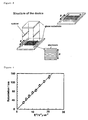
- FIG. 3 One example of the structure of the optical modulator device of the present invention is shown in Figure 3.
- two toothed, comb-shaped electrodes are incorporated alternately in a single plane of a substrate, and an electrical field is applied perpendicularly to the comb teeth or parallel to the substrate surface upon applying a voltage.
- the other substrate forming the sandwich using a spacer such as a thin film and the like is a glass sheet containing no electrodes.
- a gap with the thickness of the spacer used is formed between substrates, and a liquid crystal material is injected into the gap.
- a monoaxial refractive index anisotropy is generated with the optical axis in the direction of the electrical field, that is, in the direction perpendicular to the line of the toothed, comb-shaped electrodes.
- a cell is first positioned between two polarizing sheets, and the polarization light axis of the individual polarizing light sheets is intersected (in a so-called cross Nicol state).
- the transmittance ratio is zero (the double refraction becomes zero) at zero electrical field, and light transmission occurs as the electrical field is applied (the cell where double refraction occurred acts like a wavelength board). Therefore, a light-dark contrast can be created when the voltage is turned ON and OFF.
- the polymer-stabilized blue phase liquid crystal of the present invention comprises a low molecular weight liquid crystal and a polymer network.
- the monomer used to form the polymer network may be either a non-liquid crystalline monomer or a liquid crystalline monomer.
- a non-liquid crystalline monomer is more effective than a liquid crystalline monomer.
- the non-liquid crystalline monomer is a monomer that can undergo polymerization through photo polymerization or thermal polymerization and indicates a monomer that does not have a rod shaped molecular structure (for example, molecular structures with alkyl groups, cyano groups, fluorine and the like attached to termini such as biphenyl groups or biphenyl-cyclohexyl groups and the like).
- monomers containing polymerizable groups such as acryloyl groups, methacryloyl groups, vinyl groups, epoxy groups, fumarate groups, cinnamoyl groups and the like may be cited.
- non-liquid crystalline monomer is not restricted to these examples.
- liquid crystalline monomers containing phenyl groups, cyclohexyl groups and the like and having rod shaped or sheet shaped skeletons exhibiting liquid crystallinity themselves or upon mixing with other molecules may be cited.
- monomers containing multiple numbers of polymerization groups may also be used.
- acrylate type monomers containing acryloyl groups or methacryloyl groups in the molecular structure may be cited.
- Acrylate type monomers containing branched structure containing alkyl groups as side chains are particularly preferred.
- the alkyl groups are commonly alkyl groups containing from one to four carbon atoms, and monomers containing at least one side chain comprising such alkyl groups per monomer unit are used.
- cyclohexyl acrylate and the like may be cited.
- 2-ethylhexyl acrylate, 3, 3-trimethylhexyl acrylate and the like may be cited.
- a polymer network is formed upon subjecting this monomer to polymerization along with a crosslinking agent.
- This crosslinking agent may be either a liquid crystalline or non-liquid crystalline compound, and those containing a reactive segment that can form and yield a network structure by linking between monomer molecules corresponding to the monomer used should be used.
- a liquid crystalline diacrylate monomer may be used as a crosslinking agent when an acrylate type monomer is used as the monomer according to the preferred embodiment of the present invention.
- the low molecular weight liquid crystal is able to allow a blue phase to appear between a cholesteric phase (a chiral nematic phase) and an isotropic phase.
- Thermotropic liquid crystals comprising thin, rod shaped, geometrically shaped molecules are preferred, but various liquid crystal materials developed for use in liquid crystal display devices may also be used.
- This type of low molecular weight liquid crystals contains molecular structures such as biphenyl, terphenyl, biphenyl-cyclohexyl and the like.
- cholesteric phase chiral nematic phase
- chiral dopant a substance that may themselves exhibit chirality in the presence of asymmetric atoms or substances able to allow a cholesteric phase (chiral nematic phase) to appear upon adding a chiral like substance (chiral dopant).
- the substance is selected from those having a spiral pitch length in the cholesteric phase (chiral nematic phase) of about 500 nm or less.
- These low molecular weight liquid crystals are generally preferably used as mixtures of multiple numbers of them.
- a chiral dopant is a material that creates twisting structures in a liquid crystal.
- ZLI-4527 and CB15 Figure 1 used in the examples and the derivatives containing a furo[3,2-b] furan structure (see Figures 2a through h) and the like may be cited.
- a chiral dopant is ordinarily added as an additive to stabilize the twisting structures in a TN mode and to induce a helical phase such as cholesteric phases, chiral smectic phases and the like.
- a pitch length that is shorter than usual is preferred. Therefore, a chiral dopant with a large HTP and that is very soluble in the liquid crystal is preferred.
- the blue phase of the polymer-stabilized blue phase liquid crystal is obtained by dispersing a monomer and a crosslinking agent in a low molecular weight liquid phase and allowing a polymerization reaction to occur at a temperature that maintains the blue phase.
- the polymerization can be allowed to occur using either thermal polymerization or photo polymerization.
- thermal polymerization the temperature is limited to the temperature range in which a blue phase is maintained and the polymerization temperature (heating temperature) overlaps.
- photo polymerization using ultraviolet light is preferred since a potential for a polymer network to undergo changes upon heating exists.
- a polymerization initiator in addition to a monomer, a chiral dopant and a crosslinking agent is preferably dispersed in a low molecular weight liquid crystal for the polymerization in order to hasten the polymerization rate.
- various initiators such as acetophenone type, benzophenone type, benzoin ether type, thioxanthone type initiators and the like may be used. More specifically, 2,2-dimethoxy-2-phenyl acetophenone and the like may be listed as examples.
- the following procedure may be conducted to adjust the amount of a chiral dopant used per the amount of polymer-stabilized blue phase liquid crystals in order to adjust the diffraction wavelength of the polymer-stabilized blue phase liquid crystals in a range outside the visible zone (from 380 nm to 750 nm).
- DMPAP 2,2-dimethoxyphenylacetophenone
- a sandwich type glass cell was prepared using a glass substrate (E.H.C. Co., Ltd.) 1.1 mm thick with a toothed, comb-shaped type ITO electrode (ITO electrode resistance value: 100 ⁇ ) with the distance between electrodes of 50 ⁇ m on a substrate surface and a glass substrate 1.1 mm thick with no electrodes.
- the cell thickness was set at 25 ⁇ m using a spacer.
- the mixed solution described above in an isotropic phase was poured into the glass cell using a capillary phenomenon.
- the liquid phase that appeared using the mixed solution prepared was, from the high temperature side, BPII, BPI and chiral nematic phase.
- the glass cell temperature was maintained at a constant level in the temperature zone in which the composite system displayed BPI.
- a polymer-stabilized blue phase was prepared.
- the ultraviolet light irradiation procedure involved 1 s/five times, 2 s/twice, 3s .5s 15s ⁇ 30s ⁇ 30 min/once, and the irradiation spacing was 10s.
- the liquid crystal phase was identified using a polarized light microscope.
- the polarized light microscope used was an ECLIPSE E600W (Nikon Co., Ltd.), and the observation was conducted under a crossed Nicol state.
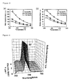
- the coordinate shows the degree of 632 nm light transmittance in the direction perpendicular to the substrate face at 293K.
- the magnitude of optical retardation induced by the electrical field increased in proportion to the square of the electrical field as did the Kerr effect.
- the Kerr coefficient was calculated from the slope in Figure 4 and was 3.7 x 10 -10 V -2 m and was about 180 times the Kerr coefficient of nitrobenzene. For an optically isotropic material, this was an unusually high value.
- the light transmittance reached a maximum when the optical retardation was one half of the wavelength of the light.
- a high voltage was ordinarily needed to make the optical retardation one half the wavelength of the transmitted light in this type of system.
- this type of condition was easily achieved when a liquid crystal with a high refractive index and a large induced anisotropy such as the polymer-stabilized blue phase liquid crystal in a liquid crystal display device of the present invention was used.
- This attenuation time was comparable to that of a low molecular weight blue phase at 325.5°K.
- the attenuation time in the high temperature zone was about 10 -6 s.
- This type of response time is extremely high [fast, short?] when compared to the response times of conventional liquid crystal display devices.
- a reflection spectrum in the presence of an electrical field for a polymer-stabilized BP prepared using a photo polymerizable monomer fraction ( ⁇ ) of 6.5 mole % is shown in Figure 6.
- the measurement was conducted at 298°K.
- the (110) diffraction peak of a BP grate observed in the vicinity of 489 nm was remarkable even after an electrical field was applied.
- the temperature dependence of the reflection spectrum for a (photo polymerizable monomer/liquid crystal) composite system is shown in Figure 7.
- the scanned wavelength zone was from 700 nm to 375 nm.
- the reflection spectrum clearly indicated that the BP appearance temperature range for the composite system was about 2.5°K.
- the inserted figures in Figure 7 were polarized light microscope images at the temperatures at which (a) blue phase (BP) and (b) chiral nematic phase or cholesteric phase (N*) appeared in the composite system.
- the diffraction wavelength of the BP appeared was 380 nm or lower, and the (a) was a dark field even in the area where BP appeared in the polarized light microscope images.
- a (b) focal-conic structure associated with N* was observed in a low temperature zone.
- BP polymer-stabilized.
- BP was prepared using photo polymerization.
- the optical structure of the BP that appeared could not be confirmed using a polarized microscope examination. Therefore, ultraviolet light irradiation was conducted from the BP/N* phase transition temperature observed to 2°K on the high temperature side.
- the irradiation mode used was the same as that described in Example 1.
- the temperature dependence of the reflection spectrum of the (polymer network/liquid crystal) composite system prepared was shown in Figure 8.
- a remarkable reflection peak indicating the appearance of BP was observed over a broad temperature range.
- the diffraction wavelength observed was in the vicinity of 370 nm.
- Figure 6 diffraction wavelength 480 nm
- the optimization of a chiral dopant was able to shift the diffraction wavelength to the ultraviolet region.
- the polarized light microscope image at 296.5°K was a dark field.
- the polarized light microscope images of the polymer-stabilized BP prepared before and after an electrical field was applied are shown in Figure 9. The observation was made at 293°K.
- the applied electrical field was a 4.9 V ⁇ m -1 sinusoidal wave alternating current electrical field at a frequency of 100 kHz.
- no electrical field was applied (a)
- the state of polarization of the incident light did not change upon passing through an optically isotropic polymer-stabilized BP
- the polarized light microscope image was a dark field.
- an electrical field was applied (b)
- a dramatic increase in the amount of transmitted light was observed indicating that a double refraction was induced in the polymer-stabilized BP between electrodes.
- the retardation measured using a monochromatic light source is plotted against the square of the applied electrical field in Figure 10.
- the measurements were conducted at 293°K.
- the Kerr coefficient was calculated and was found to be 2.05 x 10 -10 mV -2 . This value corresponded to a sixty fold increase over that of nitrobenzene.
Landscapes
- Chemical & Material Sciences (AREA)
- Crystallography & Structural Chemistry (AREA)
- Physics & Mathematics (AREA)
- Engineering & Computer Science (AREA)
- Materials Engineering (AREA)
- Organic Chemistry (AREA)
- Nonlinear Science (AREA)
- General Physics & Mathematics (AREA)
- Optics & Photonics (AREA)
- Liquid Crystal (AREA)
- Liquid Crystal Substances (AREA)
Applications Claiming Priority (3)
| Application Number | Priority Date | Filing Date | Title |
|---|---|---|---|
| JP2004079563 | 2004-03-19 | ||
| JP2004192448 | 2004-06-30 | ||
| PCT/JP2005/004481 WO2005090520A1 (fr) | 2004-03-19 | 2005-03-15 | Afficheur a cristaux liquide |
Publications (3)
| Publication Number | Publication Date |
|---|---|
| EP1743931A1 true EP1743931A1 (fr) | 2007-01-17 |
| EP1743931A4 EP1743931A4 (fr) | 2009-01-21 |
| EP1743931B1 EP1743931B1 (fr) | 2011-08-24 |
Family
ID=34993686
Family Applications (1)
| Application Number | Title | Priority Date | Filing Date |
|---|---|---|---|
| EP05720749A Expired - Lifetime EP1743931B1 (fr) | 2004-03-19 | 2005-03-15 | Afficheur a cristaux liquide |
Country Status (7)
| Country | Link |
|---|---|
| US (1) | US7576829B2 (fr) |
| EP (1) | EP1743931B1 (fr) |
| JP (1) | JP4766694B2 (fr) |
| KR (1) | KR100781819B1 (fr) |
| CA (1) | CA2560342C (fr) |
| TW (1) | TW200600880A (fr) |
| WO (1) | WO2005090520A1 (fr) |
Cited By (15)
| Publication number | Priority date | Publication date | Assignee | Title |
|---|---|---|---|---|
| EP1887069A1 (fr) * | 2006-08-11 | 2008-02-13 | MERCK PATENT GmbH | Mésogènes réactifs bicyclooctyles |
| EP1876489A3 (fr) * | 2006-07-07 | 2008-03-26 | Hitachi Displays, Ltd. | Cristaux liquides optiquement isotropes et affichages les utilisant |
| WO2008061606A1 (fr) * | 2006-11-24 | 2008-05-29 | Merck Patent Gmbh | Mésogènes réactifs au cyclohexylène et leurs utilisations |
| US7794621B2 (en) | 2004-12-17 | 2010-09-14 | Merck Patent Gmbh | Liquid crystal system and liquid crystal display |
| US8184253B2 (en) | 2009-05-29 | 2012-05-22 | Semiconductor Energy Laboratory Co., Ltd. | Liquid crystal display device |
| US8368854B2 (en) | 2009-03-26 | 2013-02-05 | Semiconductor Energy Laboratory Co., Ltd. | Liquid crystal display device and method for manufacturing the same |
| WO2011120637A3 (fr) * | 2010-03-31 | 2013-02-28 | Sony Corporation | Procédé de stabilisation d'une composition de cristaux liquides en phase bleue |
| US8501285B2 (en) | 2008-11-19 | 2013-08-06 | Jnc Corporation | Optically isotropic liquid crystal medium and optical device |
| EP2574654A3 (fr) * | 2011-09-30 | 2013-12-25 | Innocom Technology (Shenzhen) Co., Ltd. | Cristaux liquides à phase bleue et leur procédé de fabrication |
| US8836909B2 (en) | 2010-11-30 | 2014-09-16 | Semiconductor Energy Laboratory Co., Ltd. | Method for manufacturing liquid crystal display device |
| US8928846B2 (en) | 2010-05-21 | 2015-01-06 | Semiconductor Energy Laboratory Co., Ltd. | Liquid crystal display device having dielectric film over and in contact with wall-like structures |
| US9175222B2 (en) | 2012-05-28 | 2015-11-03 | Jnc Corporation | Optically isotropic liquid crystal medium and optical device |
| US9212308B2 (en) | 2010-11-30 | 2015-12-15 | Semiconductor Energy Laboratory Co., Ltd. | Liquid crystal composition, polymer/liquid crystal composite, liquid crystal element, and liquid crystal display device |
| US9488895B2 (en) | 2010-06-25 | 2016-11-08 | Semiconductor Energy Laboratory Co., Ltd. | Display device |
| US10095071B2 (en) | 2008-12-03 | 2018-10-09 | Semiconductor Energy Laboratory Co., Ltd. | Liquid crystal display device including transistor which includes oxide semiconductor |
Families Citing this family (120)
| Publication number | Priority date | Publication date | Assignee | Title |
|---|---|---|---|---|
| US8525075B2 (en) | 2004-05-06 | 2013-09-03 | Semiconductor Energy Laboratory Co., Ltd. | Laser irradiation apparatus |
| JP4972858B2 (ja) * | 2004-09-24 | 2012-07-11 | Jnc株式会社 | 高分子と光学活性な液晶材料からなる複合体 |
| US7733448B2 (en) * | 2004-10-29 | 2010-06-08 | Semiconductor Energy Laboratory Co., Ltd. | Liquid crystal display device |
| JP4600238B2 (ja) * | 2005-10-05 | 2010-12-15 | セイコーエプソン株式会社 | 画像表示装置 |
| KR101436877B1 (ko) * | 2006-03-13 | 2014-09-02 | 제이엔씨 주식회사 | 액정 조성물 및 액정 소자 |
| JP4453694B2 (ja) | 2006-10-31 | 2010-04-21 | セイコーエプソン株式会社 | 液晶装置及び電子機器 |
| DK2106560T3 (en) | 2007-01-24 | 2017-08-07 | Ravenbrick Llc | THERMAL REPLACED OPTICAL DOWN CONVERTER FILTER |
| WO2008092491A1 (fr) * | 2007-01-31 | 2008-08-07 | Merck Patent Gmbh | Composés de chromane à utiliser comme constituants dans des milieux constitués de cristaux liquides, p. ex. dans des éléments d'affichage électro-optiques |
| JP2008241947A (ja) * | 2007-03-27 | 2008-10-09 | Seiko Epson Corp | 電気光学装置及び電子機器 |
| JP5257876B2 (ja) * | 2007-06-28 | 2013-08-07 | 国立大学法人弘前大学 | 表示素子および表示用組成物 |
| AU2008274933B2 (en) | 2007-07-11 | 2012-03-08 | Ravenbrick, Llc | Thermally switched reflective optical shutter |
| US7727417B2 (en) | 2007-08-24 | 2010-06-01 | Chisso Corporation | Optically isotropic liquid crystal medium and optical device |
| US7879413B2 (en) | 2007-08-29 | 2011-02-01 | Chisso Corporation | Optically isotropic liquid crystal medium and optical device |
| JP5568013B2 (ja) | 2007-09-19 | 2014-08-06 | レイブンブリック,エルエルシー | ナノスケールのワイヤグリッドを組み込んだ窓用低放射膜 |
| US7722783B2 (en) | 2007-11-20 | 2010-05-25 | Chisso Corporation | Optically isotropic liquid crystal medium and optical device |
| US8169685B2 (en) | 2007-12-20 | 2012-05-01 | Ravenbrick, Llc | Thermally switched absorptive window shutter |
| JP5671449B2 (ja) | 2008-04-23 | 2015-02-18 | レイブンブリック,エルエルシー | 反射性表面およびサーモリフレクティブ表面についてのグレアを調整する方法および装置 |
| EP2302015B1 (fr) | 2008-05-15 | 2016-10-05 | JNC Corporation | Milieu cristal liquide optiquement isotrope, et élément optique |
| US9116302B2 (en) | 2008-06-19 | 2015-08-25 | Ravenbrick Llc | Optical metapolarizer device |
| JP5420989B2 (ja) * | 2008-06-25 | 2014-02-19 | 富士フイルム株式会社 | 液晶表示装置 |
| WO2010022294A2 (fr) | 2008-08-20 | 2010-02-25 | Ravenbrick, Llc | Procédés de fabrication de filtres thermochromes |
| TR200807468A1 (tr) | 2008-10-06 | 2010-04-21 | Bsh Ev Aletleri̇ San. Ve Ti̇c. A.Ş. | Bi̇r çatal-biçak sepeti̇ne sahi̇p bulaşik maki̇nesi̇ |
| TWI616707B (zh) * | 2008-11-28 | 2018-03-01 | 半導體能源研究所股份有限公司 | 液晶顯示裝置 |
| US20100165280A1 (en) * | 2008-12-25 | 2010-07-01 | Semiconductor Energy Laboratory Co., Ltd. | Liquid crystal display device |
| KR101719350B1 (ko) * | 2008-12-25 | 2017-03-23 | 가부시키가이샤 한도오따이 에네루기 켄큐쇼 | 반도체 장치 및 그 제작 방법 |
| US8395740B2 (en) * | 2009-01-30 | 2013-03-12 | Semiconductor Energy Laboratory Co., Ltd. | Liquid crystal display device having blue phase liquid crystal and particular electrode arrangement |
| US20100208179A1 (en) * | 2009-02-13 | 2010-08-19 | Apple Inc. | Pixel Black Mask Design and Formation Technique |
| US8587758B2 (en) | 2009-02-13 | 2013-11-19 | Apple Inc. | Electrodes for use in displays |
| US8531408B2 (en) | 2009-02-13 | 2013-09-10 | Apple Inc. | Pseudo multi-domain design for improved viewing angle and color shift |
| US8345177B2 (en) * | 2009-02-13 | 2013-01-01 | Shih Chang Chang | Via design for use in displays |
| US8633879B2 (en) | 2009-02-13 | 2014-01-21 | Apple Inc. | Undulating electrodes for improved viewing angle and color shift |
| US8558978B2 (en) * | 2009-02-13 | 2013-10-15 | Apple Inc. | LCD panel with index-matching passivation layers |
| US8294647B2 (en) * | 2009-02-13 | 2012-10-23 | Apple Inc. | LCD pixel design varying by color |
| US9612489B2 (en) | 2009-02-13 | 2017-04-04 | Apple Inc. | Placement and shape of electrodes for use in displays |
| US8390553B2 (en) * | 2009-02-13 | 2013-03-05 | Apple Inc. | Advanced pixel design for optimized driving |
| TW201106069A (en) * | 2009-03-11 | 2011-02-16 | Semiconductor Energy Lab | Liquid crystal display device |
| US8111232B2 (en) | 2009-03-27 | 2012-02-07 | Apple Inc. | LCD electrode arrangement |
| US8294850B2 (en) | 2009-03-31 | 2012-10-23 | Apple Inc. | LCD panel having improved response |
| CN102460238A (zh) | 2009-04-10 | 2012-05-16 | 雷文布里克有限责任公司 | 结合有宾主型结构的热切换滤光器 |
| US8947760B2 (en) | 2009-04-23 | 2015-02-03 | Ravenbrick Llc | Thermotropic optical shutter incorporating coatable polarizers |
| JP5625461B2 (ja) * | 2009-05-19 | 2014-11-19 | Jnc株式会社 | クロロフルオロベンゼン化合物、光学的等方性の液晶媒体および光素子 |
| JP5621769B2 (ja) | 2009-05-19 | 2014-11-12 | Jnc株式会社 | クロロベンゼン誘導体、光学的に等方性の液晶媒体及び光素子 |
| US8654292B2 (en) | 2009-05-29 | 2014-02-18 | Semiconductor Energy Laboratory Co., Ltd. | Liquid crystal display device and method for manufacturing the same |
| KR101755597B1 (ko) * | 2009-05-29 | 2017-07-07 | 가부시키가이샤 한도오따이 에네루기 켄큐쇼 | 액정 표시 장치의 제작 방법 |
| US8964161B2 (en) * | 2009-06-16 | 2015-02-24 | Kent State University | Electro-optical device and method for controlling color with polymer stabilized liquid crystal |
| JP4550152B2 (ja) * | 2009-07-13 | 2010-09-22 | シャープ株式会社 | 表示素子 |
| DE102009035363A1 (de) * | 2009-07-30 | 2011-02-03 | Fraunhofer-Gesellschaft zur Förderung der angewandten Forschung e.V. | Piezochromes Material, piezochromer Verbundwerkstoff und piezochromer Sensor |
| CN104238169B (zh) * | 2009-08-28 | 2017-04-12 | 国立大学法人九州大学 | 液晶显示元件以及该元件使用的基板 |
| JP2011065090A (ja) * | 2009-09-18 | 2011-03-31 | Hitachi Displays Ltd | 液晶表示装置 |
| JP2011090278A (ja) * | 2009-09-25 | 2011-05-06 | Hitachi Displays Ltd | 液晶表示装置 |
| JP2011075630A (ja) * | 2009-09-29 | 2011-04-14 | Canon Inc | 画像表示装置 |
| WO2011053853A2 (fr) | 2009-10-30 | 2011-05-05 | Ravenbrick Llc | Filtres thermochromiques et filtres à bande d'affaiblissement destinés à être employés avec les filtres thermochromiques |
| WO2011062708A2 (fr) | 2009-11-17 | 2011-05-26 | Ravenbrick Llc | Filtre optique à commutation thermique comprenant une structure optique réfractive |
| US8355109B2 (en) | 2009-11-24 | 2013-01-15 | Semiconductor Energy Laboratory Co., Ltd. | Liquid crystal display device comprising a liquid crystal material exhibiting a blue phase and a structure body projecting into the liquid crystal layer |
| KR20130004238A (ko) | 2009-11-27 | 2013-01-09 | 가부시키가이샤 한도오따이 에네루기 켄큐쇼 | 액정 표시 장치 |
| WO2011068106A1 (fr) * | 2009-12-04 | 2011-06-09 | Semiconductor Energy Laboratory Co., Ltd. | Dispositif d'affichage et dispositif électronique comprenant ce dernier |
| TWI420206B (zh) * | 2009-12-10 | 2013-12-21 | Au Optronics Corp | 電極結構、顯示面板及顯示器 |
| KR101663563B1 (ko) * | 2009-12-24 | 2016-10-07 | 엘지디스플레이 주식회사 | 액정표시장치의 제조방법 |
| WO2011077978A1 (fr) * | 2009-12-25 | 2011-06-30 | Semiconductor Energy Laboratory Co., Ltd. | Procédé de fabrication d'un dispositif d'affichage |
| CN102652167B (zh) * | 2010-01-25 | 2014-03-12 | 株式会社东芝 | 液晶/高分子复合物、使用其的液晶显示装置、液晶/高分子复合物的制造方法 |
| JP5890390B2 (ja) | 2010-03-29 | 2016-03-22 | レイブンブリック,エルエルシー | ポリマ安定化型サーモトロピック液晶デバイス |
| US8854583B2 (en) | 2010-04-12 | 2014-10-07 | Semiconductor Energy Laboratory Co., Ltd. | Semiconductor device and liquid crystal display device |
| JP5744366B2 (ja) | 2010-04-12 | 2015-07-08 | 株式会社半導体エネルギー研究所 | 液晶表示装置 |
| TWI456316B (zh) * | 2010-04-22 | 2014-10-11 | Au Optronics Corp | 藍相液晶顯示裝置及其製作方法 |
| US20110279427A1 (en) * | 2010-05-14 | 2011-11-17 | Semiconductor Energy Laboratory Co., Ltd. | Liquid crystal display device and electronic appliance |
| WO2011145536A1 (fr) | 2010-05-21 | 2011-11-24 | Semiconductor Energy Laboratory Co., Ltd. | Composition de cristaux liquides et dispositif d'affichage à cristaux liquides |
| EP2576934A4 (fr) | 2010-06-01 | 2014-01-01 | Ravenbrick Llc | Composant de bâtiment multifonctionnel |
| TWI412824B (zh) * | 2010-08-20 | 2013-10-21 | Innolux Corp | 液晶混合物、液晶顯示器及其操作方法 |
| TWI410722B (zh) * | 2010-09-02 | 2013-10-01 | Au Optronics Corp | 液晶顯示單元 |
| US8911644B2 (en) | 2010-09-27 | 2014-12-16 | Jnc Corporation | Optically isotropic liquid crystal medium and optical device |
| TWI414527B (zh) | 2010-10-06 | 2013-11-11 | Ind Tech Res Inst | 異山梨糖醇衍生物及包含該衍生物之液晶顯示器 |
| JP5693945B2 (ja) | 2010-12-24 | 2015-04-01 | 株式会社ジャパンディスプレイ | 液晶表示装置 |
| KR20140003579A (ko) | 2011-01-31 | 2014-01-09 | 가부시키가이샤 한도오따이 에네루기 켄큐쇼 | 액정성 화합물, 액정 조성물, 액정 소자, 및 액정 표시 장치 |
| KR20140009346A (ko) | 2011-02-18 | 2014-01-22 | 가부시키가이샤 한도오따이 에네루기 켄큐쇼 | 액정 표시 장치 |
| US9069202B2 (en) | 2011-03-11 | 2015-06-30 | Semiconductor Energy Laboratory Co., Ltd. | Liquid crystal display device |
| US8568614B2 (en) * | 2011-03-18 | 2013-10-29 | Sony Corporation | Blue phase liquid crystal composition with reduced hysteresis behavior |
| TWI507510B (zh) | 2011-04-28 | 2015-11-11 | Univ Feng Chia | 藍相液晶組合物與形成藍相液晶的方法 |
| TWI525178B (zh) | 2011-05-09 | 2016-03-11 | 半導體能源研究所股份有限公司 | 可聚合之單體化合物、液晶組成物及液晶顯示裝置 |
| KR101989391B1 (ko) | 2011-05-09 | 2019-06-14 | 가부시키가이샤 한도오따이 에네루기 켄큐쇼 | 액정 조성물, 액정 소자 및 액정 표시 장치 |
| WO2013008657A1 (fr) | 2011-07-08 | 2013-01-17 | Semiconductor Energy Laboratory Co., Ltd. | Composition de cristaux liquides, élément cristal liquide et dispositif d'affichage à cristaux liquides |
| KR20130021702A (ko) * | 2011-08-23 | 2013-03-06 | 삼성디스플레이 주식회사 | 입체 영상 표시 장치 |
| TWI440698B (zh) | 2011-09-26 | 2014-06-11 | Ind Tech Res Inst | 液晶氣體感測單元及其應用 |
| TWI443429B (zh) | 2011-09-28 | 2014-07-01 | Au Optronics Corp | 製作液晶顯示面板之方法 |
| TWI526737B (zh) * | 2011-10-04 | 2016-03-21 | 友達光電股份有限公司 | 藍相液晶顯示裝置 |
| CN103906824B (zh) | 2011-11-01 | 2016-05-25 | 捷恩智株式会社 | 液晶组合物、混合物、高分子/液晶复合材料以及光学器件 |
| US9011989B2 (en) | 2011-11-01 | 2015-04-21 | Semiconductor Energy Laboratory Co., Ltd. | Liquid crystal composition, composite of polymer and liquid crystal, and liquid crystal display device |
| US9116408B2 (en) | 2011-11-11 | 2015-08-25 | Semiconductor Energy Laboratory Co., Ltd. | Liquid crystal element and method for manufacturing the same |
| US9116397B2 (en) | 2011-11-23 | 2015-08-25 | Semiconductor Energy Laboratory Co., Ltd. | Liquid crystal display device and method for manufacturing the same |
| KR20130057396A (ko) | 2011-11-23 | 2013-05-31 | 가부시키가이샤 한도오따이 에네루기 켄큐쇼 | 액정 조성물 및 액정 표시 장치 |
| JP6109472B2 (ja) | 2011-11-25 | 2017-04-05 | エルジー ディスプレイ カンパニー リミテッド | 液晶表示装置および液晶表示装置の製造方法 |
| CN103959158B (zh) | 2011-11-28 | 2017-08-01 | 株式会社半导体能源研究所 | 液晶显示装置 |
| US8668964B2 (en) | 2011-11-29 | 2014-03-11 | Semiconductor Energy Laboratory Co., Ltd. | Dioxolane compound, liquid crystal composition, liquid crystal element, and liquid crystal display device |
| US8877302B2 (en) | 2011-11-29 | 2014-11-04 | Semiconductor Energy Laboratory Co., Ltd. | Liquid crystal composition, liquid crystal element, and liquid crystal display device |
| EP2787058B1 (fr) | 2011-11-30 | 2016-07-27 | JNC Corporation | Milieu à base de cristaux liquides optiquement isotropes et dispositif optique |
| JP6009335B2 (ja) | 2011-12-16 | 2016-10-19 | 株式会社半導体エネルギー研究所 | 液晶組成物、液晶素子、及び液晶表示装置 |
| TWI591407B (zh) * | 2012-03-13 | 2017-07-11 | 半導體能源研究所股份有限公司 | 液晶層和顯示裝置 |
| US8968841B2 (en) | 2012-03-29 | 2015-03-03 | Semiconductor Energy Laboratory Co., Ltd. | Binaphthyl compound, liquid crystal composition, liquid crystal element, and liquid crystal display device |
| TWI480641B (zh) * | 2012-04-24 | 2015-04-11 | Innocom Tech Shenzhen Co Ltd | 顯示裝置 |
| US9036114B2 (en) | 2012-06-01 | 2015-05-19 | Semiconductor Energy Laboratory Co., Ltd. | Polymer/liquid crystal composite and liquid crystal display device including the same |
| WO2013191153A1 (fr) | 2012-06-19 | 2013-12-27 | Jnc株式会社 | Composition de cristaux liquides optiquement isotrope et dispositif optique |
| TWI496874B (zh) | 2012-06-26 | 2015-08-21 | Ind Tech Res Inst | 高分子安定化之光學等向性液晶配方及光學等向性液晶元件 |
| TWI472854B (zh) * | 2012-06-27 | 2015-02-11 | 友達光電股份有限公司 | 藍相液晶顯示面板及其製造方法 |
| KR102082794B1 (ko) | 2012-06-29 | 2020-02-28 | 가부시키가이샤 한도오따이 에네루기 켄큐쇼 | 표시 장치의 구동 방법, 및 표시 장치 |
| CN104854217B (zh) | 2012-12-17 | 2017-06-23 | 捷恩智株式会社 | 液晶组合物、混合物、复合材料、液晶元件及手性化合物 |
| TWI490612B (zh) * | 2013-03-15 | 2015-07-01 | Chunghwa Picture Tubes Ltd | 透明液晶顯示器的製造方法 |
| WO2014176717A1 (fr) * | 2013-04-28 | 2014-11-06 | East China University Of Science And Technology | Cristaux liquides à double fréquence en phase bleue, stabilisés par des polymères |
| US9611429B2 (en) | 2013-05-27 | 2017-04-04 | Jnc Corporation | Liquid crystal medium, optical device and liquid crystal compound |
| US20160103351A1 (en) * | 2013-05-30 | 2016-04-14 | Kent State University | Fast electrooptic switching devices employing polymer template shaped by blue phase liquid crystal |
| TWI472833B (zh) * | 2013-06-06 | 2015-02-11 | Innolux Corp | 顯示裝置 |
| JP6171632B2 (ja) * | 2013-07-01 | 2017-08-02 | 東芝ライテック株式会社 | 液晶パネルの製造装置及び液晶パネルの製造方法 |
| JP2015044794A (ja) * | 2013-07-30 | 2015-03-12 | 株式会社半導体エネルギー研究所 | 有機化合物、液晶組成物、液晶素子及び液晶表示装置。 |
| US9957213B2 (en) | 2013-07-30 | 2018-05-01 | Semiconductor Energy Laboratory Co. | Organic compound, liquid crystal composition, liquid crystal element, and liquid crystal display device |
| JP6505388B2 (ja) | 2013-07-31 | 2019-04-24 | 株式会社半導体エネルギー研究所 | ジオキソラン誘導体、液晶組成物及び液晶表示装置 |
| US9441164B2 (en) | 2013-07-31 | 2016-09-13 | Semiconductor Energy Laboratory Co., Ltd. | Isosorbide derivative, liquid crystal composition, liquid crystal element, and liquid crystal display device |
| KR20150042607A (ko) | 2013-10-11 | 2015-04-21 | 삼성디스플레이 주식회사 | 액정 표시 장치 |
| WO2015087778A1 (fr) | 2013-12-10 | 2015-06-18 | Jnc株式会社 | Milieu à cristaux liquides, photoélément, et composé à cristaux liquides |
| TWI648381B (zh) | 2014-07-03 | 2019-01-21 | 日商捷恩智股份有限公司 | 液晶組成物、光元件、混合物、化合物、高分子/液晶複合材料以及液晶組成物及高分子/液晶複合材料的用途 |
| JP2016121288A (ja) | 2014-12-25 | 2016-07-07 | Jnc株式会社 | 光学的に等方性の液晶媒体及び光素子 |
| JP7056061B2 (ja) * | 2017-10-04 | 2022-04-19 | Jnc株式会社 | 液晶媒体及び液晶表示素子の製造方法 |
| EP3757662B1 (fr) | 2019-06-28 | 2022-06-01 | Essilor International | Article optique |
Family Cites Families (5)
| Publication number | Priority date | Publication date | Assignee | Title |
|---|---|---|---|---|
| JP2002372605A (ja) * | 2001-06-15 | 2002-12-26 | Fuji Photo Film Co Ltd | 光学素子及びこれを用いた表示体 |
| JP2003167239A (ja) * | 2001-11-30 | 2003-06-13 | Nippon Kayaku Co Ltd | 画像表示装置 |
| JP3779937B2 (ja) * | 2002-05-08 | 2006-05-31 | 独立行政法人科学技術振興機構 | 光学変調素子用液晶材料 |
| JP4451299B2 (ja) * | 2003-12-22 | 2010-04-14 | シャープ株式会社 | 表示素子および表示装置 |
| JP4138759B2 (ja) * | 2005-02-03 | 2008-08-27 | セイコーエプソン株式会社 | 液晶表示装置および電子機器 |
-
2005
- 2005-03-15 US US10/593,170 patent/US7576829B2/en not_active Expired - Lifetime
- 2005-03-15 JP JP2006511183A patent/JP4766694B2/ja not_active Expired - Lifetime
- 2005-03-15 EP EP05720749A patent/EP1743931B1/fr not_active Expired - Lifetime
- 2005-03-15 WO PCT/JP2005/004481 patent/WO2005090520A1/fr not_active Ceased
- 2005-03-15 CA CA002560342A patent/CA2560342C/fr not_active Expired - Fee Related
- 2005-03-15 KR KR1020067019262A patent/KR100781819B1/ko not_active Expired - Fee Related
- 2005-03-18 TW TW094108329A patent/TW200600880A/zh not_active IP Right Cessation
Non-Patent Citations (2)
| Title |
|---|
| KIKUCHI H ET AL: "Polymer-stabilized liquid crystal blue phases" NATURE MATERIALS, NATURE PUBLISHING GROUP, LONDON, GB, vol. 1, 2 September 2002 (2002-09-02), pages 64-68, XP002272036 ISSN: 1476-4660 * |
| See also references of WO2005090520A1 * |
Cited By (21)
| Publication number | Priority date | Publication date | Assignee | Title |
|---|---|---|---|---|
| US7794621B2 (en) | 2004-12-17 | 2010-09-14 | Merck Patent Gmbh | Liquid crystal system and liquid crystal display |
| EP1876489A3 (fr) * | 2006-07-07 | 2008-03-26 | Hitachi Displays, Ltd. | Cristaux liquides optiquement isotropes et affichages les utilisant |
| EP1887069A1 (fr) * | 2006-08-11 | 2008-02-13 | MERCK PATENT GmbH | Mésogènes réactifs bicyclooctyles |
| US8372307B2 (en) | 2006-11-24 | 2013-02-12 | Merck Patent Gmbh | Cyclohexylene reactive mesogens and their applications |
| WO2008061606A1 (fr) * | 2006-11-24 | 2008-05-29 | Merck Patent Gmbh | Mésogènes réactifs au cyclohexylène et leurs utilisations |
| US8501285B2 (en) | 2008-11-19 | 2013-08-06 | Jnc Corporation | Optically isotropic liquid crystal medium and optical device |
| US11175542B2 (en) | 2008-12-03 | 2021-11-16 | Semiconductor Energy Laboratory Co., Ltd. | Liquid crystal display device |
| US10838264B2 (en) | 2008-12-03 | 2020-11-17 | Semiconductor Energy Laboratory Co., Ltd. | Liquid crystal display device |
| US10095071B2 (en) | 2008-12-03 | 2018-10-09 | Semiconductor Energy Laboratory Co., Ltd. | Liquid crystal display device including transistor which includes oxide semiconductor |
| US8368854B2 (en) | 2009-03-26 | 2013-02-05 | Semiconductor Energy Laboratory Co., Ltd. | Liquid crystal display device and method for manufacturing the same |
| US8184253B2 (en) | 2009-05-29 | 2012-05-22 | Semiconductor Energy Laboratory Co., Ltd. | Liquid crystal display device |
| US8854586B2 (en) | 2009-05-29 | 2014-10-07 | Semiconductor Energy Laboratory Co., Ltd. | Liquid crystal display device |
| WO2011120637A3 (fr) * | 2010-03-31 | 2013-02-28 | Sony Corporation | Procédé de stabilisation d'une composition de cristaux liquides en phase bleue |
| US8928846B2 (en) | 2010-05-21 | 2015-01-06 | Semiconductor Energy Laboratory Co., Ltd. | Liquid crystal display device having dielectric film over and in contact with wall-like structures |
| US9488895B2 (en) | 2010-06-25 | 2016-11-08 | Semiconductor Energy Laboratory Co., Ltd. | Display device |
| US9857658B2 (en) | 2010-06-25 | 2018-01-02 | Semiconductor Energy Laboratory Co., Ltd. | Display device |
| US10185201B2 (en) | 2010-06-25 | 2019-01-22 | Semiconductor Energy Laboratory Co., Ltd. | Display device |
| US9212308B2 (en) | 2010-11-30 | 2015-12-15 | Semiconductor Energy Laboratory Co., Ltd. | Liquid crystal composition, polymer/liquid crystal composite, liquid crystal element, and liquid crystal display device |
| US8836909B2 (en) | 2010-11-30 | 2014-09-16 | Semiconductor Energy Laboratory Co., Ltd. | Method for manufacturing liquid crystal display device |
| EP2574654A3 (fr) * | 2011-09-30 | 2013-12-25 | Innocom Technology (Shenzhen) Co., Ltd. | Cristaux liquides à phase bleue et leur procédé de fabrication |
| US9175222B2 (en) | 2012-05-28 | 2015-11-03 | Jnc Corporation | Optically isotropic liquid crystal medium and optical device |
Also Published As
| Publication number | Publication date |
|---|---|
| TW200600880A (en) | 2006-01-01 |
| EP1743931A4 (fr) | 2009-01-21 |
| WO2005090520A1 (fr) | 2005-09-29 |
| JPWO2005090520A1 (ja) | 2008-01-31 |
| KR100781819B1 (ko) | 2007-12-03 |
| JP4766694B2 (ja) | 2011-09-07 |
| US20080259254A1 (en) | 2008-10-23 |
| CA2560342A1 (fr) | 2005-09-29 |
| TWI331233B (fr) | 2010-10-01 |
| EP1743931B1 (fr) | 2011-08-24 |
| KR20070003952A (ko) | 2007-01-05 |
| US7576829B2 (en) | 2009-08-18 |
| CA2560342C (fr) | 2009-08-25 |
Similar Documents
| Publication | Publication Date | Title |
|---|---|---|
| EP1743931B1 (fr) | Afficheur a cristaux liquide | |
| US5621552A (en) | Electrooptical liquid crystal system containing dual frequency liquid crystal mixture | |
| Yan et al. | Polymer-stabilized optically isotropic liquid crystals for next-generation display and photonics applications | |
| US8264639B2 (en) | Polymer enhanced cholesteric electro-optical devices | |
| US8081272B2 (en) | Method of fabricating electro-optical devices with polymer-stabilized liquid crystal molecules | |
| KR101495700B1 (ko) | 액정 표시 소자 | |
| Varanytsia et al. | Bimesogen-enhanced flexoelectro-optic behavior of polymer stabilized cholesteric liquid crystal | |
| Czerwiński et al. | Influence of the type of phase sequence and polymer-stabilization on the physicochemical and electro-optical properties of novel high-tilt antiferroelectric liquid crystalline materials | |
| Ahmad et al. | Reverse mode polymer stabilized cholesteric texture (PSCT) light shutter display–A short review | |
| JP4537718B2 (ja) | 液晶表示素子 | |
| CN100543111C (zh) | 液晶显示元件 | |
| JPWO2018025996A1 (ja) | 液晶デバイス用材料および液晶デバイス | |
| JP4642334B2 (ja) | 液晶媒体および液晶ディスプレイ | |
| KR100260290B1 (ko) | 액정재료및액정표시장치 | |
| JP5367662B2 (ja) | 液晶組成物、それを用いた液晶パネル、および液晶シャッターメガネ | |
| Yang | Polymer-stabilized liquid crystal displays | |
| US11434426B2 (en) | Fast flexoelectro-optic switching based on bimesogen-doped and polymer-stabilized vertical standing helix mode | |
| KR100241670B1 (ko) | 스멕틱 액정 소자 및 그 제조 방법 | |
| EP0896996A1 (fr) | Compositions liquides cristallines | |
| Jiang | Flexoelectric Liquid Crystals and Their Applications | |
| Rudquist | Polymer-stabilized Antiferroelectric Liquid Crystals and Their Applications | |
| Sergan et al. | Polarizing microscopy of a chiral discotic | |
| Owen et al. | Electro-optic properties of an unusual guest-host liquid crystal mixture: a mauve anthraquinone dye in a ferroelectric organosiloxane | |
| Komitov et al. | Fast Switching Liquid Crystal Displays | |
| Yan et al. | Emerging polymer-stabilized blue phase liquid crystal display |
Legal Events
| Date | Code | Title | Description |
|---|---|---|---|
| PUAI | Public reference made under article 153(3) epc to a published international application that has entered the european phase |
Free format text: ORIGINAL CODE: 0009012 |
|
| 17P | Request for examination filed |
Effective date: 20060925 |
|
| AK | Designated contracting states |
Kind code of ref document: A1 Designated state(s): DE FR GB NL |
|
| DAX | Request for extension of the european patent (deleted) | ||
| RBV | Designated contracting states (corrected) |
Designated state(s): DE FR GB NL |
|
| A4 | Supplementary search report drawn up and despatched |
Effective date: 20081219 |
|
| 17Q | First examination report despatched |
Effective date: 20100426 |
|
| GRAJ | Information related to disapproval of communication of intention to grant by the applicant or resumption of examination proceedings by the epo deleted |
Free format text: ORIGINAL CODE: EPIDOSDIGR1 |
|
| GRAP | Despatch of communication of intention to grant a patent |
Free format text: ORIGINAL CODE: EPIDOSNIGR1 |
|
| GRAS | Grant fee paid |
Free format text: ORIGINAL CODE: EPIDOSNIGR3 |
|
| GRAA | (expected) grant |
Free format text: ORIGINAL CODE: 0009210 |
|
| AK | Designated contracting states |
Kind code of ref document: B1 Designated state(s): DE FR GB NL |
|
| REG | Reference to a national code |
Ref country code: GB Ref legal event code: FG4D |
|
| REG | Reference to a national code |
Ref country code: NL Ref legal event code: T3 |
|
| REG | Reference to a national code |
Ref country code: DE Ref legal event code: R096 Ref document number: 602005029717 Country of ref document: DE Effective date: 20111027 |
|
| PLBE | No opposition filed within time limit |
Free format text: ORIGINAL CODE: 0009261 |
|
| STAA | Information on the status of an ep patent application or granted ep patent |
Free format text: STATUS: NO OPPOSITION FILED WITHIN TIME LIMIT |
|
| 26N | No opposition filed |
Effective date: 20120525 |
|
| REG | Reference to a national code |
Ref country code: DE Ref legal event code: R097 Ref document number: 602005029717 Country of ref document: DE Effective date: 20120525 |
|
| REG | Reference to a national code |
Ref country code: FR Ref legal event code: PLFP Year of fee payment: 12 |
|
| REG | Reference to a national code |
Ref country code: FR Ref legal event code: PLFP Year of fee payment: 13 |
|
| REG | Reference to a national code |
Ref country code: FR Ref legal event code: PLFP Year of fee payment: 14 |
|
| PGFP | Annual fee paid to national office [announced via postgrant information from national office to epo] |
Ref country code: FR Payment date: 20190322 Year of fee payment: 15 Ref country code: GB Payment date: 20190320 Year of fee payment: 15 Ref country code: DE Payment date: 20190321 Year of fee payment: 15 |
|
| PGFP | Annual fee paid to national office [announced via postgrant information from national office to epo] |
Ref country code: NL Payment date: 20190320 Year of fee payment: 15 |
|
| REG | Reference to a national code |
Ref country code: DE Ref legal event code: R119 Ref document number: 602005029717 Country of ref document: DE |
|
| REG | Reference to a national code |
Ref country code: NL Ref legal event code: MM Effective date: 20200401 |
|
| PG25 | Lapsed in a contracting state [announced via postgrant information from national office to epo] |
Ref country code: NL Free format text: LAPSE BECAUSE OF NON-PAYMENT OF DUE FEES Effective date: 20200401 |
|
| PG25 | Lapsed in a contracting state [announced via postgrant information from national office to epo] |
Ref country code: DE Free format text: LAPSE BECAUSE OF NON-PAYMENT OF DUE FEES Effective date: 20201001 Ref country code: FR Free format text: LAPSE BECAUSE OF NON-PAYMENT OF DUE FEES Effective date: 20200331 |
|
| GBPC | Gb: european patent ceased through non-payment of renewal fee |
Effective date: 20200315 |
|
| PG25 | Lapsed in a contracting state [announced via postgrant information from national office to epo] |
Ref country code: GB Free format text: LAPSE BECAUSE OF NON-PAYMENT OF DUE FEES Effective date: 20200315 |