EP1744332A1 - Translateur à haute fréquence fabriqué automatiquement - Google Patents
Translateur à haute fréquence fabriqué automatiquement Download PDFInfo
- Publication number
- EP1744332A1 EP1744332A1 EP05010551A EP05010551A EP1744332A1 EP 1744332 A1 EP1744332 A1 EP 1744332A1 EP 05010551 A EP05010551 A EP 05010551A EP 05010551 A EP05010551 A EP 05010551A EP 1744332 A1 EP1744332 A1 EP 1744332A1
- Authority
- EP
- European Patent Office
- Prior art keywords
- carrier
- circuit board
- core
- contact points
- transformer
- Prior art date
- Legal status (The legal status is an assumption and is not a legal conclusion. Google has not performed a legal analysis and makes no representation as to the accuracy of the status listed.)
- Withdrawn
Links
Images

Classifications
-
- H—ELECTRICITY
- H01—ELECTRIC ELEMENTS
- H01F—MAGNETS; INDUCTANCES; TRANSFORMERS; SELECTION OF MATERIALS FOR THEIR MAGNETIC PROPERTIES
- H01F27/00—Details of transformers or inductances, in general
- H01F27/24—Magnetic cores
- H01F27/26—Fastening parts of the core together; Fastening or mounting the core on casing or support
- H01F27/266—Fastening or mounting the core on casing or support
-
- H—ELECTRICITY
- H01—ELECTRIC ELEMENTS
- H01F—MAGNETS; INDUCTANCES; TRANSFORMERS; SELECTION OF MATERIALS FOR THEIR MAGNETIC PROPERTIES
- H01F17/00—Fixed inductances of the signal type
- H01F17/04—Fixed inductances of the signal type with magnetic core
- H01F17/06—Fixed inductances of the signal type with magnetic core with core substantially closed in itself, e.g. toroid
- H01F2017/067—Core with two or more holes to lead through conductor
-
- H—ELECTRICITY
- H01—ELECTRIC ELEMENTS
- H01F—MAGNETS; INDUCTANCES; TRANSFORMERS; SELECTION OF MATERIALS FOR THEIR MAGNETIC PROPERTIES
- H01F30/00—Fixed transformers not covered by group H01F19/00
- H01F30/06—Fixed transformers not covered by group H01F19/00 characterised by the structure
- H01F30/16—Toroidal transformers
Definitions
- the invention relates to a transformer for a device of high frequency technology according to the features of the preamble of claim 1.
- transformers are preferably used for impedance matching and power distribution. Due to the automation of the assembly of printed circuit boards of the devices these components are designed for automation and better manageability as an SMD component.
- a transformer for a high frequency device is known from DE 199 56 828 A1.
- This transformer has a core around which a winding wire is guided, wherein the ends of the winding wire can be connected to soldering surfaces.
- this known transformer is also an SMD component, wherein the core of the transformer is arranged on a base plate having projecting feet, around which the ends of the winding wire are guided and then soldered. After the production of the transformer, this is arranged as an SMD component on the circuit board of the high-frequency device and soldered to the protruding feet.
- Such a transformer can be applied to the circuit board and soldered again, whereby there is a risk that the position of the winding wires shifts to the core and again an adjustment is required. Due to the intermediate arrangement of the base plate between the core and the circuit board, such transformers can be used as a rule only up to frequencies of 1 GHz, so that their application is limited in modern equipment of high-frequency technology.
- the invention is therefore based on the object to provide a transformer for devices of high-frequency technology, which avoids the disadvantages described above, which is particularly inexpensive to produce as a series that can be used for frequencies above 1 gigahertz and requires as possible no adjustment effort.
- a carrier consisting of an electrically nonconductive material and having contact points is arranged on the printed circuit board, wherein the carrier is provided with the core and then the at least one contact point with one end of the winding wire with the associated conductor on the circuit board electrically is connected.
- the carrier is present, which can be arranged in a simple manner on the circuit board, for example by gluing or reflow technology on the circuit board. This is initially this process, the arrangement of the transformer on the circuit board automated and can be performed by a corresponding machine. Due to the presence of contact points on the carrier, in a particularly advantageous manner is carried out by coating with an electrically conductive material on the electrically non-conductive support, it is possible to arrange the winding wires automated for the realization of the transformer.
- the winding wires which are present in a corresponding number depending on the mode of operation of the transformer, starting from the printed circuit board, in particular from there from a conductor or a contact point which is connected to an associated conductor track, in the direction of the contact points on the carrier such that the winding wires extend according to the geometrical dimensions of the carrier.
- the connection of the contact points on the carrier with the associated conductor tracks (or contact points on the circuit board) can also be automated with a corresponding machine (bond machine). This also eliminates manual crafts. For the final automated production of the transformer, it is still necessary to provide this with the core, which is also automated and pushed in a particularly preferred concentric over the contact carrier and also mounted on the circuit board.
- the contact carrier is manufactured and provided.
- the core is applied and finally made the electrical contact (preferably by means of bonding).
- a cover protective hood.
- the special basic idea is therefore, for example, with a SMD assembly to put a multi-pole contact and winding support on the circuit board and to solder it in a reflow process on the circuit board with the corresponding conductor tracks or contact points.
- the entire unit is completed by means of a bonder (Bond machine) to the closed turns of the transformer.
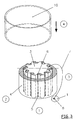
- Figure 1 shows a section through the structure of a transformer according to the invention, wherein the basis for the construction of a printed circuit board 1 of a not shown here device of high-frequency technology.
- a device may be, for example, amplifiers, antenna sockets or the like.
- the circuit board 1 made of an electrically non-conductive material has on its underside (in view of Figure 1) corresponding to the function of the device printed conductors 2. Likewise, the circuit board 1 carries more electrical or electronic components that are required for the function of the device, but have been omitted here for better representability.
- a carrier 3 is automatically placed from an electrically non-conductive material, which is preferably round and has a height required for the function and also has a diameter required for the function. Concentrically around the carrier 3 around a core 4, in particular a ferrite core is arranged, which is also connectable to the circuit board 1. This compound can also be done by a gluing process.
- connection points of the carrier 3 with the printed circuit board 1 are designed as adhesive dots 5 (in particular reflow adhesive dots).
- the carrier 3 On the side facing away from the printed circuit board 1, the carrier 3 has on its upper end side a plurality of contact points 6, which are connected to one end of a winding wire 7 (in particular solderable or bondable). The other end of the winding wire 7 is automatically guided in the direction of the circuit board 1 and connected there to the associated conductor tracks 2.
- the circuit board 1 has on its upper side in the direction of the support 3 contact points 8, which are plated through to the associated conductor tracks 2.
- Figure 2 shows a three-dimensional view of the structure of the transformer according to the invention, in which case only the carrier 3 is shown here for better representability.
- This carrier 3 is located on the printed circuit board 1 and has a plurality of contact points 6 on its upper end side. These contact points 6 on the front side of the carrier 3, as well as the contact points 8 on the circuit board 1, formed as a coating of an electrically conductive material.
- these contact points 6, 8 in a simple manner and quickly applied to the electrically non-conductive material of the circuit board 1 and the support 3 and are then available for later automated contacting to disposal.
- the carrier 3 has grooves 9 corresponding to the number of winding wires 7 for accommodating one winding wire 7 in each case.
- the grooves 9 have the function that the winding wires lying there 7 come to rest behind the outer surface of the carrier 3 so that they do not get in contact with the over the carrier 3 slipped core 4, so that an electrical short circuit is avoided. In addition, reduced by the recessed position of the winding wires 7 in the grooves 9 an undesirable Windungskapaztician.
- winding wires can also be thought of a metallic coating of the contact carrier 3, said coating takes over the function of the winding wire.
- the grooves 9 can be omitted and the coating can be applied directly to the outer surface of the contact carrier 3.
- the gap must be dimensioned so that no contact between the coating and the core 4 is possible.
- winding wire in the claims also means an electrically conductive coating.
- FIG. 3 shows the assembly steps for the production of the transformer according to the invention.
- the carrier 3 is connected to the printed circuit board 1, in particular the conductive compound (5) produced (preferably in the reflow process).
- the core 4 is slipped over, while then in the manufacturing step 3, the electrical connection of the contact points 6 and 8 can be done by means of the winding wires 7. This takes place by means of automatic pick and place machines, in particular with bond machines.
- the finished transformer can still be provided with a cover 10 in order to protect the transmitter from external influences.
- This cover 10 may optionally be glued to the surface of the circuit board 1 or in any other way (releasably, such as non-positively or positively by means of a locking or clip connection, or insoluble) attached.
- the cover 10 shown in Figure 3 is only schematic shown.
- the inner diameter of this cover 10 depends on the outer diameter of the core 4 and, if necessary. Of the winding wires resting there 7. As a rule, a gap between the cover 10 (inside) and core 4 (outside), which should be kept as small as possible.
- the clear inner height of the cover 10 depends on the height of the core 4 and the contact carrier 3, if necessary. Again, taking into account the winding wires 7 and their attachment (for example, Löt- or Bontician on the contact surface).
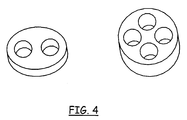
- FIG. 4 shows that the core (4) is designed to accommodate more than one carrier (3) as a double-hole core or multi-hole core (with four holes, for example).
Landscapes
- Engineering & Computer Science (AREA)
- Power Engineering (AREA)
- Coils Or Transformers For Communication (AREA)
Priority Applications (1)
| Application Number | Priority Date | Filing Date | Title |
|---|---|---|---|
| EP05010551A EP1744332A1 (fr) | 2005-07-11 | 2005-07-11 | Translateur à haute fréquence fabriqué automatiquement |
Applications Claiming Priority (1)
| Application Number | Priority Date | Filing Date | Title |
|---|---|---|---|
| EP05010551A EP1744332A1 (fr) | 2005-07-11 | 2005-07-11 | Translateur à haute fréquence fabriqué automatiquement |
Publications (1)
| Publication Number | Publication Date |
|---|---|
| EP1744332A1 true EP1744332A1 (fr) | 2007-01-17 |
Family
ID=37507428
Family Applications (1)
| Application Number | Title | Priority Date | Filing Date |
|---|---|---|---|
| EP05010551A Withdrawn EP1744332A1 (fr) | 2005-07-11 | 2005-07-11 | Translateur à haute fréquence fabriqué automatiquement |
Country Status (1)
| Country | Link |
|---|---|
| EP (1) | EP1744332A1 (fr) |
Citations (11)
| Publication number | Priority date | Publication date | Assignee | Title |
|---|---|---|---|---|
| US4103267A (en) * | 1977-06-13 | 1978-07-25 | Burr-Brown Research Corporation | Hybrid transformer device |
| EP0175069A1 (fr) * | 1984-09-20 | 1986-03-26 | Vacuumschmelze GmbH | Fabrication d'un élément inductif muni d'un noyau toroidal bobiné |
| JPS61191005A (ja) * | 1985-02-20 | 1986-08-25 | Murata Mfg Co Ltd | インダクタンス装置 |
| US4724603A (en) * | 1985-08-13 | 1988-02-16 | Commissariat A L'energie Atomique | Process for producing a toroidal winding of small dimensions and optimum geometry |
| WO1998056016A1 (fr) * | 1997-06-02 | 1998-12-10 | Vacuumschmelze Gmbh | Composant inductif |
| DE19815852A1 (de) * | 1998-04-08 | 1999-10-21 | Vacuumschmelze Gmbh | Trägerkörper für elektronische Bauelemente |
| EP1104931A2 (fr) * | 1999-11-25 | 2001-06-06 | VOGT electronic AG | Noyau annulaire modifié pour un composant électromagnétique |
| US6292081B1 (en) * | 1999-10-28 | 2001-09-18 | Scientific-Atlanta, Inc. | Tunable surface mount toroidal inductor |
| US20020048159A1 (en) * | 2000-10-24 | 2002-04-25 | Wei-Chun Tsao | Surface-mountable impedance device |
| JP2002359119A (ja) * | 2001-05-30 | 2002-12-13 | Fujitsu Denso Ltd | 電子部品 |
| US6662431B1 (en) * | 1997-08-06 | 2003-12-16 | Halo Electronics, Inc. | Electronic surface mount package |
-
2005
- 2005-07-11 EP EP05010551A patent/EP1744332A1/fr not_active Withdrawn
Patent Citations (11)
| Publication number | Priority date | Publication date | Assignee | Title |
|---|---|---|---|---|
| US4103267A (en) * | 1977-06-13 | 1978-07-25 | Burr-Brown Research Corporation | Hybrid transformer device |
| EP0175069A1 (fr) * | 1984-09-20 | 1986-03-26 | Vacuumschmelze GmbH | Fabrication d'un élément inductif muni d'un noyau toroidal bobiné |
| JPS61191005A (ja) * | 1985-02-20 | 1986-08-25 | Murata Mfg Co Ltd | インダクタンス装置 |
| US4724603A (en) * | 1985-08-13 | 1988-02-16 | Commissariat A L'energie Atomique | Process for producing a toroidal winding of small dimensions and optimum geometry |
| WO1998056016A1 (fr) * | 1997-06-02 | 1998-12-10 | Vacuumschmelze Gmbh | Composant inductif |
| US6662431B1 (en) * | 1997-08-06 | 2003-12-16 | Halo Electronics, Inc. | Electronic surface mount package |
| DE19815852A1 (de) * | 1998-04-08 | 1999-10-21 | Vacuumschmelze Gmbh | Trägerkörper für elektronische Bauelemente |
| US6292081B1 (en) * | 1999-10-28 | 2001-09-18 | Scientific-Atlanta, Inc. | Tunable surface mount toroidal inductor |
| EP1104931A2 (fr) * | 1999-11-25 | 2001-06-06 | VOGT electronic AG | Noyau annulaire modifié pour un composant électromagnétique |
| US20020048159A1 (en) * | 2000-10-24 | 2002-04-25 | Wei-Chun Tsao | Surface-mountable impedance device |
| JP2002359119A (ja) * | 2001-05-30 | 2002-12-13 | Fujitsu Denso Ltd | 電子部品 |
Non-Patent Citations (2)
| Title |
|---|
| PATENT ABSTRACTS OF JAPAN vol. 011, no. 020 (E - 472) 20 January 1987 (1987-01-20) * |
| PATENT ABSTRACTS OF JAPAN vol. 2003, no. 04 2 April 2003 (2003-04-02) * |
Similar Documents
| Publication | Publication Date | Title |
|---|---|---|
| DE102016210746B4 (de) | Induktives Bauelement, stromkompensierte Drossel und Verfahren zum Herstellen eines induktiven Bauelements | |
| DE10048290A1 (de) | Induktiver Sensor | |
| EP2388555B1 (fr) | Capteur inductif et son procédé de montage | |
| WO2005045992A1 (fr) | Composant miniature inductif, notamment antenne | |
| DE69907624T2 (de) | Elektromechanische Schaltvorrichtung mit kontrollierter Impedanzumgebung | |
| EP1393604B1 (fr) | Carte de circuits imprimes sur laquelle un connecteur femelle est monte | |
| EP3435482A1 (fr) | Liaison de connexion comprenant un système de câble et un système de plaque, et système de plaque pour une liaison de connexion, procédé de fabrication d'une telle liaison de connexion | |
| EP2609653A1 (fr) | Élément de contact pour le raccordement d'un support de circuit et support de circuit comprenant un élément de contact | |
| DE2828146A1 (de) | Elektrische leiterplatte | |
| WO2008128912A1 (fr) | Composant électronique | |
| EP3345198B1 (fr) | Dispositif haute tension et son procédé de fabrication | |
| DE3403535C2 (fr) | ||
| DE202013010951U1 (de) | Baugruppe zur Leiterplattenbestückung | |
| DE102007035794A1 (de) | Leiterplattenverbund sowie Verfahren zum Herstellen eines Leiterplattenverbundes | |
| DE102004025212B4 (de) | Vollautomatisch fertigbarer Hochfrequenz-Übertrager | |
| EP1744332A1 (fr) | Translateur à haute fréquence fabriqué automatiquement | |
| DE10124117C2 (de) | Leiterplatine mit kontaktiertem SMD-Baustein sowie zugehöriger SMD-Baustein | |
| DE102019132852B4 (de) | Verfahren zum Herstellen eines Leiterstrukturelements und Leiterstrukturelement | |
| EP1598839B1 (fr) | Translateur pour dispositif à haute fréquence placé sur un circuit imprimé | |
| DE10105416A1 (de) | Spule | |
| DE3227645A1 (de) | Elektronisches bauelement und verfahren zu dessen herstellung | |
| EP3627634B1 (fr) | Connecteur enfichable électrique pour un câble électrique multi-fils | |
| DE19652039A1 (de) | Transformator | |
| DE2148475C3 (de) | Hochfrequenzspule mit einer Drahtwicklung und einem gedruckten Wicklungsteil mit einer Anzapfung | |
| DE19615432A1 (de) | Montageplatte |
Legal Events
| Date | Code | Title | Description |
|---|---|---|---|
| PUAI | Public reference made under article 153(3) epc to a published international application that has entered the european phase |
Free format text: ORIGINAL CODE: 0009012 |
|
| AK | Designated contracting states |
Kind code of ref document: A1 Designated state(s): AT BE BG CH CY CZ DE DK EE ES FI FR GB GR HU IE IS IT LI LT LU MC NL PL PT RO SE SI SK TR |
|
| AX | Request for extension of the european patent |
Extension state: AL BA HR LV MK YU |
|
| AKX | Designation fees paid | ||
| STAA | Information on the status of an ep patent application or granted ep patent |
Free format text: STATUS: THE APPLICATION IS DEEMED TO BE WITHDRAWN |
|
| 18D | Application deemed to be withdrawn |
Effective date: 20070717 |
|
| REG | Reference to a national code |
Ref country code: DE Ref legal event code: 8566 |