EP1746430A1 - Orthogonale Fluxgate-Magnetfeldsensor - Google Patents
Orthogonale Fluxgate-Magnetfeldsensor Download PDFInfo
- Publication number
- EP1746430A1 EP1746430A1 EP05405451A EP05405451A EP1746430A1 EP 1746430 A1 EP1746430 A1 EP 1746430A1 EP 05405451 A EP05405451 A EP 05405451A EP 05405451 A EP05405451 A EP 05405451A EP 1746430 A1 EP1746430 A1 EP 1746430A1
- Authority
- EP
- European Patent Office
- Prior art keywords
- excitation
- pick
- coil
- magnetic field
- sensor
- Prior art date
- Legal status (The legal status is an assumption and is not a legal conclusion. Google has not performed a legal analysis and makes no representation as to the accuracy of the status listed.)
- Withdrawn
Links
- 230000005291 magnetic effect Effects 0.000 title claims abstract description 56
- 230000005284 excitation Effects 0.000 claims abstract description 75
- 238000005253 cladding Methods 0.000 claims abstract description 37
- 239000004020 conductor Substances 0.000 claims abstract description 27
- 239000000696 magnetic material Substances 0.000 claims abstract description 14
- 230000005294 ferromagnetic effect Effects 0.000 claims description 44
- 239000000758 substrate Substances 0.000 claims description 15
- 238000000034 method Methods 0.000 claims description 10
- 238000012545 processing Methods 0.000 claims description 8
- 230000008021 deposition Effects 0.000 claims description 5
- 230000008569 process Effects 0.000 claims description 5
- 238000000059 patterning Methods 0.000 claims 1
- 239000003302 ferromagnetic material Substances 0.000 abstract description 6
- 238000004519 manufacturing process Methods 0.000 description 12
- 230000035699 permeability Effects 0.000 description 8
- 238000001514 detection method Methods 0.000 description 7
- 238000009713 electroplating Methods 0.000 description 7
- 238000005516 engineering process Methods 0.000 description 7
- 230000035945 sensitivity Effects 0.000 description 7
- 238000000206 photolithography Methods 0.000 description 6
- 239000004065 semiconductor Substances 0.000 description 6
- 230000007423 decrease Effects 0.000 description 5
- 238000005530 etching Methods 0.000 description 5
- 239000000463 material Substances 0.000 description 5
- 230000008859 change Effects 0.000 description 4
- 239000010949 copper Substances 0.000 description 4
- 230000005347 demagnetization Effects 0.000 description 4
- 238000000151 deposition Methods 0.000 description 4
- 229910000889 permalloy Inorganic materials 0.000 description 4
- 238000009987 spinning Methods 0.000 description 4
- RYGMFSIKBFXOCR-UHFFFAOYSA-N Copper Chemical compound [Cu] RYGMFSIKBFXOCR-UHFFFAOYSA-N 0.000 description 3
- 230000008901 benefit Effects 0.000 description 3
- 229910052802 copper Inorganic materials 0.000 description 3
- 238000010586 diagram Methods 0.000 description 3
- 230000007246 mechanism Effects 0.000 description 3
- 230000000737 periodic effect Effects 0.000 description 3
- VYPSYNLAJGMNEJ-UHFFFAOYSA-N Silicium dioxide Chemical compound O=[Si]=O VYPSYNLAJGMNEJ-UHFFFAOYSA-N 0.000 description 2
- 230000015572 biosynthetic process Effects 0.000 description 2
- 230000000694 effects Effects 0.000 description 2
- 230000010354 integration Effects 0.000 description 2
- 238000001465 metallisation Methods 0.000 description 2
- 238000004544 sputter deposition Methods 0.000 description 2
- 238000004804 winding Methods 0.000 description 2
- 229910000838 Al alloy Inorganic materials 0.000 description 1
- 229910000881 Cu alloy Inorganic materials 0.000 description 1
- CWYNVVGOOAEACU-UHFFFAOYSA-N Fe2+ Chemical compound [Fe+2] CWYNVVGOOAEACU-UHFFFAOYSA-N 0.000 description 1
- 101150081099 OGA gene Proteins 0.000 description 1
- XUIMIQQOPSSXEZ-UHFFFAOYSA-N Silicon Chemical compound [Si] XUIMIQQOPSSXEZ-UHFFFAOYSA-N 0.000 description 1
- 238000005452 bending Methods 0.000 description 1
- 239000000919 ceramic Substances 0.000 description 1
- 229910052681 coesite Inorganic materials 0.000 description 1
- 238000010276 construction Methods 0.000 description 1
- 229910052906 cristobalite Inorganic materials 0.000 description 1
- 238000013461 design Methods 0.000 description 1
- 230000008020 evaporation Effects 0.000 description 1
- 238000001704 evaporation Methods 0.000 description 1
- 230000004907 flux Effects 0.000 description 1
- 239000011521 glass Substances 0.000 description 1
- 239000011810 insulating material Substances 0.000 description 1
- 238000009413 insulation Methods 0.000 description 1
- 238000002955 isolation Methods 0.000 description 1
- 238000005259 measurement Methods 0.000 description 1
- 230000003446 memory effect Effects 0.000 description 1
- 239000007769 metal material Substances 0.000 description 1
- 230000004048 modification Effects 0.000 description 1
- 238000012986 modification Methods 0.000 description 1
- 238000009659 non-destructive testing Methods 0.000 description 1
- 230000003071 parasitic effect Effects 0.000 description 1
- 229920002120 photoresistant polymer Polymers 0.000 description 1
- 230000035939 shock Effects 0.000 description 1
- 229910052710 silicon Inorganic materials 0.000 description 1
- 239000010703 silicon Substances 0.000 description 1
- 239000000377 silicon dioxide Substances 0.000 description 1
- 229910052682 stishovite Inorganic materials 0.000 description 1
- 229910052905 tridymite Inorganic materials 0.000 description 1
Images


Classifications
-
- G—PHYSICS
- G01—MEASURING; TESTING
- G01R—MEASURING ELECTRIC VARIABLES; MEASURING MAGNETIC VARIABLES
- G01R33/00—Arrangements or instruments for measuring magnetic variables
- G01R33/02—Measuring direction or magnitude of magnetic fields or magnetic flux
- G01R33/04—Measuring direction or magnitude of magnetic fields or magnetic flux using the flux-gate principle
-
- G—PHYSICS
- G01—MEASURING; TESTING
- G01R—MEASURING ELECTRIC VARIABLES; MEASURING MAGNETIC VARIABLES
- G01R15/00—Details of measuring arrangements of the types provided for in groups G01R17/00 - G01R29/00, G01R33/00 - G01R33/26 or G01R35/00
- G01R15/14—Adaptations providing voltage or current isolation, e.g. for high-voltage or high-current networks
- G01R15/18—Adaptations providing voltage or current isolation, e.g. for high-voltage or high-current networks using inductive devices, e.g. transformers
- G01R15/183—Adaptations providing voltage or current isolation, e.g. for high-voltage or high-current networks using inductive devices, e.g. transformers using transformers with a magnetic core
- G01R15/185—Adaptations providing voltage or current isolation, e.g. for high-voltage or high-current networks using inductive devices, e.g. transformers using transformers with a magnetic core with compensation or feedback windings or interacting coils, e.g. 0-flux sensors
Definitions
- the present invention relates to an integrated orthogonal fluxgate magnetic sensor and method of the fabrication thereof.
- Fluxgates are the most popular, high sensitivity magnetic sensors built using an easily saturable ferromagnetic core. Fluxgate type magnetic sensors may be used for magnitudinal and directional measurement of DC or low-frequency AC magnetic fields. Typical applications are electronic compasses, current sensors, magnetic ink reading, detection of ferrous materials, and non-destructive testing [1, 2]. The main advantage of fluxgate sensors are their high sensitivity and very low offset. On the other hand, low magnetic field operation range and high perming are problems in current fluxgate sensors [3].
- fluxgate sensors based on the periodic saturation of ferromagnetic material with an AC excitation field and to detect the change in the flux passing through the core, which is proportional to the external magnetic field.
- Two kinds of configurations in fluxgates are generally known: a parallel fluxgate, having the excitation field parallel to the measured field, and an orthogonal fluxgate with the excitation field perpendicular to the measured field.
- only one ferromagnetic core combined with coils can be used as a fluxgate sensor.
- the orthogonal fluxgate configuration is preferable because of better signal treatment dynamic of the fluxgate sensor.
- the magnetic field to be measured is physically decoupled from the excitation field by placing the sensing coil to the orthogonal position with respect to the excitation field. The contribution of the excitation field is then removed from the measured signal [6].
- Figure 1 illustrates an orthogonal configuration of a conventional single-core fluxgate sensor.
- the circular excitation magnetic field Hexc is orthogonal to the axis of the core (C) and consequently to the external applied magnetic field Hext.
- Such an arrangement decouples the sensing coil (S) from the excitation coil (E).
- the conventional orthogonal fluxgate sensor shown in Figure 1 is however costly to manufacture, particularly in view of the need to wind the excitation coil around the ferromagnetic core, a portion of the coil being fed through the central cavity provided in the core. Winding of the sensing coil around the core is also not particularly cost effective. The excitation coil winding also limits the practical length thereof. The construction also limits the degree of miniaturization and the possibilities of integration of the sensor in miniaturized electronic devices.
- An object of this invention is to provide an orthogonal fluxgate sensor that is compact, cost effective to manufacture in industrial series, and that demonstrates good performance, in particular a wide measuring range, low perming effect, and high precision.
- an orthogonal fluxgate magnetic field sensor comprising an excitation conductor made of a non-magnetic conducting material, a saturable magnetic material, and at least one pick-up coil, wherein the excitation conductor comprises an essentially linear portion in the form of a rod, clad therealong and therearound by the saturable magnetic material.
- the one or more pick-up coils are preferably arranged adjacent ends of the ferromagnetic cladding.
- the ferromagnetic cladding may be in direct contact with the excitation conductor without insulation therebetween.
- the ferromagnetic cladding and excitation conductor may be formed by deposition and etching of layers that are built up to form an integrated structure, such as a LiGA process with copper electroplating and etching for non-magnetic conductor formation, and ferromagnetic permalloy deposition for the cladding.
- the layers may be built up on a silicon substrate in which the sensor drive and control electronic circuit is also integrated, such as a case of a CMOS process.
- the sensor configuration according to the invention significantly decreases the sensor size and footprint and can be manufactured by integrated circuit layer build-up processes, whereby the sensor drive and signal processing circuitry may be directly provided in the semiconductor substrate to provide a very compact, low cost and low power consuming magnetic field sensor.
- a further important advantage of the sensor according to the invention is the even saturation of the ferromagnetic cladding surrounding the center excitation conductor over the entire length of the cladding.
- the length of the center excitation conductor and cladding can be varied easily from one sensor design to another, in order to change the sensitivity and operating range of the sensor without any significant changes to the manufacturing process.
- excitation conductor and sensing coils are separately driven, and independent, thereby ensuring high sensor signal to noise ratio and stability.
- a single conducting rod going through the center of the saturable ferromagnetic cladding drastically decreases the required semiconductor surface occupied by the excitation mechanism, compared with prior integrated fluxgate sensors containing planar excitation coils.
- An excitation current I exc fed via electric contacts, for example realized by electroplating and flowing along the center conducting layer, produces a circular magnetic field H exc .
- the longitudinal magnetic permeability i.e. in the direction parallel to the measuring field
- H cir perpendicular to the measuring field.
- Two sensing elements represented by the pick-up coils or alternatively by Hall plate elements positioned below opposite longitudinal ends of the ferromagnetic cladding are used for the detection of an alternating magnetic field that is proportional to the external magnetic field H ext .
- the cross-section shape of the ferromagnetic cladding and the central excitation conductor is preferably square or circular, but may have other forms.
- the perimeter of the ferromagnetic core is preferably reduced down to minimum size allowed by the layer deposition technology.
- the center of the each portion of pick-up coil is located under the longitudinal end of the ferromagnetic cladding where the field concentration in the direction perpendicular to the substrate is the highest.
- the ferromagnetic cladding, the sensing coil and the substrate are isolated from each other by non-conducting, non-magnetic material.
- the electrical isolation between the central excitation conductor and the ferromagnetic cladding is not necessary, but could be provided, if desired.
- High linearity of the microsensor can be achieved by introducing a feedback configuration to the system.
- Either planar coils positioned under the ferromagnetic structure or an external discrete coil around the microsensor is the element generating the compensation field.
- the planar coil for the feedback can be the same as that for the signal sensing.
- This magnetic sensor can be combined with an electronic circuit made in CMOS technology.
- the electronics may advantageously provide all the necessary signals for excitation, signal detection and feedback.
- the different direction of the circular excitation H cir from the longitudinal measured field H ext , to which the cylindrical ferromagnetic structure is exposed, is very advantageous.
- the orthogonal configuration of fluxgate sensor since the orthogonal configuration of fluxgate sensor is used, the contribution of the excitation field is removed from the measured signal.
- the magnetic structure has a closed path and the ferromagnetic cladding layer with apparent permeability ⁇ a equal to intrinsic permeability ⁇ i is directly exposed to the circular excitation field H cir . Consequently, the level of the excitation field H cir necessary to reach the cladding saturation stays unchanged while changing the length I of the ferromagnetic cladding. Therefore, the length I of the structure has no impact on the excitation mechanism.
- the measuring range of the sensor can thus easily be adjusted by simply changing the excitation conductor and cladding structure length I.
- the excitation rod is coated with the ferromagnetic material in a way that a circular magnetic excitation field loop is formed inside the ferromagnetic material.
- the permeability of the ferromagnetic layer is periodically modulated in the orthogonal direction with respect to the measured magnetic field by passing an AC current through the excitation rod. This makes the detection part independent of the excitation mechanism and the measuring range and the sensitivity can be adjusted by modifying only the cladding length.
- the modification of the core length changes the demagnetization factor [5] of the core.
- the apparent relative permeability ⁇ app of the core deviates from its intrinsic value according to the demagnetization factor.
- ⁇ app ⁇ i 1 + N ⁇ ⁇ i ⁇ 1
- ⁇ i the intrinsic relative permeability
- N the demagnetization factor
- the geometry in the radial direction, i.e. in the excitation direction the geometry can be considered as an infinitely long magnetic material core due to the closed magnetic loop, for which the demagnetization factor is zero. So, the slope of the B-H curve is a maximum, which allows easy and homogenous saturation along the whole cladding length.
- an orthogonal fluxgate magnetic field sensor 2 comprises an excitation conductor 4 having an essentially linear portion 6, hereinafter referred to as "excitation rod" clad with a saturable ferromagnetic cladding 8, and a sensor pick-up coil 10 having coil portions 12 arranged adjacent opposed ends 14 of the saturable ferromagnetic cladding 8.
- the sensor further comprises a substrate 16 on which the cladding 8 and excitation conductor 4 are mounted.
- the substrate 16 may be made of a ceramic, glass or other insulating material.
- the substrate 16 is made of a semi-conductor material comprising an integrated circuit including the pick-up coil 10 and connected to the excitation conductor 4. Exemplary embodiments of circuits that may be integrated in the semiconductor are illustrated in the block diagrams of Figures 4a and 4b, that will be described further on.
- the sensing coil and excitation conductor may be provided with respective conducting pads 18, 20 (see figure 2a) for bonding to electrical conductors connected to an external signal processing and excitation circuit.
- the substrate 16 comprises an integrated circuit, as schematically illustrated by the layer 16a in Figure 3, ends 20 of the excitation conductor may be directly interconnected to the circuit by vias 21 created during layer deposition of the conductor.
- the interconnections of the pick-up coil between different layers, respectively to the circuit may be performed through vias or contact points 23.
- the substrate 16 with integrated circuit 16a may be made of other known semiconductor technologies, such as CMOS, in which case the semiconductor layer with integrated circuit and metallic conducting layers forming the pick-up coils could be directly integrated in the substrate resulting in an integrated circuit composed of 16a, 15 and 13, the magnetic material and excitation conductor being deposited thereon. An example of the manufacturing procedure will be described further on.
- the sensing coil 10 is preferably planar, whereby the coil portions 12 have their centers approximately situated at respective ends 14 of the ferromagnetic cladding 8. This ensures the maximum pick-up of the external magnetic field orthogonal to the plane of the substrate due to the bending of the external magnetic field lines into the ferromagnetic cladding, the concentration being greatest at the extremities 14.
- each coil portion 12 may be formed of two sets of spirals 12a, 12b provided on two stacked layers 13, 15, as shown in Figure 3, thereby doubling the number of turns of the sensing coil. Since two layers would normally be required for the sensing coil in order to route the connection points 18 outside of the center of the coils for practical purposes, the additional coil does not add any layers and therefore does not complicate the manufacturing process. Yet further layers could be added, if greater measuring sensitivity is required.
- the cladding 8 is preferably formed of a ferromagnetic material such as a material commonly known as "permalloy", although other soft magnetic materials that are easily saturable and that have low hysteresis may be used.
- a ferromagnetic material such as a material commonly known as "permalloy", although other soft magnetic materials that are easily saturable and that have low hysteresis may be used.
- the advantage of ferromagnetic materials is that they are easy to deposit in an advantageous manufacturing method for building the sensor according to this invention.
- the material used for the excitation conductor portion and the pick-up coil is preferably copper, or copper alloy, although other non-magnetic materials with good conductive properties may be used.
- a clock signal Clk with a frequency f o is generated by a generator GEN.
- the frequency of the signal is divided by 2 and the signal is converted by the driver into a voltage waveform having only odd harmonics and zero offset such as a sinusoidal, triangular, or pulsed waveform.
- This voltage waveform is converted into a current waveform and fed to the excitation rod of the ferromagnetic core.
- the level of the current waveform must be high enough to saturate the ferromagnetic core. This periodic saturation produces an induced voltage proportional to the external magnetic field H ext , across the terminals of the pick-up coils placed below the edges of the core.
- the induced voltage is amplified and synchronously rectified by the demodulator DEM. Then the resulting signal is fed to a low pass filter with cut-off frequency lower than f o .
- the output of the low pass filter is a DC voltage proportional to the external magnetic field H ext within the measuring range of the sensor.
- a clock signal Clk with a frequency f o is generated by a generator GEN.
- the frequency of the signal is divided by 2 and the signal is converted by the driver into a voltage waveform having only odd harmonics and zero offset such as a sinusoidal, triangular, or pulsed waveform.
- This voltage waveform is converted into a current waveform and fed to the excitation rod of the ferromagnetic core.
- the level of the current waveform must be high enough to saturate the ferromagnetic core. This periodic saturation produces an induced voltage proportional to the external magnetic field H ext , across the terminals of the pick-up coils placed below the edges of the core.
- the induced voltage is amplified and synchronously rectified by the demodulator DEM. Then the signal is integrated in an integrator and passed through a voltage to current converter. The resulting current is fed to the feedback coil which produces a compensating magnetic field H comp in the opposite direction of the external magnetic field H ext , resulting in a decrease in the induced voltage across the terminals of the pick-up coils.
- the current passing through the feedback coil produces the same level of the magnetic field as the external field, so that the total field around the core is zero and no voltage is induced across the pick-up coils. This makes the outputs of the amplifier and the demodulator also zero, and the output of the integrator is a DC voltage proportional to the external magnetic field H ext .
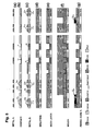
- Figure 5 illustrates the sequence of steps in the build-up of layers in an example of the process steps in manufacturing a sensor according to the invention.
- the left hand section of Figure 5 shows a representative longitudinal cross-section through the sensor layers, whereas the right hand sight is representative of a transverse cross-section.
- a lower layer of the pick-up coils 12a and contact pads 20 for the excitation rod are formed on the substrate by known metal deposition techniques such as sputtering, followed by photolithography and etching to form the pattern, whereby the deposited metal material is for example an aluminum alloy AISi1%.
- step (b) a contact layer is deposited, for example SiO 2 , by sputtering, followed by photolithography and etching, to form the patterns, in particular to free the vias 21,23 for interconnection of the two layers of the pick-up coil 12a, 12b, the second coil layer 12b being deposited in step (c) by the same techniques as in step (a).
- a contact layer for example SiO 2 , by sputtering, followed by photolithography and etching, to form the patterns, in particular to free the vias 21,23 for interconnection of the two layers of the pick-up coil 12a, 12b, the second coil layer 12b being deposited in step (c) by the same techniques as in step (a).
- step (d) an insulating layer, for example SU-8, is deposited by spinning, followed by photolithography over which a seed layer for electroplating is deposited in step (e), for example Cr/Cu by evaporation.
- a seed layer for electroplating is deposited in step (e), for example Cr/Cu by evaporation.
- step (f) a mold [4], for example AZ9260, is deposited on the layers by spinning followed by photolithography, leaving exposed the openings required for forming a base portion 8a of the ferromagnetic cladding, for example Permalloy (Fe 19 Ni 81 ), which is deposited by electroplating and the mold removed as shown in step (g).
- a mold [4] for example AZ9260
- AZ9260 AZ9260
- step (h) a further mold is is deposited by spinning followed by photolithography to allow formation of the conductive excitation rod 6 by electroplating copper and subsequently removing the mold as shown in step (i).
- the excitation rod is connected to vias 21 for connection to the drive circuit.
- step (j) a mold is deposited by spinning followed by photolithography, around the partially formed ferromagnetic base layer 8a and the excitation rod 6 to allow electroplating of the remaining part of the ferromagnetic cladding 8 around the excitation rod, as shown in step (k).
- step (I) the seed layer remaining exposed is removed by etching.
- the pick-up coil may already be integrated in the integrated circuit, in other words, the equivalent of steps (a) to (d) would already be integrated in the CMOS fabrication technology, the additional process steps starting from creation of the seed layer from step (e) onwards.
Landscapes
- Physics & Mathematics (AREA)
- Condensed Matter Physics & Semiconductors (AREA)
- General Physics & Mathematics (AREA)
- Measuring Magnetic Variables (AREA)
Priority Applications (6)
| Application Number | Priority Date | Filing Date | Title |
|---|---|---|---|
| EP05405451A EP1746430A1 (de) | 2005-07-22 | 2005-07-22 | Orthogonale Fluxgate-Magnetfeldsensor |
| EP06779889A EP1907872A1 (de) | 2005-07-22 | 2006-07-17 | Orthogonal-fluxgate-magnetfeldsensor |
| US11/989,184 US7834620B2 (en) | 2005-07-22 | 2006-07-17 | Orthogonal fluxgate magnetic field sensor |
| JP2008522085A JP2009503443A (ja) | 2005-07-22 | 2006-07-17 | 直交フラックスゲート式磁界センサー |
| CNA2006800268697A CN101228453A (zh) | 2005-07-22 | 2006-07-17 | 正交磁通门磁场传感器 |
| PCT/IB2006/002007 WO2007010378A1 (en) | 2005-07-22 | 2006-07-17 | Orthogonal fluxgate magnetic field sensor |
Applications Claiming Priority (1)
| Application Number | Priority Date | Filing Date | Title |
|---|---|---|---|
| EP05405451A EP1746430A1 (de) | 2005-07-22 | 2005-07-22 | Orthogonale Fluxgate-Magnetfeldsensor |
Publications (1)
| Publication Number | Publication Date |
|---|---|
| EP1746430A1 true EP1746430A1 (de) | 2007-01-24 |
Family
ID=36001158
Family Applications (2)
| Application Number | Title | Priority Date | Filing Date |
|---|---|---|---|
| EP05405451A Withdrawn EP1746430A1 (de) | 2005-07-22 | 2005-07-22 | Orthogonale Fluxgate-Magnetfeldsensor |
| EP06779889A Withdrawn EP1907872A1 (de) | 2005-07-22 | 2006-07-17 | Orthogonal-fluxgate-magnetfeldsensor |
Family Applications After (1)
| Application Number | Title | Priority Date | Filing Date |
|---|---|---|---|
| EP06779889A Withdrawn EP1907872A1 (de) | 2005-07-22 | 2006-07-17 | Orthogonal-fluxgate-magnetfeldsensor |
Country Status (5)
| Country | Link |
|---|---|
| US (1) | US7834620B2 (de) |
| EP (2) | EP1746430A1 (de) |
| JP (1) | JP2009503443A (de) |
| CN (1) | CN101228453A (de) |
| WO (1) | WO2007010378A1 (de) |
Cited By (8)
| Publication number | Priority date | Publication date | Assignee | Title |
|---|---|---|---|---|
| EP2037286A1 (de) * | 2007-09-13 | 2009-03-18 | Micronas GmbH | Messvorrichtung zur Messung eines magnetischen Felds |
| US20140327434A1 (en) * | 2011-09-09 | 2014-11-06 | Kyushu University, National University Corporation | Magnetic field sensor |
| FR3060757A1 (fr) * | 2016-12-19 | 2018-06-22 | Safran Electronics & Defense | Capteur de courant a vanne de flux |
| EP3514559A1 (de) * | 2018-01-22 | 2019-07-24 | Melexis Technologies SA | Sensorpaket |
| US10845215B2 (en) | 2018-01-22 | 2020-11-24 | Melexis Technologies Sa | Inductive position sensor |
| AT522600A1 (de) * | 2019-04-15 | 2020-12-15 | Braunschmid Dipl Ing Msc Franz | Flachspule für drahtlose Energieübertragung |
| CN112384812A (zh) * | 2018-06-27 | 2021-02-19 | 赛峰电子与防务公司 | 具有磁通门的电流传感器 |
| CN120405207A (zh) * | 2025-07-01 | 2025-08-01 | 北京智芯微电子科技有限公司 | 电流传感芯片及制造方法 |
Families Citing this family (30)
| Publication number | Priority date | Publication date | Assignee | Title |
|---|---|---|---|---|
| EP2071346A1 (de) * | 2007-12-14 | 2009-06-17 | Liaisons Electroniques-Mecaniques Lem S.A. | Dünnfilm-Fluxgate-Sensor |
| DE102009028956A1 (de) * | 2009-08-28 | 2011-03-03 | Robert Bosch Gmbh | Magnetfeldsensor |
| DE102009044988A1 (de) * | 2009-09-24 | 2011-03-31 | Robert Bosch Gmbh | Leistungsoptimierte Ansteuerung eines Fluxgatesensors |
| US8508218B2 (en) * | 2011-05-11 | 2013-08-13 | Sensima Technology Sa | Hall-effect-based angular orientation sensor and corresponding method |
| US9354257B2 (en) * | 2011-11-04 | 2016-05-31 | General Electric Company | Systems and methods for use in measuring current through a conductor |
| JP5393844B2 (ja) * | 2012-06-08 | 2014-01-22 | 株式会社フジクラ | 磁気素子制御装置、磁気素子制御方法及び磁気検出装置 |
| JP5364816B1 (ja) | 2012-06-08 | 2013-12-11 | 株式会社フジクラ | 磁気素子制御装置、磁気素子制御方法及び磁気検出装置 |
| US9176203B2 (en) | 2013-02-05 | 2015-11-03 | Texas Instruments Incorporated | Apparatus and method for in situ current measurement in a conductor |
| KR20250024862A (ko) | 2013-03-14 | 2025-02-19 | 캘리포니아 인스티튜트 오브 테크놀로지 | 비정상 검출을 위한 방법, 비정상을 검출하기 위한 시스템, 및 에너지 저장 시스템 |
| CN103323794B (zh) * | 2013-06-21 | 2015-07-15 | 中国人民解放军国防科学技术大学 | 一种采用平面微线圈的gmr-mems集成弱磁传感器 |
| RU2533345C1 (ru) * | 2013-06-28 | 2014-11-20 | Федеральное государственное унитарное предприятие "Всероссийский научно-исследовательский институт автоматики им. Н.Л. Духова" (ФГУП "ВНИИА") | Способ измерения амплитуды двухполярного импульса магнитного поля |
| WO2015052059A1 (en) * | 2013-10-07 | 2015-04-16 | Koninklijke Philips N.V. | Precision batch production method for manufacturing ferrite rods |
| CN105745547B (zh) * | 2013-10-17 | 2019-04-05 | 公立大学法人大阪市立大学 | 电流测定装置和电流测定方法 |
| KR101532150B1 (ko) * | 2013-12-09 | 2015-06-26 | 삼성전기주식회사 | 직교형 플럭스게이트 센서 |
| US10389141B2 (en) | 2014-12-19 | 2019-08-20 | California Institute Of Technology | Systems and methods for management and monitoring of energy storage and distribution |
| US10878997B2 (en) | 2015-03-13 | 2020-12-29 | Taiwan Semiconductor Manufacturing Company, Ltd. | Integrated circuit having current-sensing coil |
| CN104808157B (zh) * | 2015-04-11 | 2017-10-24 | 西北工业大学 | 一种印制电路板正交磁通门传感器 |
| US11092656B2 (en) * | 2015-05-12 | 2021-08-17 | Texas Instruments Incorporated | Fluxgate magnetic field detection method and circuit |
| EP3356836B1 (de) | 2015-10-01 | 2022-06-29 | California Institute of Technology | System und verfahren zur überwachung der eigenschaften von energieeinheiten |
| CN105676151B (zh) * | 2016-01-18 | 2018-06-22 | 华东师范大学 | 一种负反馈式磁场传感器 |
| US10184991B2 (en) * | 2016-05-11 | 2019-01-22 | Texas Instruments Incorporated | Dual-axis fluxgate device |
| US11008650B2 (en) | 2016-11-03 | 2021-05-18 | Starfire Industries Llc | Compact system for coupling RF power directly into RF linacs |
| EP3382409B1 (de) * | 2017-03-31 | 2022-04-27 | AT & S Austria Technologie & Systemtechnik Aktiengesellschaft | Baugruppenträger mit integriertem flux-gate-sensor |
| JP7262885B2 (ja) * | 2017-06-16 | 2023-04-24 | 朝日インテック株式会社 | 超高感度マイクロ磁気センサ |
| JP7262886B2 (ja) * | 2017-07-21 | 2023-04-24 | 朝日インテック株式会社 | 超小型高感度磁気センサ |
| CN109358301A (zh) * | 2018-09-29 | 2019-02-19 | 河南理工大学 | 一种基于缝纫式线芯结构的微型磁通门传感器 |
| CN109507474A (zh) * | 2018-12-04 | 2019-03-22 | 上海波卉电源科技有限公司 | 用数控磁通门实现超高精度高低压电流采样技术 |
| CN113474482B (zh) * | 2019-02-25 | 2025-07-15 | 星火工业有限公司 | 用于事故耐受核燃料、粒子加速器、和航空航天前沿的金属和陶瓷纳米涂层的方法和设备 |
| EP3812785A1 (de) * | 2019-10-22 | 2021-04-28 | LEM International SA | Fluxgate-stromwandler |
| CN111123177B (zh) * | 2020-01-20 | 2022-06-17 | 河南理工大学 | 一种折叠形多层铁芯正交磁通门传感器 |
Citations (4)
| Publication number | Priority date | Publication date | Assignee | Title |
|---|---|---|---|---|
| US3218547A (en) * | 1961-11-29 | 1965-11-16 | Ling Sung Ching | Flux sensing device using a tubular core with toroidal gating coil and solenoidal output coil wound thereon |
| US6194897B1 (en) * | 1997-10-06 | 2001-02-27 | Tdk Corporation | Magnetic sensor apparatus |
| EP1293792A2 (de) * | 2001-09-17 | 2003-03-19 | Canon Denshi Kabushiki Kaisha | Magnetisches Detektionselement unter Verwendung des Magnetoimpedanzeffekts, Verfahren zur Herstellung des Elements, und tragbares Gerät mit diesem Element |
| US6690164B1 (en) * | 1999-12-17 | 2004-02-10 | Commissariat A L'energie Atomique | Perpendicular detection fluxgate micromagnetometer and method for the production thereof |
Family Cites Families (2)
| Publication number | Priority date | Publication date | Assignee | Title |
|---|---|---|---|---|
| JPS5024183B1 (de) * | 1970-12-03 | 1975-08-13 | ||
| EP1260825A1 (de) * | 2001-05-25 | 2002-11-27 | Sentron Ag | Magnetfeldsensor |
-
2005
- 2005-07-22 EP EP05405451A patent/EP1746430A1/de not_active Withdrawn
-
2006
- 2006-07-17 EP EP06779889A patent/EP1907872A1/de not_active Withdrawn
- 2006-07-17 CN CNA2006800268697A patent/CN101228453A/zh active Pending
- 2006-07-17 US US11/989,184 patent/US7834620B2/en active Active
- 2006-07-17 WO PCT/IB2006/002007 patent/WO2007010378A1/en not_active Ceased
- 2006-07-17 JP JP2008522085A patent/JP2009503443A/ja not_active Withdrawn
Patent Citations (4)
| Publication number | Priority date | Publication date | Assignee | Title |
|---|---|---|---|---|
| US3218547A (en) * | 1961-11-29 | 1965-11-16 | Ling Sung Ching | Flux sensing device using a tubular core with toroidal gating coil and solenoidal output coil wound thereon |
| US6194897B1 (en) * | 1997-10-06 | 2001-02-27 | Tdk Corporation | Magnetic sensor apparatus |
| US6690164B1 (en) * | 1999-12-17 | 2004-02-10 | Commissariat A L'energie Atomique | Perpendicular detection fluxgate micromagnetometer and method for the production thereof |
| EP1293792A2 (de) * | 2001-09-17 | 2003-03-19 | Canon Denshi Kabushiki Kaisha | Magnetisches Detektionselement unter Verwendung des Magnetoimpedanzeffekts, Verfahren zur Herstellung des Elements, und tragbares Gerät mit diesem Element |
Non-Patent Citations (9)
| Title |
|---|
| F. KALUZA; A. GRUGER; H. GRUGER: "New and future applications of fluxgate sensors", SENSORS & ACTUATORS A, vol. 106, 2003, pages 48 - 51 |
| F. PRIMDAHL: "The fluxgate magnetometer", J. PHYS. E: SCI. INSTRUM., vol. 12, 1979, pages 241 - 253 |
| J. A. OSBORN: "Demagnetizing Factors for the General Ellipsoid", PHYSICAL REVIEW, vol. 67, no. 11 -12, 1 June 1945 (1945-06-01), pages 351 - 357 |
| J. M. QUEMPER: "Permalloy electroplating through photoresist molds", SENSORS & ACTUATORS, vol. A74, 1999, pages 1 - 4 |
| L. CHIESI ET AL.: "CMOS planar 2D micro- fluxgate sensor", SENSORS AND ACTUATORS A: PHYSICAL, vol. 82, no. 1-3, 15 May 2000 (2000-05-15), pages 174 - 180 |
| P. RIPKA: "Advances in fluxgate sensors", SENSORS & ACTUATORS A, vol. 106, 14 August 2003 (2003-08-14) |
| PAVEL RIPKA: "MAGNETIC SENSORS AND MAGNETOMETERS", January 2001, ARTECH HOUSE PUBLISHERS |
| R. GOTTFRIED-GOTTFRIED ET AL.: "A miniaturized magnetic-field sensor system consisting of a planar fluxgate sensor and a CMOS readout circuitry", SENSORS AND ACTUATORS A: PHYSICAL, vol. 54, no. 1- 3, June 1996 (1996-06-01), pages 443 - 447 |
| S. O. CHOI ET AL.: "An integrated micro fluxgate magnetic sensor", SENSORS AND ACTUATORS A: PHYSICAL, vol. 55, no. 2-3, 31 July 1996 (1996-07-31), pages 121 - 126 |
Cited By (18)
| Publication number | Priority date | Publication date | Assignee | Title |
|---|---|---|---|---|
| EP2037286A1 (de) * | 2007-09-13 | 2009-03-18 | Micronas GmbH | Messvorrichtung zur Messung eines magnetischen Felds |
| US8067934B2 (en) | 2007-09-13 | 2011-11-29 | Micronas Gmbh | Measurement device for measuring a magnetic field |
| US20140327434A1 (en) * | 2011-09-09 | 2014-11-06 | Kyushu University, National University Corporation | Magnetic field sensor |
| EP2755040A4 (de) * | 2011-09-09 | 2016-01-20 | Univ Kyushu Nat Univ Corp | Magnetfeldsensor |
| US9285436B2 (en) * | 2011-09-09 | 2016-03-15 | Kyushu University | Magnetic field sensor |
| FR3060757A1 (fr) * | 2016-12-19 | 2018-06-22 | Safran Electronics & Defense | Capteur de courant a vanne de flux |
| WO2018115032A1 (fr) * | 2016-12-19 | 2018-06-28 | Safran Electronics & Defense | Capteur de courant a vanne de flux |
| US10884028B2 (en) | 2016-12-19 | 2021-01-05 | Safran Electronics & Defense | Current sensor with fluxgate |
| CN111556956A (zh) * | 2018-01-22 | 2020-08-18 | 迈来芯电子科技有限公司 | 传感器封装 |
| US10845215B2 (en) | 2018-01-22 | 2020-11-24 | Melexis Technologies Sa | Inductive position sensor |
| EP3514559A1 (de) * | 2018-01-22 | 2019-07-24 | Melexis Technologies SA | Sensorpaket |
| US11002568B2 (en) | 2018-01-22 | 2021-05-11 | Melexis Technologies Sa | Inductive position sensor |
| CN111556956B (zh) * | 2018-01-22 | 2022-12-09 | 迈来芯电子科技有限公司 | 传感器封装 |
| US11733318B2 (en) | 2018-01-22 | 2023-08-22 | Melexis Technologies Sa | Sensor package |
| CN112384812A (zh) * | 2018-06-27 | 2021-02-19 | 赛峰电子与防务公司 | 具有磁通门的电流传感器 |
| AT522600A1 (de) * | 2019-04-15 | 2020-12-15 | Braunschmid Dipl Ing Msc Franz | Flachspule für drahtlose Energieübertragung |
| AT522600B1 (de) * | 2019-04-15 | 2023-03-15 | Braunschmid Dipl Ing Msc Franz | Flachspule für drahtlose Energieübertragung |
| CN120405207A (zh) * | 2025-07-01 | 2025-08-01 | 北京智芯微电子科技有限公司 | 电流传感芯片及制造方法 |
Also Published As
| Publication number | Publication date |
|---|---|
| CN101228453A (zh) | 2008-07-23 |
| WO2007010378A1 (en) | 2007-01-25 |
| US20090230955A1 (en) | 2009-09-17 |
| JP2009503443A (ja) | 2009-01-29 |
| US7834620B2 (en) | 2010-11-16 |
| EP1907872A1 (de) | 2008-04-09 |
Similar Documents
| Publication | Publication Date | Title |
|---|---|---|
| US7834620B2 (en) | Orthogonal fluxgate magnetic field sensor | |
| Liakopoulos et al. | A micro-fluxgate magnetic sensor using micromachined planar solenoid coils | |
| Ripka | Advances in fluxgate sensors | |
| US5831431A (en) | Miniaturized coil arrangement made by planar technology, for the detection of ferromagnetic materials | |
| JP5518661B2 (ja) | 半導体集積回路、磁気検出装置、電子方位計 | |
| KR101267246B1 (ko) | 플럭스 게이트 센서 및 이것을 사용한 전자 방위계 | |
| KR910004261B1 (ko) | 자전 변환 소자를 이용한 검지기 | |
| KR100468833B1 (ko) | 차동스파이어럴형자계검출소자및이를채용한자계검출모듈 | |
| US20040027121A1 (en) | Printed circuit board integrated with a two-axis fluxgate sensor and method for manufacturing the same | |
| JP2008032723A (ja) | 交流磁気励磁を備える改善された電流センサ | |
| WO2011155527A1 (ja) | フラックスゲートセンサおよびそれを利用した電子方位計ならびに電流計 | |
| US7414399B2 (en) | Micromagnetometer of the fluxgate type with improved excitation coil | |
| US6998840B2 (en) | Fluxgate sensor integrated having stacked magnetic cores in printed circuit board and method for manufacturing the same | |
| JP2003004831A (ja) | 直交フラックスゲート型磁気センサ | |
| Ripka et al. | Pulse excitation of micro-fluxgate sensors | |
| WO2010020648A1 (en) | A fluxgate sensor | |
| US20140055131A1 (en) | Magnetic field sensor | |
| Yao et al. | A high-sensitivity MEMS fluxgate sensor with double-layer induction coils fabricated by micro-casting | |
| JPS63253264A (ja) | 電流検出器 | |
| Robertson | Microfabricated fluxgate sensors with low noise and wide bandwidth | |
| Choi et al. | The microfluxgate magnetic sensor having closed magnetic path | |
| Lu et al. | Design, fabrication, and characterization of a 3-D CMOS fluxgate magnetometer | |
| JP2010271081A (ja) | 磁気センサ素子およびそれを用いた電子方位計と磁界検出方法 | |
| Liakopoulos et al. | A micro fluxgate magnetic sensor using micromachined 3-dimensional planar coils | |
| JP2006518845A (ja) | 小型磁場センサ |
Legal Events
| Date | Code | Title | Description |
|---|---|---|---|
| PUAI | Public reference made under article 153(3) epc to a published international application that has entered the european phase |
Free format text: ORIGINAL CODE: 0009012 |
|
| AK | Designated contracting states |
Kind code of ref document: A1 Designated state(s): AT BE BG CH CY CZ DE DK EE ES FI FR GB GR HU IE IS IT LI LT LU LV MC NL PL PT RO SE SI SK TR |
|
| AX | Request for extension of the european patent |
Extension state: AL BA HR MK YU |
|
| AKX | Designation fees paid | ||
| REG | Reference to a national code |
Ref country code: DE Ref legal event code: 8566 |
|
| STAA | Information on the status of an ep patent application or granted ep patent |
Free format text: STATUS: THE APPLICATION IS DEEMED TO BE WITHDRAWN |
|
| 18D | Application deemed to be withdrawn |
Effective date: 20070725 |