EP1746488A2 - Sensoranordnungsstruktur eines elektromagnetischen Digitalisierers - Google Patents
Sensoranordnungsstruktur eines elektromagnetischen Digitalisierers Download PDFInfo
- Publication number
- EP1746488A2 EP1746488A2 EP06117603A EP06117603A EP1746488A2 EP 1746488 A2 EP1746488 A2 EP 1746488A2 EP 06117603 A EP06117603 A EP 06117603A EP 06117603 A EP06117603 A EP 06117603A EP 1746488 A2 EP1746488 A2 EP 1746488A2
- Authority
- EP
- European Patent Office
- Prior art keywords
- sensor
- sensor array
- conductive lines
- segments
- array
- Prior art date
- Legal status (The legal status is an assumption and is not a legal conclusion. Google has not performed a legal analysis and makes no representation as to the accuracy of the status listed.)
- Withdrawn
Links
Images



Classifications
-
- G—PHYSICS
- G06—COMPUTING OR CALCULATING; COUNTING
- G06F—ELECTRIC DIGITAL DATA PROCESSING
- G06F3/00—Input arrangements for transferring data to be processed into a form capable of being handled by the computer; Output arrangements for transferring data from processing unit to output unit, e.g. interface arrangements
- G06F3/01—Input arrangements or combined input and output arrangements for interaction between user and computer
- G06F3/03—Arrangements for converting the position or the displacement of a member into a coded form
- G06F3/041—Digitisers, e.g. for touch screens or touch pads, characterised by the transducing means
- G06F3/046—Digitisers, e.g. for touch screens or touch pads, characterised by the transducing means by electromagnetic means
-
- G—PHYSICS
- G06—COMPUTING OR CALCULATING; COUNTING
- G06F—ELECTRIC DIGITAL DATA PROCESSING
- G06F3/00—Input arrangements for transferring data to be processed into a form capable of being handled by the computer; Output arrangements for transferring data from processing unit to output unit, e.g. interface arrangements
- G06F3/01—Input arrangements or combined input and output arrangements for interaction between user and computer
- G06F3/03—Arrangements for converting the position or the displacement of a member into a coded form
- G06F3/033—Pointing devices displaced or positioned by the user, e.g. mice, trackballs, pens or joysticks; Accessories therefor
- G06F3/0354—Pointing devices displaced or positioned by the user, e.g. mice, trackballs, pens or joysticks; Accessories therefor with detection of two-dimensional [2D] relative movements between the device, or an operating part thereof, and a plane or surface, e.g. 2D mice, trackballs, pens or pucks
- G06F3/03545—Pens or stylus
-
- G—PHYSICS
- G06—COMPUTING OR CALCULATING; COUNTING
- G06F—ELECTRIC DIGITAL DATA PROCESSING
- G06F3/00—Input arrangements for transferring data to be processed into a form capable of being handled by the computer; Output arrangements for transferring data from processing unit to output unit, e.g. interface arrangements
- G06F3/01—Input arrangements or combined input and output arrangements for interaction between user and computer
- G06F3/03—Arrangements for converting the position or the displacement of a member into a coded form
- G06F3/041—Digitisers, e.g. for touch screens or touch pads, characterised by the transducing means
- G06F3/0412—Digitisers structurally integrated in a display
Definitions
- the present invention relates generally to flat panel displays, and particularly to a two-dimensional position-detecting user input device, and more particularly to an electromagnetic digitizer for a flat panel display.
- LCD liquid crystal displays
- a digitizer to allow user input, such as user interactivity with respect to images displayed (e.g., selecting an icon), handwriting recognition, drawing, cursor control, etc.
- This type of LCD is often referred to as a "touch panel" LCD.
- the digitizer may be based on sensing mechanisms such as resistive sensing, capacitive sensing, infrared sensing, acoustic wave sensing, force sensing, electromagnetic sensing, etc.
- the underlying operational principle is magnetic induction.
- the electromagnetic pen acts as a signal transceiver
- the sensor array acts as a signal receiver
- the controller determines the two-dimensional coordinates of the pen with respect to the sensor array by detecting the current change as a result of magnetic induction in the sensor array caused by a change in magnetic flux brought about by the pen.
- the two-dimensional coordinates of the pen i.e., X-Y coordinates
- Electromagnetic digitizers provide relatively accurate position detection of the pen, in relatively good resolution compared to some of the other forms of sensing mechanisms.
- FIG. 1 schematically illustrates a conventional flat panel display 500 having a flat panel display module 502 (e.g., an LCD module) and a separate electromagnetic digitizer board 504 assembled in a stack.
- the digitizer board 504 is attached to one planar surface of the display module 502.
- a controller 508 is operatively coupled to the digitizer board 504 and a complementary electromagnetic pen 506.
- the digitizer board 504 includes a sensor array, which is formed by conventional printed circuit technology, with sensor array structures fabricated by printing technology.
- Printed circuit technology involves relatively large physical sizes and low resolution, as compared to semiconductor circuit fabrication technology.
- the sensor array includes metal conductive lines with a line width on the order of several hundred micrometers, as compared to semiconductor fabrication technology, involving line width on the order of micrometers. To achieve the desired sensitivity, the physical dimension of the sensor array tends to be relatively bulky. Further, given that the conventional electromagnetic digitizer board 504 is a separate and discrete component attached to the display module 502, it adds to the thickness and weight of the overall flat panel display 500.
- the present invention overcomes the drawback of the prior art electromagnetic digitizers by providing a novel structure for the sensor segments in the sensor array.
- the sensor segment structure may be adapted to configure sensor arrays that can be integrated into the display module of a display device (e.g., an LCD module of an LCD device).
- a sensor segment comprises a generally longitudinal structure that includes a two-dimensional network of conductive lines, traces or wires.
- two or more conductive traces are structured in parallel. The number of parallel traces depends on the signal sensitivity desired.
- the adjacent traces are interconnected at one or more locations along the longitudinal structure. The interconnections may be in the form of short traces, oriented at an angle between adjacent parallel traces. All the interconnections between two adjacent longitudinal traces may be at the same angle, and interconnections between different adjacent longitudinal traces may be at different angles.
- the width of the conductive structures in the sensor segments has a dimension on the order ranging from less than one micrometer, to several hundred micrometers.
- the sensor segments are miniaturized, so that they can be integrated into the display module using semiconductor fabrication processes (i.e., formed into one or more layers within the display module, as opposed to attached to the outside of the display module as practiced in the prior art).
- the sensor array comprises longitudinal sensor segments arranged in a parallel array.
- additional lines may be provided between adjacent longitudinal sensor segments, which additional lines may be at the same voltage potential (e.g., connected to a fixed reference voltage or ground), or electrically isolated or floating.
- the sensor array comprises half loop (or U-shaped) sensor segments arranged in an overlapping parallel array.
- the sensor array comprises full loop sensor segments arranged in an overlapping parallel array.
- Fig. 1 is a schematic representation of a conventional flat panel display.
- Fig. 2 is a schematic representation of a display device, including a display module incorporating the inventive electromagnetic digitizer, in accordance with one embodiment of the present invention.
- Fig. 3 is a schematic representation of a sensor segment, in accordance with one embodiment of the present invention.
- Figs. 4A to 4C are schematic representations of sensor segments, in accordance with additional embodiments of the present invention.
- Figs. 5A to 5C are schematic representations of sensor arrays for X and Y coordinates, in accordance with one embodiment of the present invention.
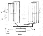
- Fig. 6 is a schematic representation of a sensor array in accordance with another embodiment of the present invention.
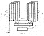
- Fig. 7 is a schematic representation of a sensor array in accordance with a further embodiment of the present invention.
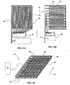
- Figs. 8A to 8C are schematic representations of sensor arrays in accordance with yet another embodiment of the present invention.
- Fig. 9 is a schematic representation of an electronic device incorporating the display device in accordance with one embodiment of the present invention.
- the present invention overcomes the drawback of the prior art electromagnetic digitizers by providing a novel structure for the sensor segments in the sensor array.
- the sensor segment structure may be advantageously adapted for integration into the display module of a display device.
- the present invention will be described in connection with a flat panel display device having an LCD module as the display module, which relies on LC elements as the display elements that can be controlled to render an image.
- the electromagnetic digitizer of the present invention may be incorporated in other types of display devices, flat panel or otherwise, having display modules comprising other types of display elements, such as cathode ray tubes (CRT), organic light emitting diode light emitting elements (OLED), field emission display (FED) elements plasma light emitting elements, fluorescence light emitting elements, chemiluminescent light emitting elements, and other types of light emitting elements.
- CTR cathode ray tubes
- OLED organic light emitting diode light emitting elements
- FED field emission display
- plasma light emitting elements plasma light emitting elements
- fluorescence light emitting elements fluorescence light emitting elements
- chemiluminescent light emitting elements chemiluminescent light emitting elements
- Fig. 2 illustrates a flat panel type display device 10 in accordance with one embodiment of the present invention, which includes an LCD module 12, and a backlight module 14 optically coupled to the LCD module 12.
- the LCD module 12 includes an LC layer 16, supported between two substrates 20 and 22, which can be controlled to regulate and/or filter light transmission to render a composite image based on pixilated image elements. Additional components have been omitted from Fig. 2, to simplify the structure for purpose of disclosing the inventive concept.
- the backlight module 14 may comprise a light source (not shown) that is positioned at an edge or at a planar side. In operation of the LCD module 10, light from the backlight module 14 is regulated, modulated and/or filtered by the LC layer, to render an image in accordance with an image data.
- a controller 26 controls the operation of the LCD module 10 (i.e., effecting control of the LC layer 16 via electrodes and drivers (not shown)).
- the controller 26 may be a part of the display device 10, and/or a part of a computing device to which the display device 10 is operatively attached.
- an electromagnetic digitizer 18 having the novel sensor segment structure of the present invention is supported between the LC layer 16 and the substrate 20, which is operatively coupled to the controller 26.
- the digitizer 18 may be positioned at other locations within the LCD module 12, for example between the LC layer 16 and the substrate 22, or at another intermediate layer location between the substrates 20 and 22 of the LCD module 12.
- the digitizer 18 is integrated into the layers of the LCD module 12 of the display device 10, as opposed to the prior art display devices in which the digitizer panel is provided as a separate component outside the display module (e.g., outside the substrates of the LCD module as shown in Fig. 1). The overall size of the display device 10 is therefore reduced.
- a stylus 24 (e.g., in the shape of a pen) is provided.
- the stylus 24 is operatively coupled to the controller 26, either wirelessly or by a wire.
- the stylus 24 may include one or more button switches, which may be used to select certain input related modes or functions when pressed by a user (e.g., handwriting recognition mode, point and click mode, etc.)
- the stylus includes a magnetic element, which may be a permanent magnet or an electromagnet. As the stylus is moved across the substrate 20, its relative positional coordinates can be determined by the controller 26, based on a change in magnetic flux detected by the sensor segments within the electromagnetic digitizer.
- the basic operational principles of electromagnetic digitizers are well known in the art, and such would not be necessary to be disclosed here.
- the controller 26 controls and synchronizes the operations of the display module 12 including the digitizer, and the stylus. Images are controlled to be displayed by the display module 12, which may require user input by using the stylus to interact with the displayed image (e.g., making a selection by tapping on the display module, drawing or handwriting input by moving the stylus on the display module).
- U.S. Patent Application Serial No. 11/311,986, filed December 20, 2005 which has been commonly assigned to the assignee of the present invention, for further disclosure of the implementation of an electromagnetic digitizer within a display module such as an LCD module, and the control thereof. Further, reference is also made to concurrently filed U.S. Patent Application No. (Attorney Docket No. 1131/216), directed to a process of integrating an electromagnetic digitizer within a display module, such as an LCD module.
- the sensor segment of the electromagnetic digitizer 18 comprises a generally longitudinal structure that includes a network of conductive lines, traces or wires.
- Fig. 3 illustrates the general structure of one embodiment of a sensor segment 30, in accordance with one embodiment of the present invention.
- the sensor segment 30 includes a network of a plurality of parallel conductive lines 32.
- the number of parallel lines depends on the signal sensitivity desired and the overall width of the sensor segment 30, which may vary between two to two hundred lines.
- the width of each trace 32 may range on the order of about 500nm to 500 micrometers.
- the spacing between the lines 32 may range on the order of about 10 micrometers to 20 micrometers.
- the thickness of the lines 32 may range on the order of about 50 nm to 10 micrometers.
- the appropriate dimensions of the conductive lines 32 may be selected depending on factors such as the size of the display area of the display module 12, the desired spatial resolution, pixel density, available areas and locations for placement of the sensor segments within the LCD module 12, etc.
- the overall width of the sensor segment 30 may be wide enough to correspond to the distance across several display pixels (e.g., the traces 32 are spaced apart to cover a distance corresponding to several display pixels).
- FIG. 3 illustrates the spacing to be similar for each pair of adjacent lines 32, such spacing may vary between different pairs of adjacent lines 32 (not shown).
- interconnections are provided between adjacent lines, to form an interconnecting network, resembling a somewhat honeycomb-like structures.
- sensor segments 34, 36 and 38 are illustrated, which are essentially the sensor segment 30 in Fig. 3, provided with interconnections 40 at one or more locations along the generally longitudinal sensor segment structure.
- the interconnections 40 may be in the form of short lines, oriented at an angle between adjacent parallel lines 32. All the interconnections 40 along and between the same pair of adjacent longitudinal lines 32 may be at the same angle and/or orientation (as shown in Figs.
- All the interconnections 40 for all the pairs of adjacent lines 32 may be at the same angle and/or orientation, as in the embodiments of Figs. 4A and 4B, or some of the pairs of adjacent lines 40 may have interconnections 40 at different or mixed angles and/or orientations.
- the angle that an interconnection 40 makes with respect to a trace 32 is preferably not perpendicular (e.g., greater than 0 degree, and less than 90 degrees, and is preferred to be small), to provide a longer interconnection for a particular spacing between a pair of adjacent lines 32.
- the electromagnetic sensitivity of the sensor segments is increased with an increase in available length of the lines within the network in the sensor segment.
- the sensor segments are miniaturized, so that they can be integrated into the display module using semiconductor fabrication processes (i.e., formed into one or more layers within the display module (e.g., between the display element 16 and substrate 20 or substrate 22), as opposed to attached to the outside of the display module as practiced in the prior art).
- semiconductor fabrication processes i.e., formed into one or more layers within the display module (e.g., between the display element 16 and substrate 20 or substrate 22), as opposed to attached to the outside of the display module as practiced in the prior art.
- the details of the steps in these processes have been omitted, as they may involve conventional patterning and photolithographic steps well known in semiconductor processing, such as masking, exposure, doping, deposition, etching, etc., to form structures having desired patterns and conductive properties (including the digitizer sensor arrays).
- the sensitivity of the sensor array can be maintained at a desired level even with significantly smaller overall dimension of the sensor segments. Accordingly, a display module can effectively be provided with integrated sensor arrays, thereby
- the miniaturized sensor segments facilitates integration of electromagnetic digitizers within display modules such as LCD modules, in accordance with the inventive concept disclosed in copending U.S. Patent Application Serial No. 11/311,986, filed December 20, 2005 , which has been commonly assigned to the assignee of the present invention.
- the process of integrating electromagnetic digitizers within display modules such as LCD modules may be referenced to concurrently filed U.S. Patent Application No. (Attorney Docket No. 1131/216), directed to a process of integrating an electromagnetic digitizer within a display module, such as an LCD module.
- Fig. 5A illustrates the embodiment of a sensor array 46, which comprises longitudinal sensor segments 50 arranged in a parallel array.
- the sensor segments 50 include sensor segments that have a generally longitudinal structure that includes a network of conductive lines, traces or wires, disclosed above in accordance with the present invention.
- the sensor segments 50 may have one or more of the structures of sensor segments 30, 34, 36 and 38 shown in Figs. 3, 4A, 4B and 4C, respectively. The number of sensor segments 50 would depend on the resolution and/or sensitivity desired to be achieved.
- the sensor segments 50 comprise eight segments A1 to A8, arranged in a parallel array.
- the segments A1 to A8 may have the same sensor segment structure or different sensor segment structures.
- segments A1 to A8 may each have a structure similar to the sensor segment 34 disclosed in Fig. 4A, or segments A1, A3, A5, A7 and A2, A4, A6, A8 may alternate between the structures of the sensor segments 34 (Fig. 4A) and 36 (Fig. 4B), etc.
- the choice of the particular sensor segment structure would depend on the sensitivity desired to be achieved.
- the overall width of each sensor segment 50 may be wide enough to correspond to the distance across several pixels.
- the parallel sensor segments 50 are operatively coupled to a controller or processor 48.
- One end of each sensor segment 50 is connected in common to ground and/or a terminal of the processor 48.
- Another end of each segment 50 is connected to another set of terminals of a processor 48.
- the processor 48 "scans" each sensor segment 50 in sequence to determine which sensor segment has experienced a change in current caused by a change in magnetic induction in the presence of the stylus 24.
- Fig. 5A represents an X-array, allowing determination of the X-position of the stylus 24 across the sensor array 46.
- Fig. 5B represents a sensor array 54, which functions as a Y-array, allowing determination of the Y-position of the stylus 24.
- the sensor array 54 may be similar in structure to the sensor array 46 in Fig. 5B.
- the sensor array 54 comprises longitudinal sensor segments 52 arranged in a parallel array.
- the sensor segments 52 include sensor segments that have a generally longitudinal structure that includes a network of conductive lines, traces or wires, disclosed above in accordance with the present invention.
- the sensor segments 52 may have one or more of the structures of sensor segments 30, 34, 36 and 38 shown in Figs. 3, 4A, 4B and 4C, respectively.
- the sensor segments 52 comprise eight segments B1 to B10, arranged in a parallel array.
- the segments B1 to B10 may have the same sensor segment structure or different sensor segment structures.
- segments B 1 to B10 may each have a structure similar to the sensor segment 34 disclosed in Fig. 4A, or segments B1, B3, B5, B7, B9 and B2, B4, B6, B8, B10 may alternate between the structures of the sensor segments 34 (Fig. 4A) and 36 (Fig. 4B), etc.
- the parallel sensor segments 52 are operatively coupled to a controller or processor 56.
- One end of each sensor segment 52 is connected in common to ground and/or a terminal of the processor 56.
- Another end of each segment 52 is connected to another set of terminals of the processor 56.
- the processor 56 "scans" each sensor segment 52 in sequence to determine which sensor segment has experienced a change in current caused by a change in magnetic induction in the presence of the stylus 24.
- the sensor arrays 46 and 54 are stacked in a spaced apart configuration, in an orthogonal manner, as schematically shown in Fig. 5C, to form the complete electromagnetic digitizer 18, which may be implemented on the inside surface of the top substrate 20, as shown in Fig. 2.
- the two sensor arrays 46 and 54 may be separated by a dielectric material (not shown in the simplified view in Fig. 5C), in a thickness, for example, ranging between 5 to 10000nm.
- the sensor arrays 46 and 54 may be commonly grounded by interconnecting at 58 the grounding ends of the sensor segments in the sensor arrays through a via in the dielectric material (not shown).
- the sensor arrays 46 and 54 are operatively coupled to the controller 26, which includes the X-processor 48 and Y-processor 56. Further, the X-processor 48 and Y-processor 56 may be a single processor having dual functions for controlling X sensor array 46 and Y sensor array 54.
- the X sensor array 46 and the Y sensor array 54 do not need to have sensor segments that each have a network of conductive lines in accordance with the present invention.
- the X sensor array 46 may have sensor segments each having a network of conductive lines in accordance with the present invention, but the Y sensor array 54 may have sensor segments that each has a single wire structure found in the prior art, or vice versa.
- the X sensor array and the Y sensor array may be mixed and matched with different types of sensor segment structures for the respective sensor arrays.
- Fig. 6 schematically illustrates another embodiment of a sensor array 60, which comprises half loop or U-shaped sensor segments 62 arranged in an overlapping parallel array.
- the overlapping U-shaped sensor segments 62 are separated by dielectric layers (not shown), such that that the U-shaped sensor segments 62 are electrically insulated from one another.
- the U-shaped sensor segments 62 include segments that have a generally longitudinal structure that includes a network of conductive lines, traces or wires, disclosed above in accordance with the present invention.
- the U-shaped sensor segments 62 may have one or more of the structures of sensor segments 30, 34, 36 and 38 shown in Figs. 3, 4A, 4B and 4C, respectively.
- the parallel-connected sensor segments 62 are operatively coupled to a controller or processor 64.
- each U-shaped sensor segment 62 is connected in common to ground and/or a terminal of the processor 64. Another end of each U-shaped sensor segment 62 is connected to another set of terminals of the processor 64.
- the processor 64 "scans" each U-shaped sensor segment 62 in sequence to determine which sensor segment has experienced a change in current caused by a change in magnetic induction in the presence of the stylus 24.
- Fig. 6 represents an X-array, allowing determination of the X-position of the stylus 24 across the sensor array 60.
- a Y sensor array (not shown) is provided to allow determination of the Y-position of the stylus 24.
- the Y sensor array may have an array configuration and sensor segments that are similar in structure to those in the sensor array 60 in Fig. 6, but with the longitudinal sensor segments configured orthogonal to the longitudinal segments 62.
- the Y sensor array may take on a configuration similar to the Y sensor 54 in Fig. 5B.
- the Y sensor array may have sensor array and sensor segments that are similar to conventional sensor array and sensor segment.
- the X sensor array 60 and the Y sensor array (not shown) are stacked in a spaced apart configuration, in an orthogonal manner, as in the previous embodiment schematically shown in Fig. 5C, to form a complete electromagnetic digitizer 18.
- the sensor array 70 comprises full loop sensor segments 72 arranged in an overlapping parallel array.
- each full loop sensor segment is not in a closed loop, but in a spiral loop.
- each full loop sensor segment spirals counterclockwise in a direction into the X-Y plane (i.e., in the ⁇ Z direction).
- each full loop sensor segment could spiral clockwise, in a direction into the X-Y plane (i.e., in the ⁇ Z direction).
- the overlapping full loop sensor segments 72 are separated by dielectric layers (not shown), such that the full loop sensor segments 72 are electrically insulated from one another. Further, overlapping sections within a full loop sensor segment are also separated by a dielectric layer.
- the full loop sensor segments 72 include segments that have a generally longitudinal structure that includes a network of conductive lines, traces or wires, disclosed above in accordance with the present invention.
- the full loop sensor segments 72 may have one or more of the structures of sensor segments 30, 34, 36 and 38 shown in Figs. 3, 4A, 4B and 4C, respectively.
- the parallel-connected sensor segments 72 are operatively coupled to a controller or processor 74.
- One end of each full loop sensor segment 72 is connected in common to ground and/or a terminal of the processor 74.
- Another end of each U-shaped sensor segment 72 is connected to another set of terminals of the processor 74.
- the processor 74 "scans" each U-shaped sensor segment 72 in sequence to determine which sensor segment has experienced a change in current caused by a change in magnetic induction in the presence of the stylus 24.
- Fig. 7 represents an X-array, allowing determination of the X-position of the stylus 24 across the sensor array 70.
- a Y sensor array (not shown) is provided to allow determination of the Y-position of the stylus 24.
- the Y sensor array may have an array configuration and sensor segments that are similar in structure to those in the sensor array 70 in Fig. 7, but with the longitudinal sensor segments configured orthogonal to the longitudinal segments 72.
- the Y sensor array may take on a configuration similar to the Y sensor 54 in Fig. 5B, or a configuration similar to the X sensor array 60 in Fig. 6 (but arranged in an orthogonal manner).
- the Y sensor array may have sensor array and sensor segments that are similar to conventional sensor array and sensor segment.
- the X sensor array 60 and the Y sensor array are stacked in a spaced apart configuration, in an orthogonal manner, separated by a dielectric layer, as in the previous embodiment schematically shown in Fig. 5C, to form a complete electromagnetic digitizer 18.
- FIG. 8A shows a sensor array 80 that includes a similar structure as the X sensor array 46 in Fig. 5A, having sensor segments 50, and further additional sensor lines 82 between adjacent sensor segments 52.
- the additional sensor segments 82 may have one or more of the structures of sensor segments 30, 34, 36 and 38 shown in Figs. 3, 4A, 4B and 4C, respectively.
- the additional sensor lines 82 may be at the same voltage potential (e.g., connected to a fixed reference voltage or ground), or electrically isolated or floating.
- An X processor 84 is operatively coupled to the sensor array 80.
- the X sensor array 80 may be used with a Y sensor array that can take a structure similar to the sensor array 54 in Fig. 5B, or the configuration similar to the X sensor array 60 in Fig. 6, or the X sensor array 70 in Fig. 7 (but arranged in an orthogonal manner).
- the Y sensor array may take on a structure similar to the X sensor array 80 in Fig. 8, but arranged in an orthogonal manner, as shown in Fig. 8B.
- the Y sensor array 86 is essentially the sensor array 54 in Fig. 5B, with further additional sensor lines 88 in between adjacent sensor segments 52.
- the additional sensor segments 88 may have one or more of the structures of sensor segments 30, 34, 36 and 38 shown in Figs.
- the additional sensor lines 88 may be at the same voltage potential (e.g., connected to a fixed reference voltage or ground), or electrically isolated or floating.
- the Y sensor array 86 is operatively coupled to a Y processor 89.
- the X sensor array 80 and the Y sensor array 86 are stacked in a spaced apart configuration, in an orthogonal manner, separated by a dielectric layer, as in the previous embodiment schematically shown in Fig. 5C, to form a complete electromagnetic digitizer 18.
- the sensor arrays 80 and 86 may be commonly grounded by interconnecting at 58 the grounding ends of the sensor segments in the sensor arrays through a via in the dielectric material (not shown).
- the sensor arrays 80 and 86 are operatively coupled to the controller 26, which includes the X-processor 84 and Y-processor 89. Further, the X-processor 84 and Y-processor 89 may be a single processor having dual functions for controlling X sensor array 80 and Y sensor array 86.
- the configurations of the sensor arrays shown in Figs. 5, 6, 7 and 8 may be mixed and combined in a single sensor array, without departing from the scope and spirit of the present invention.
- the electromagnetic digitizer by combining different sensor array components over the entire digitizer planar area (e.g., using parallel straight sensor segments at certain area of the digitizer, using parallel half-loop sensor segments in another area of the digitizer, using parallel full looped sensor segments in a further area of the digitizer, and using additional floating conductive lines between adjacent sensor segments in yet another area of the digitizer), different desired sensitivities may be achieved at different areas of the digitizer.
- the sensitivity at certain areas of the display may not be required to be as high as the sensitivity at another area of the display (e.g., the area designated for hand writing recognition).
- Fig. 9 schematically shows an embodiment of an electronic device 100, which includes a display system 102 for displaying images, and an input/output (I/O) controller 103 for providing image data to the display system 102 and instructing the display system 102 to render an image in accordance with the image data.
- the display system 102 includes the display device 10 (e.g., an LCD device) in accordance with the present invention and an interface controller 106 exchanging image data and user input data (from the digitizer 18) with the I/O controller 103.
- the display device incorporates a display module (e.g., an LCD module) having an integrated electromagnetic digitizer 18 of the present invention and a controller 26 (e.g., drivers).
- the electronic device 100 may include a laptop computer, a mobile phone, a digital camera, a personal digital assistant (PDA), a desktop computer, a television, a car display or a portable DVD player.
- PDA personal digital assistant
Landscapes
- Engineering & Computer Science (AREA)
- General Engineering & Computer Science (AREA)
- Theoretical Computer Science (AREA)
- Physics & Mathematics (AREA)
- Human Computer Interaction (AREA)
- General Physics & Mathematics (AREA)
- Electromagnetism (AREA)
- Position Input By Displaying (AREA)
- Devices For Indicating Variable Information By Combining Individual Elements (AREA)
- Measurement Of Length, Angles, Or The Like Using Electric Or Magnetic Means (AREA)
Applications Claiming Priority (2)
| Application Number | Priority Date | Filing Date | Title |
|---|---|---|---|
| US70116005P | 2005-07-21 | 2005-07-21 | |
| US70129705P | 2005-07-21 | 2005-07-21 |
Publications (1)
| Publication Number | Publication Date |
|---|---|
| EP1746488A2 true EP1746488A2 (de) | 2007-01-24 |
Family
ID=37036825
Family Applications (1)
| Application Number | Title | Priority Date | Filing Date |
|---|---|---|---|
| EP06117603A Withdrawn EP1746488A2 (de) | 2005-07-21 | 2006-07-20 | Sensoranordnungsstruktur eines elektromagnetischen Digitalisierers |
Country Status (4)
| Country | Link |
|---|---|
| US (1) | US7875814B2 (de) |
| EP (1) | EP1746488A2 (de) |
| KR (1) | KR101333213B1 (de) |
| TW (2) | TWI349216B (de) |
Cited By (5)
| Publication number | Priority date | Publication date | Assignee | Title |
|---|---|---|---|---|
| WO2009154812A2 (en) | 2008-02-28 | 2009-12-23 | 3M Innovative Properties Company | Touch screen sensor |
| EP2260367A4 (de) * | 2008-02-28 | 2014-05-14 | 3M Innovative Properties Co | Berührungsschirmsensor mit leitern geringer sichtbarkeit |
| EP2260366A4 (de) * | 2008-02-28 | 2014-10-08 | 3M Innovative Properties Co | Berührungsschirmsensor mit veränderlichem flächenwiderstand |
| EP2811370A3 (de) * | 2013-05-08 | 2015-02-18 | Tianma Micro-Electronics Co. Ltd | Induktiver Berührungsbildschirm und induktiver Berührungsbildschirm in einer Zelle |
| EP3196742A1 (de) * | 2016-01-19 | 2017-07-26 | Samsung Display Co., Ltd. | Messvorrichtung mit elektronischem stift und anzeigevorrichtung |
Families Citing this family (304)
| Publication number | Priority date | Publication date | Assignee | Title |
|---|---|---|---|---|
| US7821425B2 (en) | 2002-07-12 | 2010-10-26 | Atmel Corporation | Capacitive keyboard with non-locking reduced keying ambiguity |
| GB2418493B (en) | 2003-08-21 | 2006-11-15 | Harald Philipp | Capacitive position sensor |
| GB0319714D0 (en) | 2003-08-21 | 2003-09-24 | Philipp Harald | Anisotropic touch screen element |
| GB2428306B (en) | 2005-07-08 | 2007-09-26 | Harald Philipp | Two-dimensional capacitive position sensor |
| US7932898B2 (en) | 2005-09-20 | 2011-04-26 | Atmel Corporation | Touch sensitive screen |
| GB2437827B (en) * | 2006-05-05 | 2008-03-26 | Harald Philipp | Touch screen element |
| US7903092B2 (en) * | 2006-05-25 | 2011-03-08 | Atmel Corporation | Capacitive keyboard with position dependent reduced keying ambiguity |
| US8619054B2 (en) | 2006-05-31 | 2013-12-31 | Atmel Corporation | Two dimensional position sensor |
| US8786554B2 (en) * | 2006-07-10 | 2014-07-22 | Atmel Corporation | Priority and combination suppression techniques (PST/CST) for a capacitive keyboard |
| US7830160B2 (en) * | 2006-10-20 | 2010-11-09 | Atmel, Corporation | Capacitive position sensor |
| US20080094077A1 (en) * | 2006-10-20 | 2008-04-24 | Harald Philipp | Capacitive Position Sensor |
| GB2446702A (en) * | 2007-02-13 | 2008-08-20 | Qrg Ltd | Touch Control Panel with Pressure Sensor |
| TWI444876B (zh) * | 2007-04-05 | 2014-07-11 | Qrg Ltd | 二維位置感應器 |
| KR101526626B1 (ko) * | 2007-07-12 | 2015-06-05 | 아트멜 코포레이션 | 2차원 터치 패널 |
| GB2451267A (en) * | 2007-07-26 | 2009-01-28 | Harald Philipp | Capacitive position sensor |
| US7952366B2 (en) | 2007-07-26 | 2011-05-31 | Atmel Corporation | Proximity sensor |
| TW200915162A (en) * | 2007-07-31 | 2009-04-01 | Qrg Ltd | Sensor and method of sensing |
| US8536880B2 (en) * | 2007-08-26 | 2013-09-17 | Atmel Corporation | Capacitive sensor with additional noise-registering electrode |
| JP2011517367A (ja) * | 2008-02-28 | 2011-06-02 | スリーエム イノベイティブ プロパティズ カンパニー | 基材上に導電体をパターン化する方法 |
| US8284332B2 (en) * | 2008-08-01 | 2012-10-09 | 3M Innovative Properties Company | Touch screen sensor with low visibility conductors |
| US8830201B2 (en) | 2008-03-25 | 2014-09-09 | Elan Microelectronics Corporation | Equalized capacitive touchpad and touch positioning method |
| TW200941320A (en) * | 2008-03-25 | 2009-10-01 | Elan Microelectronics Corp | Equalized capacitive touchpad and touch positioning method |
| TW201008118A (en) | 2008-04-10 | 2010-02-16 | Atmel Corp | Capacitive touch screen with noise suppression |
| US8526767B2 (en) * | 2008-05-01 | 2013-09-03 | Atmel Corporation | Gesture recognition |
| US9569037B2 (en) * | 2008-05-19 | 2017-02-14 | Atmel Corporation | Capacitive sensing with low-frequency noise reduction |
| US9069418B2 (en) * | 2008-06-06 | 2015-06-30 | Apple Inc. | High resistivity metal fan out |
| TWI367440B (en) * | 2008-06-26 | 2012-07-01 | Qisda Corp | Touch panel with touch keys |
| US8482545B2 (en) | 2008-10-02 | 2013-07-09 | Wacom Co., Ltd. | Combination touch and transducer input system and method |
| CN102171928A (zh) * | 2008-10-04 | 2011-08-31 | 爱特梅尔公司 | 电容性矩阵触摸传感器 |
| US8638314B2 (en) * | 2008-10-17 | 2014-01-28 | Atmel Corporation | Capacitive touch buttons combined with electroluminescent lighting |
| US20100097329A1 (en) * | 2008-10-21 | 2010-04-22 | Martin Simmons | Touch Position Finding Method and Apparatus |
| US8056044B2 (en) | 2008-10-21 | 2011-11-08 | Atmel Corporation | Signal processing |
| US8866790B2 (en) * | 2008-10-21 | 2014-10-21 | Atmel Corporation | Multi-touch tracking |
| US8659557B2 (en) * | 2008-10-21 | 2014-02-25 | Atmel Corporation | Touch finding method and apparatus |
| US8605037B2 (en) * | 2008-10-21 | 2013-12-10 | Atmel Corporation | Noise reduction in capacitive touch sensors |
| US8054090B2 (en) | 2008-10-22 | 2011-11-08 | Atmel Corporation | Noise handling in capacitive touch sensors |
| US8610009B2 (en) * | 2008-10-22 | 2013-12-17 | Atmel Corporation | Capacitive touch sensors |
| US8552995B2 (en) * | 2008-10-22 | 2013-10-08 | Atmel Corporation | Sensor and method of sensing |
| KR101033997B1 (ko) * | 2008-11-11 | 2011-05-11 | 주식회사 애트랩 | 터치 패널 및 이를 구비하는 입력 장치 |
| US9244568B2 (en) * | 2008-11-15 | 2016-01-26 | Atmel Corporation | Touch screen sensor |
| WO2010075308A2 (en) | 2008-12-26 | 2010-07-01 | Atmel Corporation | Multiple electrode touch sensitive device |
| CN102334091B (zh) * | 2009-02-26 | 2016-01-06 | 3M创新有限公司 | 触摸屏传感器和具有低可见度的覆盖微图案的图案化基材 |
| US8237456B2 (en) | 2009-03-02 | 2012-08-07 | Atmel Corporation | Capacitive sensing |
| US9495042B2 (en) * | 2009-04-14 | 2016-11-15 | Atmel Corporation | Two-dimensional position sensor |
| US8810523B2 (en) * | 2009-04-20 | 2014-08-19 | Broadcom Corporation | Inductive touch screen and methods for use therewith |
| US8154529B2 (en) | 2009-05-14 | 2012-04-10 | Atmel Corporation | Two-dimensional touch sensors |
| US8253706B2 (en) | 2009-06-26 | 2012-08-28 | Atmel Corporation | Apparatus using a differential analog-to-digital converter |
| US8451237B2 (en) * | 2009-07-06 | 2013-05-28 | Atmel Corporation | Sensitivity control as a function of touch shape |
| US20110007011A1 (en) * | 2009-07-13 | 2011-01-13 | Ocular Lcd Inc. | Capacitive touch screen with a mesh electrode |
| TWI395129B (zh) * | 2009-07-28 | 2013-05-01 | Hanwang Technology Co Ltd | An electromagnetic induction scrolling information input method and device |
| US8490013B2 (en) | 2009-07-30 | 2013-07-16 | Atmel Corporation | Method and apparatus for single touch zoom using spiral rotation |
| US20130009907A1 (en) * | 2009-07-31 | 2013-01-10 | Rosenberg Ilya D | Magnetic Stylus |
| US8621942B2 (en) * | 2009-08-03 | 2014-01-07 | Atmel Corporation | Force sensor with compressible electrode |
| US9836167B2 (en) * | 2009-08-03 | 2017-12-05 | Atmel Corporation | Electrode layout for touch screens |
| US8279189B2 (en) | 2009-08-11 | 2012-10-02 | Atmel Corporation | Touch-sensitive user interface |
| US8576182B2 (en) * | 2009-09-01 | 2013-11-05 | Atmel Corporation | Methods and apparatuses to test the functionality of capacitive sensors |
| US8552315B2 (en) * | 2009-09-03 | 2013-10-08 | Atmel Corporation | Two-dimensional position sensor |
| US8730199B2 (en) | 2009-09-04 | 2014-05-20 | Atmel Corporation | Capacitive control panel |
| US8552994B2 (en) * | 2009-09-25 | 2013-10-08 | Atmel Corporation | Method and apparatus to measure self-capacitance using a single pin |
| US8797290B2 (en) * | 2009-10-22 | 2014-08-05 | Atmel Corporation | Sense electrode spine interpolation |
| US9041682B2 (en) * | 2009-10-23 | 2015-05-26 | Atmel Corporation | Driving electrodes with different phase signals |
| US9632628B2 (en) * | 2009-10-23 | 2017-04-25 | Atmel Corporation | Interdigitated touchscreen electrodes |
| US8564552B2 (en) * | 2009-10-26 | 2013-10-22 | Atmel Corporation | Touchscreen electrode arrangement with varied proportionate density |
| US9916045B2 (en) | 2009-10-26 | 2018-03-13 | Amtel Corporation | Sense electrode design |
| US9372579B2 (en) | 2009-10-27 | 2016-06-21 | Atmel Corporation | Touchscreen electrode arrangement |
| US20110102331A1 (en) * | 2009-10-29 | 2011-05-05 | Qrg Limited | Redundant touchscreen electrodes |
| US8599150B2 (en) * | 2009-10-29 | 2013-12-03 | Atmel Corporation | Touchscreen electrode configuration |
| US9489072B2 (en) | 2010-04-15 | 2016-11-08 | Atmel Corporation | Noise reduction in capacitive touch sensors |
| US8860686B2 (en) | 2010-04-30 | 2014-10-14 | Atmel Corporation | Multi-chip touch screens |
| US8766929B2 (en) | 2010-05-14 | 2014-07-01 | Atmel Corporation | Panel for position sensors |
| US8797280B2 (en) | 2010-05-26 | 2014-08-05 | Atmel Corporation | Systems and methods for improved touch screen response |
| WO2011156447A1 (en) * | 2010-06-11 | 2011-12-15 | 3M Innovative Properties Company | Positional touch sensor with force measurement |
| US8797281B2 (en) | 2010-06-16 | 2014-08-05 | Atmel Corporation | Touch-screen panel with multiple sense units and related methods |
| US10306758B2 (en) | 2010-07-16 | 2019-05-28 | Atmel Corporation | Enhanced conductors |
| US9081427B2 (en) | 2010-07-16 | 2015-07-14 | Atmel Corporation | Position-sensing panel and method |
| US8723834B2 (en) | 2010-07-28 | 2014-05-13 | Atmel Corporation | Touch sensitive screen configurations |
| US10831317B2 (en) | 2010-08-20 | 2020-11-10 | Neodrón Limited | Electronic ink touch sensitive display |
| US8823656B2 (en) | 2010-08-30 | 2014-09-02 | Atmel Corporation | Touch tracking across multiple touch screens |
| US8723818B2 (en) | 2010-09-10 | 2014-05-13 | Atmel Corporation | Touch screen poly layer electrode distribution |
| US9252768B2 (en) | 2010-09-13 | 2016-02-02 | Atmel Corporation | Position-sensing panel |
| TWI423194B (zh) * | 2010-09-21 | 2014-01-11 | Waltop Int Corp | 整合電磁式感應輸入之平面顯示裝置與薄膜電晶體陣列基板 |
| US9626045B1 (en) | 2010-09-27 | 2017-04-18 | Atmel Corporation | Position-sensing panel and related methods |
| US8400209B2 (en) | 2010-10-22 | 2013-03-19 | Atmel Corporation | Proximity detection |
| US8564314B2 (en) | 2010-11-02 | 2013-10-22 | Atmel Corporation | Capacitive touch sensor for identifying a fingerprint |
| US8786572B2 (en) | 2010-11-04 | 2014-07-22 | Atmel Corporation | Touch position-sensing panel and method |
| US9223445B2 (en) | 2010-12-02 | 2015-12-29 | Atmel Corporation | Position-sensing and force detection panel |
| US9077344B2 (en) | 2010-12-07 | 2015-07-07 | Atmel Corporation | Substrate for electrical component and method |
| US8866491B2 (en) | 2011-02-24 | 2014-10-21 | Cypress Semiconductor Corporation | Tail effect correction for SLIM pattern touch panels |
| US9952737B2 (en) * | 2011-02-24 | 2018-04-24 | Parade Technologies, Ltd. | Single layer touch sensor |
| US8947404B2 (en) | 2011-03-09 | 2015-02-03 | Atmel Corporation | Stylus |
| US9007332B2 (en) | 2011-03-22 | 2015-04-14 | Atmel Corporation | Position sensing panel |
| US8797285B2 (en) | 2011-04-18 | 2014-08-05 | Atmel Corporation | Panel |
| US9218561B2 (en) | 2011-05-25 | 2015-12-22 | Atmel Corporation | Touch sensor with RFID |
| US8624607B2 (en) | 2011-07-29 | 2014-01-07 | Atmel Corporation | Measuring voltage |
| US9501179B2 (en) | 2011-08-04 | 2016-11-22 | Atmel Corporation | Touch sensor for curved or flexible surfaces |
| US9287865B2 (en) | 2011-08-10 | 2016-03-15 | Atmel Corporation | Capacitive touch sensor control unit with sampling capacitors for differential integration |
| US10044353B2 (en) | 2011-08-10 | 2018-08-07 | Atmel Corporation | Substantially edgeless touch sensor |
| US8421666B2 (en) | 2011-08-11 | 2013-04-16 | Atmel Corporation | Analog to digital converter with adjustable conversion window |
| US8416117B2 (en) | 2011-08-11 | 2013-04-09 | Atmel Corporation | Analog to digital converter with dual integrating capacitor systems |
| US10222912B2 (en) | 2011-09-06 | 2019-03-05 | Atmel Corporation | Touch sensor with touch object discrimination |
| US8847898B2 (en) | 2011-09-07 | 2014-09-30 | Atmel Corporation | Signal-to-noise ratio in touch sensors |
| US8847612B2 (en) | 2011-09-08 | 2014-09-30 | Atmel Corporation | Integrated test system for a touch sensor |
| US9195351B1 (en) | 2011-09-28 | 2015-11-24 | Amazon Technologies, Inc. | Capacitive stylus |
| US9310941B2 (en) | 2011-10-04 | 2016-04-12 | Atmel Corporation | Touch sensor input tool with offset between touch icon and input icon |
| US9256311B2 (en) | 2011-10-28 | 2016-02-09 | Atmel Corporation | Flexible touch sensor |
| US8947379B2 (en) | 2011-10-28 | 2015-02-03 | Atmel Corporation | Inductive charging for active stylus |
| US9389701B2 (en) | 2011-10-28 | 2016-07-12 | Atmel Corporation | Data transfer from active stylus |
| US9250719B2 (en) | 2011-10-28 | 2016-02-02 | Atmel Corporation | Active stylus with filter |
| US8933899B2 (en) | 2011-10-28 | 2015-01-13 | Atmel Corporation | Pulse- or frame-based communication using active stylus |
| US8797287B2 (en) | 2011-10-28 | 2014-08-05 | Atmel Corporation | Selective scan of touch-sensitive area for passive or active touch or proximity input |
| US9116558B2 (en) | 2011-10-28 | 2015-08-25 | Atmel Corporation | Executing gestures with active stylus |
| US9389707B2 (en) | 2011-10-28 | 2016-07-12 | Atmel Corporation | Active stylus with configurable touch sensor |
| US9354728B2 (en) | 2011-10-28 | 2016-05-31 | Atmel Corporation | Active stylus with capacitive buttons and sliders |
| US9086745B2 (en) | 2011-10-28 | 2015-07-21 | Atmel Corporation | Dynamic reconfiguration of electrodes in an active stylus |
| US8872792B2 (en) | 2011-10-28 | 2014-10-28 | Atmel Corporation | Active stylus with energy harvesting |
| US8581886B2 (en) | 2011-10-28 | 2013-11-12 | Atmel Corporation | Tuning algorithm for noise reduction in an active stylus |
| US9189121B2 (en) | 2011-10-28 | 2015-11-17 | Atmel Corporation | Active stylus with filter having a threshold |
| US10162400B2 (en) | 2011-10-28 | 2018-12-25 | Wacom Co., Ltd. | Power management system for active stylus |
| US9182856B2 (en) | 2011-10-28 | 2015-11-10 | Atmel Corporation | Capacitive force sensor |
| US9459709B2 (en) | 2011-10-28 | 2016-10-04 | Atmel Corporation | Scaling voltage for data communication between active stylus and touch-sensor device |
| US10423248B2 (en) | 2011-10-28 | 2019-09-24 | Wacom Co., Ltd. | Touch-sensitive system with motion filtering |
| US9946408B2 (en) | 2011-10-28 | 2018-04-17 | Atmel Corporation | Communication between a master active stylus and a slave touch-sensor device |
| US9874920B2 (en) | 2011-10-28 | 2018-01-23 | Atmel Corporation | Power management system for active stylus |
| US9280218B2 (en) | 2011-10-28 | 2016-03-08 | Atmel Corporation | Modulating drive signal for communication between active stylus and touch-sensor device |
| US10082889B2 (en) | 2011-10-28 | 2018-09-25 | Atmel Corporation | Multi-electrode active stylus tip |
| US9164603B2 (en) | 2011-10-28 | 2015-10-20 | Atmel Corporation | Executing gestures with active stylus |
| US10725563B2 (en) | 2011-10-28 | 2020-07-28 | Wacom Co., Ltd. | Data transfer from active stylus to configure a device or application |
| US9160331B2 (en) | 2011-10-28 | 2015-10-13 | Atmel Corporation | Capacitive and inductive sensing |
| US9164598B2 (en) | 2011-10-28 | 2015-10-20 | Atmel Corporation | Active stylus with surface-modification materials |
| US11347330B2 (en) | 2011-10-28 | 2022-05-31 | Wacom Co., Ltd. | Adaptive transmit voltage in active stylus |
| US10725564B2 (en) | 2011-10-28 | 2020-07-28 | Wacom Co., Ltd. | Differential sensing in an active stylus |
| US9606641B2 (en) | 2015-03-09 | 2017-03-28 | Atmel Corporation | Adaptive transmit voltage in active stylus |
| US9557833B2 (en) | 2011-10-28 | 2017-01-31 | Atmel Corporation | Dynamic adjustment of received signal threshold in an active stylus |
| US8866767B2 (en) | 2011-10-28 | 2014-10-21 | Atmel Corporation | Active stylus with high voltage |
| US9965107B2 (en) | 2011-10-28 | 2018-05-08 | Atmel Corporation | Authenticating with active stylus |
| US9690431B2 (en) | 2011-10-28 | 2017-06-27 | Atmel Corporation | Locking active stylus and touch-sensor device |
| US8963561B2 (en) | 2011-11-03 | 2015-02-24 | Atmel Corporation | Randomizing one or more micro-features of a touch sensor |
| US9337833B2 (en) | 2011-11-14 | 2016-05-10 | Atmel Corporation | Driven shield for shaping an electric field of a touch sensor |
| US9825104B2 (en) | 2011-11-22 | 2017-11-21 | Atmel Corporation | Low-birefringence substrate for touch sensor |
| US9317161B2 (en) | 2011-11-22 | 2016-04-19 | Atmel Corporation | Touch sensor with spacers supporting a cover panel |
| US9965106B2 (en) | 2011-11-22 | 2018-05-08 | Atmel Corporation | Touch screen with electrodes positioned between pixels |
| US8711292B2 (en) | 2011-11-22 | 2014-04-29 | Atmel Corporation | Integrated touch screen |
| US9262019B2 (en) | 2011-11-22 | 2016-02-16 | Atmel Corporation | Touch sensor with conductive lines having different widths |
| US8947105B2 (en) | 2011-12-01 | 2015-02-03 | Atmel Corporation | Capacitive coupling of bond pads |
| US9024645B2 (en) | 2011-12-06 | 2015-05-05 | Atmel Corporation | Substantially edgeless touch sensor |
| US9507447B2 (en) | 2011-12-08 | 2016-11-29 | Atmel Corporation | Touch sensor with inductive charging |
| US9411472B2 (en) | 2011-12-08 | 2016-08-09 | Atmel Corporation | Touch sensor with adaptive touch detection thresholding |
| US9207814B2 (en) | 2011-12-14 | 2015-12-08 | Atmel Corporation | Single-layer touch sensor |
| US8860690B2 (en) | 2011-12-15 | 2014-10-14 | Atmel Corporation | Touch sensor with capacitive nodes having a capacitance that is approximately the same |
| US9634660B2 (en) | 2011-12-20 | 2017-04-25 | Atmel Corporation | Touch sensor with reduced anti-touch effects |
| US9372580B2 (en) | 2011-12-21 | 2016-06-21 | Atmel Corporation | Enhanced touch detection methods |
| US9312855B2 (en) | 2012-01-10 | 2016-04-12 | Atmel Corporation | Touch sensor tracks |
| US9071249B2 (en) | 2012-01-11 | 2015-06-30 | Atmel Corporation | Corrosion resistant touch sensor |
| US9244570B2 (en) | 2012-01-17 | 2016-01-26 | Atmel Corporation | System and method for reducing the effects of parasitic capacitances |
| US20130181911A1 (en) | 2012-01-17 | 2013-07-18 | Esat Yilmaz | On-Display-Sensor Stack |
| US8890824B2 (en) | 2012-02-07 | 2014-11-18 | Atmel Corporation | Connecting conductive layers using in-mould lamination and decoration |
| US9160332B2 (en) | 2012-02-07 | 2015-10-13 | Atmel Corporation | Method and system for mechanical coupling of flexible printed circuit to a sensor |
| US9471185B2 (en) | 2012-02-21 | 2016-10-18 | Atmel Corporation | Flexible touch sensor input device |
| US9154127B2 (en) | 2012-03-06 | 2015-10-06 | Atmel Corporation | Touch sensor with conductive lines having portions with different widths |
| US9069423B2 (en) | 2012-03-07 | 2015-06-30 | Atmel Corporation | Buffer-reference self-capacitance measurement |
| KR20130107886A (ko) * | 2012-03-23 | 2013-10-02 | 삼성전기주식회사 | 디지타이저 |
| FR2988872B1 (fr) * | 2012-03-29 | 2014-03-28 | Commissariat Energie Atomique | Ecran avec localisation d'objet magnetique |
| US8896327B2 (en) | 2012-04-12 | 2014-11-25 | Atmel Corporation | Current mirror self-capacitance measurement |
| US9372582B2 (en) | 2012-04-19 | 2016-06-21 | Atmel Corporation | Self-capacitance measurement |
| US9306560B2 (en) | 2012-05-14 | 2016-04-05 | Atmel Corporation | Self-capacitance detection using trans-conductance reference |
| US8952927B2 (en) | 2012-05-18 | 2015-02-10 | Atmel Corporation | Self-capacitance measurement with compensated capacitance |
| US9013444B2 (en) | 2012-05-18 | 2015-04-21 | Atmel Corporation | Self-capacitance measurement with isolated capacitance |
| US9921691B2 (en) | 2012-05-18 | 2018-03-20 | Atmel Corporation | Burst-mode self-capacitance measurement with compensated capacitance |
| US9459737B2 (en) | 2012-05-23 | 2016-10-04 | Atmel Corporation | Proximity detection using multiple inputs |
| US9046942B2 (en) | 2012-06-01 | 2015-06-02 | Atmel Corporation | Combined accumulator and maximum/minimum comparator |
| US8917261B2 (en) | 2012-06-26 | 2014-12-23 | Atmel Corporation | Pixel occlusion mitigation |
| US8941014B2 (en) | 2012-06-28 | 2015-01-27 | Atmel Corporation | Complex adhesive boundaries for touch sensors |
| US8803004B2 (en) | 2012-06-28 | 2014-08-12 | Atmel Corporation | Complex adhesive boundaries for touch sensors |
| US9262023B2 (en) | 2012-07-09 | 2016-02-16 | Atmel Corporation | Drive signals for a touch sensor |
| JP5224203B1 (ja) | 2012-07-11 | 2013-07-03 | 大日本印刷株式会社 | タッチパネルセンサ、タッチパネル装置および表示装置 |
| US8736551B2 (en) | 2012-07-12 | 2014-05-27 | Atmel Corporation | Touch-sensor-controller sensor hub |
| US9098152B2 (en) | 2012-07-24 | 2015-08-04 | Atmel Corporation | Dielectric layer for touch sensor stack |
| US9116584B2 (en) | 2012-07-24 | 2015-08-25 | Atmel Corporation | Dielectric layer for touch sensor stack |
| KR20140018017A (ko) * | 2012-08-03 | 2014-02-12 | 삼성전기주식회사 | 디지타이저 |
| US9354737B2 (en) | 2012-08-09 | 2016-05-31 | Atmel Corporation | Active stylus self-capacitance measurement |
| US9563304B2 (en) | 2012-08-15 | 2017-02-07 | Atmel Corporation | Active stylus with passive mutual measurements |
| KR20140024741A (ko) * | 2012-08-21 | 2014-03-03 | 삼성전기주식회사 | 디지타이저 |
| US8502796B1 (en) | 2012-08-27 | 2013-08-06 | Atmel Corporation | Interpolated single-layer touch sensor |
| US9035663B2 (en) | 2012-09-11 | 2015-05-19 | Atmel Corporation | Capacitive position encoder |
| US8928624B2 (en) | 2012-09-13 | 2015-01-06 | Atmel Corporation | Differential sensing for capacitive touch sensors |
| US9916047B2 (en) | 2012-09-14 | 2018-03-13 | Atmel Corporation | Pattern of electrodes for a touch sensor |
| US9310924B2 (en) | 2012-09-26 | 2016-04-12 | Atmel Corporation | Increasing the dynamic range of an integrator based mutual-capacitance measurement circuit |
| US9921626B2 (en) | 2012-09-28 | 2018-03-20 | Atmel Corporation | Stylus communication with near-field coupling |
| US9395836B2 (en) | 2012-10-01 | 2016-07-19 | Atmel Corporation | System and method for reducing borders of a touch sensor |
| US9256301B2 (en) | 2012-10-10 | 2016-02-09 | Atmel Corporation | Active stylus with noise immunity |
| US9098155B2 (en) | 2012-10-12 | 2015-08-04 | Atmel Corporation | Self-capacitance measurement using compensation capacitor |
| US9958966B2 (en) | 2012-10-16 | 2018-05-01 | Atmel Corporation | Active stylus communication and position system |
| US9841862B2 (en) | 2012-10-16 | 2017-12-12 | Atmel Corporation | Stylus position system |
| US10031590B2 (en) | 2012-10-16 | 2018-07-24 | Atmel Corporation | Active stylus with a parallel communication channel |
| US9213455B2 (en) | 2012-10-17 | 2015-12-15 | Atmel Corporation | Stylus with resonant circuit |
| US10013096B2 (en) | 2012-10-18 | 2018-07-03 | Atmel Corporation | Touch sensor with simultaneously driven drive electrodes |
| US8988376B2 (en) | 2012-10-31 | 2015-03-24 | Atmel Corporation | Charge compensation for capacitive touch sensor nodes |
| US9647658B2 (en) | 2012-11-07 | 2017-05-09 | Atmel Corporation | Resistive interpolation for a touch sensor with opaque conductive material |
| US9939965B2 (en) | 2012-12-11 | 2018-04-10 | Atmel Corporation | Sending drive signals with an increased number of pulses to particular drive lines |
| US9116586B2 (en) | 2012-12-13 | 2015-08-25 | Atmel Corporation | Uniform-density coplanar touch sensor |
| US9244559B2 (en) | 2012-12-14 | 2016-01-26 | Atmel Corporation | Integrated pixel display and touch sensor |
| US9442535B2 (en) | 2012-12-21 | 2016-09-13 | Atmel Corporation | Touch sensor with integrated antenna |
| KR20150109338A (ko) * | 2013-01-25 | 2015-10-01 | 도판 인사츠 가부시키가이샤 | 터치 패널 및 표시 장치 |
| US9274152B2 (en) | 2013-01-30 | 2016-03-01 | Atmel Corporation | Current-based charge compensation in a touch sensor |
| US8717325B1 (en) | 2013-02-18 | 2014-05-06 | Atmel Corporation | Detecting presence of an object in the vicinity of a touch interface of a device |
| US9864463B2 (en) | 2013-03-05 | 2018-01-09 | Atmel Corporation | Touch panel deformation compensation |
| US10241623B2 (en) | 2013-03-14 | 2019-03-26 | Neodrón Limited | Reduction of touch sensor pattern visibility using beamsplitters |
| US9448659B2 (en) | 2013-03-14 | 2016-09-20 | Atmel Corporation | Simultaneous touch sensor scanning and display refreshing for minimizing display degradation for display-embedded touch sensors |
| US9298222B2 (en) | 2013-03-15 | 2016-03-29 | Atmel Corporation | Touch sensor with plastic cover lens |
| US9791980B2 (en) | 2013-03-27 | 2017-10-17 | Atmel Corporation | Touch sensor with edge-balanced macro-feature design |
| US9081454B2 (en) | 2013-03-28 | 2015-07-14 | Atmel Corporation | Touch sensor with capacitive voltage divider |
| US9086770B2 (en) | 2013-04-15 | 2015-07-21 | Atmel Corporation | Touch sensor with high-density macro-feature design |
| US10955973B2 (en) | 2013-04-16 | 2021-03-23 | Atmel Corporation | Differential sensing for touch sensors |
| US9231588B2 (en) | 2013-04-30 | 2016-01-05 | Atmel Corporation | Touchscreen routing flow for single layer pattern |
| US9110550B2 (en) | 2013-05-08 | 2015-08-18 | Atmel Corporation | Method for restructuring distorted capacitive touch data |
| US9557361B2 (en) | 2013-05-29 | 2017-01-31 | Atmel Corporation | Edgeless single-layer touch sensor |
| US9568524B2 (en) | 2013-05-29 | 2017-02-14 | Atmel Corporation | Multi-state capacitive button |
| US8736571B1 (en) | 2013-06-04 | 2014-05-27 | Atmel Corporation | Mesh design for touch sensors |
| US9335873B2 (en) | 2013-06-20 | 2016-05-10 | Atmel Corporation | Method of compensating for retransmission effects in a touch sensor |
| US9542046B2 (en) | 2013-06-26 | 2017-01-10 | Atmel Corporation | Changing the detection range of a touch sensor |
| US9389727B2 (en) | 2013-06-26 | 2016-07-12 | Atmel Corporation | Method and system to determine when a device is being held |
| US9081443B2 (en) | 2013-06-27 | 2015-07-14 | Atmel Corporation | Shieldless touch sensor noise cancellation |
| US9274656B2 (en) | 2013-06-27 | 2016-03-01 | Atmel Corporation | Fast scanning for mutual capacitance screens |
| US9880674B2 (en) | 2013-06-28 | 2018-01-30 | Atmel Corporation | Pattern of electrodes for a touch sensor |
| US9612677B2 (en) | 2013-06-28 | 2017-04-04 | Atmel Corporation | Pseudo driven shield |
| US9535545B2 (en) | 2013-06-28 | 2017-01-03 | Atmel Corporation | Common mode noise suppression during hovering and proximity detection |
| US9213407B2 (en) | 2013-07-01 | 2015-12-15 | Atmel Corporation | Ring accessory |
| US9167076B2 (en) | 2013-07-01 | 2015-10-20 | Atmel Corporation | Ring accessory |
| US9207802B2 (en) | 2013-07-01 | 2015-12-08 | Atmel Korea Llc | Suppression of unintended touch objects |
| KR101487463B1 (ko) * | 2013-07-03 | 2015-01-28 | 주식회사 더한 | 전자기 유도 방식의 위치감지와 정전용량 방식의 위치감지를 수행할 수 있는 타블렛 |
| US9310944B2 (en) | 2013-07-25 | 2016-04-12 | Atmel Corporation | Oncell single-layer touch sensor |
| US9442599B2 (en) | 2013-07-25 | 2016-09-13 | Atmel Corporation | System and method for using signals resulting from signal transmission in a touch sensor |
| US10001884B2 (en) | 2013-07-29 | 2018-06-19 | Atmel Corporation | Voltage driven self-capacitance measurement |
| US9152285B2 (en) | 2013-07-30 | 2015-10-06 | Atmel Corporation | Position detection of an object within proximity of a touch sensor |
| US9874980B2 (en) | 2013-07-31 | 2018-01-23 | Atmel Corporation | Dynamic configuration of touch sensor electrode clusters |
| US9870104B2 (en) | 2013-07-31 | 2018-01-16 | Atmel Corporation | Dynamic clustering of touch sensor electrodes |
| KR102111032B1 (ko) * | 2013-08-14 | 2020-05-15 | 삼성디스플레이 주식회사 | 터치 감지 표시 장치 |
| US9274644B2 (en) | 2013-08-26 | 2016-03-01 | Atmel Corporation | Synchronization of active stylus and touch sensor |
| US9128554B2 (en) | 2013-08-30 | 2015-09-08 | Atmel Corporation | Chained differential sensing for touch sensors |
| US9954526B2 (en) | 2013-09-09 | 2018-04-24 | Atmel Corporation | Generic randomized mesh design |
| US9465489B2 (en) | 2013-09-10 | 2016-10-11 | Atmel Corporation | Randomized mesh design |
| US9213423B2 (en) | 2013-09-13 | 2015-12-15 | Atmel Corporation | Method and system for determining stylus tilt in relation to a touch-sensing device |
| US9465490B2 (en) | 2013-09-19 | 2016-10-11 | Atmel Corporation | Curved surface sensor pattern |
| US9304617B2 (en) | 2013-09-19 | 2016-04-05 | Atmel Corporation | Mesh design for touch sensors |
| US9354740B2 (en) | 2013-10-23 | 2016-05-31 | Atmel Corporation | Object orientation determination |
| US9329705B2 (en) | 2013-11-06 | 2016-05-03 | Atmel Corporation | Stylus with asymmetric electronic characteristics |
| US9152254B2 (en) | 2013-11-21 | 2015-10-06 | Atmel Corporation | Electrical connection for active-stylus electrode |
| KR101480827B1 (ko) * | 2013-11-25 | 2015-01-13 | 조선대학교산학협력단 | 이종 자기 센서를 이용하는 결함 탐상 장치 |
| US9164136B2 (en) | 2013-12-02 | 2015-10-20 | Atmel Corporation | Capacitive measurement circuit for a touch sensor device |
| US9298327B2 (en) | 2013-12-09 | 2016-03-29 | Atmel Corporation | Integrated shielding in touch sensors |
| US9367086B2 (en) | 2013-12-10 | 2016-06-14 | Atmel Corporation | Smart watch with adaptive touch screen |
| US9128577B2 (en) | 2013-12-10 | 2015-09-08 | Atmel Corporation | Hybrid capacitive touch system design and method |
| US8896573B1 (en) | 2014-01-21 | 2014-11-25 | Atmel Corporation | Line spacing in mesh designs for touch sensors |
| US8947390B1 (en) | 2014-02-14 | 2015-02-03 | Atmel Corporation | Line spacing in mesh designs for touch sensors |
| US9454252B2 (en) | 2014-02-14 | 2016-09-27 | Atmel Corporation | Touch-sensor mesh design for display with complex-shaped sub-pixels |
| US9354734B2 (en) | 2014-03-04 | 2016-05-31 | Atmel Corporation | Common-mode hover detection |
| US9785292B2 (en) | 2014-03-07 | 2017-10-10 | Atmel Corporation | Variable-pitch tracking for touch sensors |
| CN103902132A (zh) * | 2014-03-20 | 2014-07-02 | 京东方科技集团股份有限公司 | 一种电感式触摸屏、显示面板及显示装置 |
| US10416801B2 (en) | 2014-04-08 | 2019-09-17 | Atmel Corporation | Apparatus, controller, and device for touch sensor hand-configuration analysis based at least on a distribution of capacitance values |
| US9280246B2 (en) | 2014-04-08 | 2016-03-08 | Atmel Corporation | Line spacing in mesh designs for touch sensors |
| US10042483B2 (en) | 2014-04-18 | 2018-08-07 | Atmel Corporation | Touch system with code hopping algorithms and code division multiplexing |
| US9927927B2 (en) | 2014-05-05 | 2018-03-27 | Atmel Corporation | Implementing a virtual controller outside an area of a touch sensor |
| US9389708B2 (en) | 2014-05-08 | 2016-07-12 | Atmel Corporation | Active stylus with force sensor |
| US9733731B2 (en) | 2014-05-12 | 2017-08-15 | Atmel Corporation | Timing synchronization of active stylus and touch sensor |
| US9582092B2 (en) | 2014-05-13 | 2017-02-28 | Synaptics Incorporated | System and method for using passive pen with ground mass state switch |
| US9417729B2 (en) | 2014-06-09 | 2016-08-16 | Atmel Corporation | Charge compensation during touch sensing |
| US9436328B2 (en) | 2014-06-20 | 2016-09-06 | Atmel Corporation | Single-layer touch sensor |
| US9658726B2 (en) | 2014-07-10 | 2017-05-23 | Cypress Semiconductor Corporation | Single layer sensor pattern |
| US10394350B2 (en) | 2014-08-11 | 2019-08-27 | Atmel Corporation | Fabricated electrical circuit on touch sensor substrate |
| US11079862B2 (en) | 2014-08-18 | 2021-08-03 | Wacom Co., Ltd. | Low-power and low-frequency data transmission for stylus and associated signal processing |
| US9569016B2 (en) | 2014-08-18 | 2017-02-14 | Atmel Corporation | Low-power and low-frequency data transmission for stylus |
| US9798396B2 (en) | 2014-08-18 | 2017-10-24 | Atmel Corporation | Low-power and low-frequency data transmission for stylus and associated signal processing |
| KR102274944B1 (ko) * | 2014-09-24 | 2021-07-08 | 삼성전자주식회사 | 오브젝트를 식별하는 전자 장치 및 방법 |
| US9285942B1 (en) | 2014-10-27 | 2016-03-15 | Atmel Corporation | Optical-band visibility for touch-sensor mesh designs |
| US9946426B2 (en) * | 2014-11-25 | 2018-04-17 | Interface Optoelectronics Corporation | Method for forming metal mesh pattern and touch panel |
| EP3239815A4 (de) * | 2014-12-24 | 2018-07-18 | Xiroku, Inc. | Koordinatendetektor |
| US10394392B2 (en) * | 2015-01-14 | 2019-08-27 | Atmel Corporation | Object detection and scan |
| KR102318028B1 (ko) | 2015-03-13 | 2021-10-27 | 삼성전자주식회사 | 디지타이저 회로 패터닝 방법 및 이를 지원하는 전자 장치 |
| US9483129B1 (en) | 2015-05-12 | 2016-11-01 | Atmel Corporation | Active stylus with fractional clock-cycle timing |
| US9696826B2 (en) | 2015-06-30 | 2017-07-04 | Atmel Corporation | Stylus with low-power detector |
| US9904377B2 (en) | 2015-10-28 | 2018-02-27 | Atmel Corporation | Communication between active stylus and touch sensor |
| US9927910B2 (en) | 2015-10-30 | 2018-03-27 | Atmel Corporation | Suspension of touch sensor scan based on an expected interference |
| US10732758B2 (en) | 2015-11-02 | 2020-08-04 | Neodrón Limited | Touchscreen communication interface |
| US9864456B2 (en) | 2015-12-21 | 2018-01-09 | Amtel Corporation | Touch sensor electrode driving |
| US10013101B2 (en) | 2016-01-08 | 2018-07-03 | Atmel Corporation | Touch sensor and associated control method for decreased capacitive loads |
| US9983748B2 (en) | 2016-02-17 | 2018-05-29 | Atmel Corporation | Connecting electrodes to voltages |
| US10175741B2 (en) | 2016-03-03 | 2019-01-08 | Atmel Corporation | Touch sensor mode transitioning |
| US20170308194A1 (en) * | 2016-04-20 | 2017-10-26 | Atmel Corporation | Touch Sensor Mesh Designs |
| US10120489B2 (en) | 2016-04-28 | 2018-11-06 | Atmel Corporation | Touch sensor mesh designs |
| US9983749B2 (en) | 2016-05-19 | 2018-05-29 | Atmel Corporation | Touch detection |
| US10120513B2 (en) | 2016-05-26 | 2018-11-06 | Atmel Corporation | Touch sensor compensation circuit |
| US9939930B2 (en) | 2016-06-09 | 2018-04-10 | Atmel Corporation | Active stylus with multiple sensors for receiving signals from a touch sensor |
| US9927901B2 (en) | 2016-06-09 | 2018-03-27 | Atmel Corporation | Force sensor array |
| US10234974B2 (en) | 2016-06-15 | 2019-03-19 | Atmel Corporation | Touch device |
| US10719177B2 (en) | 2016-06-21 | 2020-07-21 | Atmel Corporation | Excitation voltages for touch sensors |
| US10061375B2 (en) | 2016-08-02 | 2018-08-28 | Atmel Corporation | Power mode configuration for touch sensors |
| US10318050B2 (en) | 2016-11-18 | 2019-06-11 | Atmel Corporation | Touch sensor signal integration |
| US10809843B2 (en) | 2016-11-18 | 2020-10-20 | Atmel Corporation | Touch sensor signal integration |
| US10423276B2 (en) | 2017-01-30 | 2019-09-24 | Atmel Corporation | Applying a signal to a touch sensor |
| JP6518384B2 (ja) * | 2017-03-06 | 2019-05-22 | 富士フイルム株式会社 | タッチパネル、タッチパネル用導電性シートおよびタッチセンサ |
| TWI656466B (zh) * | 2018-03-26 | 2019-04-11 | 財團法人工業技術研究院 | 觸控顯示面板 |
| US11131787B2 (en) | 2018-05-28 | 2021-09-28 | Samsung Electronics Co., Ltd. | Electromagnetic sensor and mobile device including the same |
| EP3772784B1 (de) * | 2019-08-08 | 2022-12-21 | Nexans | Zweireihiger stecker für ein flachband- oder folienkabel, verfahren zur herstellung desselben und vorrichtung zur stromübertragung |
| WO2021247602A1 (en) | 2020-06-02 | 2021-12-09 | Microchip Technology Incorporated | Capacitive sensing utilizing a differential value indication |
Citations (1)
| Publication number | Priority date | Publication date | Assignee | Title |
|---|---|---|---|---|
| US20060146033A1 (en) | 2005-01-04 | 2006-07-06 | Toppoly Optoelectronics Corp. | Display devices and methods forming the same |
Family Cites Families (7)
| Publication number | Priority date | Publication date | Assignee | Title |
|---|---|---|---|---|
| JPS61163425A (ja) * | 1985-01-14 | 1986-07-24 | Naruko:Kk | 座標読取装置 |
| US4859813A (en) * | 1987-09-04 | 1989-08-22 | Calcomp Inc. | Digitizer tablet having electrical interconnect components on the writing substrate |
| MY106855A (en) * | 1989-08-24 | 1995-08-30 | Sony Corp | Input devices. |
| US5136125A (en) * | 1991-05-06 | 1992-08-04 | International Business Machines Corporation | Sensor grid for an electromagnetic digitizer tablet |
| JPH1031545A (ja) * | 1996-07-17 | 1998-02-03 | Nippon Syst Kaihatsu Kk | 入力装置 |
| CN2480920Y (zh) | 2001-05-31 | 2002-03-06 | 天瀚科技股份有限公司 | 具有降低电磁干扰功能的数位板 |
| US7265303B2 (en) * | 2003-12-17 | 2007-09-04 | Microsoft Corporation | Electromagnetic digitizer sensor array |
-
2006
- 2006-07-20 EP EP06117603A patent/EP1746488A2/de not_active Withdrawn
- 2006-07-21 TW TW095126722A patent/TWI349216B/zh not_active IP Right Cessation
- 2006-07-21 US US11/490,834 patent/US7875814B2/en active Active
- 2006-07-21 KR KR1020060068732A patent/KR101333213B1/ko active Active
- 2006-07-21 TW TW095126704A patent/TW200710497A/zh unknown
Patent Citations (1)
| Publication number | Priority date | Publication date | Assignee | Title |
|---|---|---|---|---|
| US20060146033A1 (en) | 2005-01-04 | 2006-07-06 | Toppoly Optoelectronics Corp. | Display devices and methods forming the same |
Cited By (15)
| Publication number | Priority date | Publication date | Assignee | Title |
|---|---|---|---|---|
| EP2863295A1 (de) * | 2008-02-28 | 2015-04-22 | 3M Innovative Properties Company of 3M Center | Berührungsbildschirmsensor mit variierendem Schichtwiderstand |
| CN107272978A (zh) * | 2008-02-28 | 2017-10-20 | 3M创新有限公司 | 触屏传感器 |
| EP2263141A4 (de) * | 2008-02-28 | 2013-12-25 | 3M Innovative Properties Co | Berührungsbildschirmsensor |
| EP2260367A4 (de) * | 2008-02-28 | 2014-05-14 | 3M Innovative Properties Co | Berührungsschirmsensor mit leitern geringer sichtbarkeit |
| EP2260366A4 (de) * | 2008-02-28 | 2014-10-08 | 3M Innovative Properties Co | Berührungsschirmsensor mit veränderlichem flächenwiderstand |
| EP4300190A3 (de) * | 2008-02-28 | 2024-03-20 | 3M Innovative Properties Co. | Berührungsbildschirmsensor |
| EP2263141A2 (de) | 2008-02-28 | 2010-12-22 | 3M Innovative Properties Company | Berührungsbildschirmsensor |
| EP4071785A1 (de) * | 2008-02-28 | 2022-10-12 | 3M Innovative Properties Company | Berührungsbildschirmsensor |
| WO2009154812A2 (en) | 2008-02-28 | 2009-12-23 | 3M Innovative Properties Company | Touch screen sensor |
| CN107272978B (zh) * | 2008-02-28 | 2020-09-15 | 3M创新有限公司 | 触屏传感器 |
| EP3040822A1 (de) * | 2008-02-28 | 2016-07-06 | 3M Innovative Properties Company | Berührungsbildschirmsensor |
| EP2811370A3 (de) * | 2013-05-08 | 2015-02-18 | Tianma Micro-Electronics Co. Ltd | Induktiver Berührungsbildschirm und induktiver Berührungsbildschirm in einer Zelle |
| US10139928B2 (en) | 2016-01-19 | 2018-11-27 | Samsung Display Co., Ltd. | Electronic pen sensing panel, electronic pen sensing device, and display device including the same |
| CN107015696A (zh) * | 2016-01-19 | 2017-08-04 | 三星显示有限公司 | 电子笔感测面板、电子笔感测设备以及包括其的显示设备 |
| EP3196742A1 (de) * | 2016-01-19 | 2017-07-26 | Samsung Display Co., Ltd. | Messvorrichtung mit elektronischem stift und anzeigevorrichtung |
Also Published As
| Publication number | Publication date |
|---|---|
| US7875814B2 (en) | 2011-01-25 |
| US20070018076A1 (en) | 2007-01-25 |
| TW200710698A (en) | 2007-03-16 |
| KR101333213B1 (ko) | 2013-11-27 |
| TW200710497A (en) | 2007-03-16 |
| TWI349216B (en) | 2011-09-21 |
| KR20070012276A (ko) | 2007-01-25 |
Similar Documents
| Publication | Publication Date | Title |
|---|---|---|
| US7875814B2 (en) | Electromagnetic digitizer sensor array structure | |
| JP4873410B2 (ja) | 電磁デジタイザセンサアレイ構造 | |
| CN100403243C (zh) | 数字电阻型触摸面板 | |
| EP1746485A2 (de) | Verfahren zur Integration eines Digitalisiereingabegeräts in eine Anzeige | |
| CN114255648B (zh) | 显示设备 | |
| US8659575B2 (en) | Touch panel device of digital capacitive coupling type with high sensitivity | |
| EP2026180A2 (de) | Flexibles, transparentes Berührungserfassungssystem für elektronische Vorrichtungen | |
| US8330742B2 (en) | Touch pad with flexible substrate | |
| US9069421B2 (en) | Touch sensor and touch display apparatus and driving method thereof | |
| TWI419029B (zh) | 觸控面板 | |
| US9891743B2 (en) | Driving method of an input device | |
| CN1663124A (zh) | 具有唯一传感器条寻址的电容性接触式传感器架构 | |
| CN102541376A (zh) | 输入装置、坐标检测方法及程序 | |
| US8692800B2 (en) | Coordinate detection apparatus and display apparatus | |
| CN109814758B (zh) | 触控基板、触控驱动方法和电子装置 | |
| CN107193411B (zh) | 用于并发显示驱动和触摸感测的频移技术 | |
| US10691278B1 (en) | Reduced line count touch panel for mutual capacitance measurements | |
| CN117766546A (zh) | 阵列基板及其制作方法、以及显示面板 | |
| US9101047B2 (en) | Terminal including touch unit and method for manufacturing touch unit | |
| TWI576727B (zh) | 觸控裝置及其靜電屏蔽方法 | |
| WO2003003187A1 (en) | Substrate wiring structure in touch panel | |
| CN118170272A (zh) | 传感器模块及具备传感器模块的显示装置 | |
| CN120523351A (zh) | 电子设备 | |
| KR20190047850A (ko) | 디지타이저 및 이를 포함하는 표시 장치 |
Legal Events
| Date | Code | Title | Description |
|---|---|---|---|
| PUAI | Public reference made under article 153(3) epc to a published international application that has entered the european phase |
Free format text: ORIGINAL CODE: 0009012 |
|
| AK | Designated contracting states |
Kind code of ref document: A2 Designated state(s): AT BE BG CH CY CZ DE DK EE ES FI FR GB GR HU IE IS IT LI LT LU LV MC NL PL PT RO SE SI SK TR |
|
| AX | Request for extension of the european patent |
Extension state: AL BA HR MK YU |
|
| STAA | Information on the status of an ep patent application or granted ep patent |
Free format text: STATUS: THE APPLICATION IS DEEMED TO BE WITHDRAWN |
|
| 18D | Application deemed to be withdrawn |
Effective date: 20100201 |