EP1748551A2 - Stromgesteuerter CMOS (C3MOS) Breitband Datenverstärker mit reduzierten Differential- und Gleichtaktreflexionen - Google Patents
Stromgesteuerter CMOS (C3MOS) Breitband Datenverstärker mit reduzierten Differential- und Gleichtaktreflexionen Download PDFInfo
- Publication number
- EP1748551A2 EP1748551A2 EP06008841A EP06008841A EP1748551A2 EP 1748551 A2 EP1748551 A2 EP 1748551A2 EP 06008841 A EP06008841 A EP 06008841A EP 06008841 A EP06008841 A EP 06008841A EP 1748551 A2 EP1748551 A2 EP 1748551A2
- Authority
- EP
- European Patent Office
- Prior art keywords
- differential
- differential transistor
- input
- coupled
- impedance
- Prior art date
- Legal status (The legal status is an assumption and is not a legal conclusion. Google has not performed a legal analysis and makes no representation as to the accuracy of the status listed.)
- Ceased
Links
Images


Classifications
-
- H—ELECTRICITY
- H03—ELECTRONIC CIRCUITRY
- H03F—AMPLIFIERS
- H03F3/00—Amplifiers with only discharge tubes or only semiconductor devices as amplifying elements
- H03F3/60—Amplifiers in which coupling networks have distributed constants, e.g. with waveguide resonators
- H03F3/601—Amplifiers in which coupling networks have distributed constants, e.g. with waveguide resonators using FET's, e.g. GaAs FET's
-
- C—CHEMISTRY; METALLURGY
- C08—ORGANIC MACROMOLECULAR COMPOUNDS; THEIR PREPARATION OR CHEMICAL WORKING-UP; COMPOSITIONS BASED THEREON
- C08G—MACROMOLECULAR COMPOUNDS OBTAINED OTHERWISE THAN BY REACTIONS ONLY INVOLVING UNSATURATED CARBON-TO-CARBON BONDS
- C08G61/00—Macromolecular compounds obtained by reactions forming a carbon-to-carbon link in the main chain of the macromolecule
- C08G61/02—Macromolecular compounds containing only carbon atoms in the main chain of the macromolecule, e.g. polyxylylenes
-
- C—CHEMISTRY; METALLURGY
- C08—ORGANIC MACROMOLECULAR COMPOUNDS; THEIR PREPARATION OR CHEMICAL WORKING-UP; COMPOSITIONS BASED THEREON
- C08G—MACROMOLECULAR COMPOUNDS OBTAINED OTHERWISE THAN BY REACTIONS ONLY INVOLVING UNSATURATED CARBON-TO-CARBON BONDS
- C08G61/00—Macromolecular compounds obtained by reactions forming a carbon-to-carbon link in the main chain of the macromolecule
- C08G61/12—Macromolecular compounds containing atoms other than carbon in the main chain of the macromolecule
- C08G61/122—Macromolecular compounds containing atoms other than carbon in the main chain of the macromolecule derived from five- or six-membered heterocyclic compounds, other than imides
- C08G61/123—Macromolecular compounds containing atoms other than carbon in the main chain of the macromolecule derived from five- or six-membered heterocyclic compounds, other than imides derived from five-membered heterocyclic compounds
- C08G61/124—Macromolecular compounds containing atoms other than carbon in the main chain of the macromolecule derived from five- or six-membered heterocyclic compounds, other than imides derived from five-membered heterocyclic compounds with a five-membered ring containing one nitrogen atom in the ring
-
- C—CHEMISTRY; METALLURGY
- C08—ORGANIC MACROMOLECULAR COMPOUNDS; THEIR PREPARATION OR CHEMICAL WORKING-UP; COMPOSITIONS BASED THEREON
- C08G—MACROMOLECULAR COMPOUNDS OBTAINED OTHERWISE THAN BY REACTIONS ONLY INVOLVING UNSATURATED CARBON-TO-CARBON BONDS
- C08G61/00—Macromolecular compounds obtained by reactions forming a carbon-to-carbon link in the main chain of the macromolecule
- C08G61/12—Macromolecular compounds containing atoms other than carbon in the main chain of the macromolecule
- C08G61/122—Macromolecular compounds containing atoms other than carbon in the main chain of the macromolecule derived from five- or six-membered heterocyclic compounds, other than imides
- C08G61/123—Macromolecular compounds containing atoms other than carbon in the main chain of the macromolecule derived from five- or six-membered heterocyclic compounds, other than imides derived from five-membered heterocyclic compounds
- C08G61/126—Macromolecular compounds containing atoms other than carbon in the main chain of the macromolecule derived from five- or six-membered heterocyclic compounds, other than imides derived from five-membered heterocyclic compounds with a five-membered ring containing one sulfur atom in the ring
-
- C—CHEMISTRY; METALLURGY
- C09—DYES; PAINTS; POLISHES; NATURAL RESINS; ADHESIVES; COMPOSITIONS NOT OTHERWISE PROVIDED FOR; APPLICATIONS OF MATERIALS NOT OTHERWISE PROVIDED FOR
- C09K—MATERIALS FOR MISCELLANEOUS APPLICATIONS, NOT PROVIDED FOR ELSEWHERE
- C09K11/00—Luminescent materials, e.g. electroluminescent or chemiluminescent
- C09K11/06—Luminescent materials, e.g. electroluminescent or chemiluminescent containing organic luminescent materials
-
- H—ELECTRICITY
- H03—ELECTRONIC CIRCUITRY
- H03F—AMPLIFIERS
- H03F1/00—Details of amplifiers with only discharge tubes, only semiconductor devices or only unspecified devices as amplifying elements
- H03F1/42—Modifications of amplifiers to extend the bandwidth
-
- H—ELECTRICITY
- H03—ELECTRONIC CIRCUITRY
- H03F—AMPLIFIERS
- H03F3/00—Amplifiers with only discharge tubes or only semiconductor devices as amplifying elements
- H03F3/189—High-frequency amplifiers, e.g. radio frequency amplifiers
- H03F3/19—High-frequency amplifiers, e.g. radio frequency amplifiers with semiconductor devices only
- H03F3/195—High-frequency amplifiers, e.g. radio frequency amplifiers with semiconductor devices only in integrated circuits
-
- H—ELECTRICITY
- H03—ELECTRONIC CIRCUITRY
- H03F—AMPLIFIERS
- H03F3/00—Amplifiers with only discharge tubes or only semiconductor devices as amplifying elements
- H03F3/45—Differential amplifiers
- H03F3/45071—Differential amplifiers with semiconductor devices only
- H03F3/45076—Differential amplifiers with semiconductor devices only characterised by the way of implementation of the active amplifying circuit in the differential amplifier
- H03F3/45179—Differential amplifiers with semiconductor devices only characterised by the way of implementation of the active amplifying circuit in the differential amplifier using MOSFET transistors as the active amplifying circuit
- H03F3/45183—Long tailed pairs
-
- H—ELECTRICITY
- H03—ELECTRONIC CIRCUITRY
- H03F—AMPLIFIERS
- H03F3/00—Amplifiers with only discharge tubes or only semiconductor devices as amplifying elements
- H03F3/45—Differential amplifiers
- H03F3/45071—Differential amplifiers with semiconductor devices only
- H03F3/45479—Differential amplifiers with semiconductor devices only characterised by the way of common mode signal rejection
- H03F3/45632—Differential amplifiers with semiconductor devices only characterised by the way of common mode signal rejection in differential amplifiers with FET transistors as the active amplifying circuit
- H03F3/45695—Differential amplifiers with semiconductor devices only characterised by the way of common mode signal rejection in differential amplifiers with FET transistors as the active amplifying circuit by using feedforward means
- H03F3/45699—Measuring at the input circuit of the differential amplifier
- H03F3/45704—Controlling the input circuit of the differential amplifier
-
- H—ELECTRICITY
- H05—ELECTRIC TECHNIQUES NOT OTHERWISE PROVIDED FOR
- H05B—ELECTRIC HEATING; ELECTRIC LIGHT SOURCES NOT OTHERWISE PROVIDED FOR; CIRCUIT ARRANGEMENTS FOR ELECTRIC LIGHT SOURCES, IN GENERAL
- H05B33/00—Electroluminescent light sources
- H05B33/12—Light sources with substantially two-dimensional [2D] radiating surfaces
- H05B33/14—Light sources with substantially two-dimensional [2D] radiating surfaces characterised by the chemical or physical composition or the arrangement of the electroluminescent material, or by the simultaneous addition of the electroluminescent material in or onto the light source
-
- H—ELECTRICITY
- H10—SEMICONDUCTOR DEVICES; ELECTRIC SOLID-STATE DEVICES NOT OTHERWISE PROVIDED FOR
- H10K—ORGANIC ELECTRIC SOLID-STATE DEVICES
- H10K85/00—Organic materials used in the body or electrodes of devices covered by this subclass
- H10K85/10—Organic polymers or oligomers
- H10K85/111—Organic polymers or oligomers comprising aromatic, heteroaromatic, or aryl chains, e.g. polyaniline, polyphenylene or polyphenylene vinylene
- H10K85/115—Polyfluorene; Derivatives thereof
-
- H—ELECTRICITY
- H10—SEMICONDUCTOR DEVICES; ELECTRIC SOLID-STATE DEVICES NOT OTHERWISE PROVIDED FOR
- H10K—ORGANIC ELECTRIC SOLID-STATE DEVICES
- H10K85/00—Organic materials used in the body or electrodes of devices covered by this subclass
- H10K85/60—Organic compounds having low molecular weight
- H10K85/615—Polycyclic condensed aromatic hydrocarbons, e.g. anthracene
-
- H—ELECTRICITY
- H10—SEMICONDUCTOR DEVICES; ELECTRIC SOLID-STATE DEVICES NOT OTHERWISE PROVIDED FOR
- H10K—ORGANIC ELECTRIC SOLID-STATE DEVICES
- H10K85/00—Organic materials used in the body or electrodes of devices covered by this subclass
- H10K85/60—Organic compounds having low molecular weight
- H10K85/631—Amine compounds having at least two aryl rest on at least one amine-nitrogen atom, e.g. triphenylamine
-
- H—ELECTRICITY
- H10—SEMICONDUCTOR DEVICES; ELECTRIC SOLID-STATE DEVICES NOT OTHERWISE PROVIDED FOR
- H10K—ORGANIC ELECTRIC SOLID-STATE DEVICES
- H10K85/00—Organic materials used in the body or electrodes of devices covered by this subclass
- H10K85/60—Organic compounds having low molecular weight
- H10K85/649—Aromatic compounds comprising a hetero atom
- H10K85/654—Aromatic compounds comprising a hetero atom comprising only nitrogen as heteroatom
-
- H—ELECTRICITY
- H10—SEMICONDUCTOR DEVICES; ELECTRIC SOLID-STATE DEVICES NOT OTHERWISE PROVIDED FOR
- H10K—ORGANIC ELECTRIC SOLID-STATE DEVICES
- H10K85/00—Organic materials used in the body or electrodes of devices covered by this subclass
- H10K85/60—Organic compounds having low molecular weight
- H10K85/649—Aromatic compounds comprising a hetero atom
- H10K85/657—Polycyclic condensed heteroaromatic hydrocarbons
-
- H—ELECTRICITY
- H10—SEMICONDUCTOR DEVICES; ELECTRIC SOLID-STATE DEVICES NOT OTHERWISE PROVIDED FOR
- H10K—ORGANIC ELECTRIC SOLID-STATE DEVICES
- H10K85/00—Organic materials used in the body or electrodes of devices covered by this subclass
- H10K85/791—Starburst compounds
-
- C—CHEMISTRY; METALLURGY
- C09—DYES; PAINTS; POLISHES; NATURAL RESINS; ADHESIVES; COMPOSITIONS NOT OTHERWISE PROVIDED FOR; APPLICATIONS OF MATERIALS NOT OTHERWISE PROVIDED FOR
- C09K—MATERIALS FOR MISCELLANEOUS APPLICATIONS, NOT PROVIDED FOR ELSEWHERE
- C09K2211/00—Chemical nature of organic luminescent or tenebrescent compounds
- C09K2211/14—Macromolecular compounds
- C09K2211/1408—Carbocyclic compounds
- C09K2211/1416—Condensed systems
-
- C—CHEMISTRY; METALLURGY
- C09—DYES; PAINTS; POLISHES; NATURAL RESINS; ADHESIVES; COMPOSITIONS NOT OTHERWISE PROVIDED FOR; APPLICATIONS OF MATERIALS NOT OTHERWISE PROVIDED FOR
- C09K—MATERIALS FOR MISCELLANEOUS APPLICATIONS, NOT PROVIDED FOR ELSEWHERE
- C09K2211/00—Chemical nature of organic luminescent or tenebrescent compounds
- C09K2211/14—Macromolecular compounds
- C09K2211/1408—Carbocyclic compounds
- C09K2211/1425—Non-condensed systems
-
- C—CHEMISTRY; METALLURGY
- C09—DYES; PAINTS; POLISHES; NATURAL RESINS; ADHESIVES; COMPOSITIONS NOT OTHERWISE PROVIDED FOR; APPLICATIONS OF MATERIALS NOT OTHERWISE PROVIDED FOR
- C09K—MATERIALS FOR MISCELLANEOUS APPLICATIONS, NOT PROVIDED FOR ELSEWHERE
- C09K2211/00—Chemical nature of organic luminescent or tenebrescent compounds
- C09K2211/14—Macromolecular compounds
- C09K2211/1408—Carbocyclic compounds
- C09K2211/1433—Carbocyclic compounds bridged by heteroatoms, e.g. N, P, Si or B
-
- C—CHEMISTRY; METALLURGY
- C09—DYES; PAINTS; POLISHES; NATURAL RESINS; ADHESIVES; COMPOSITIONS NOT OTHERWISE PROVIDED FOR; APPLICATIONS OF MATERIALS NOT OTHERWISE PROVIDED FOR
- C09K—MATERIALS FOR MISCELLANEOUS APPLICATIONS, NOT PROVIDED FOR ELSEWHERE
- C09K2211/00—Chemical nature of organic luminescent or tenebrescent compounds
- C09K2211/14—Macromolecular compounds
- C09K2211/1441—Heterocyclic
- C09K2211/145—Heterocyclic containing oxygen as the only heteroatom
-
- C—CHEMISTRY; METALLURGY
- C09—DYES; PAINTS; POLISHES; NATURAL RESINS; ADHESIVES; COMPOSITIONS NOT OTHERWISE PROVIDED FOR; APPLICATIONS OF MATERIALS NOT OTHERWISE PROVIDED FOR
- C09K—MATERIALS FOR MISCELLANEOUS APPLICATIONS, NOT PROVIDED FOR ELSEWHERE
- C09K2211/00—Chemical nature of organic luminescent or tenebrescent compounds
- C09K2211/14—Macromolecular compounds
- C09K2211/1441—Heterocyclic
- C09K2211/1458—Heterocyclic containing sulfur as the only heteroatom
-
- C—CHEMISTRY; METALLURGY
- C09—DYES; PAINTS; POLISHES; NATURAL RESINS; ADHESIVES; COMPOSITIONS NOT OTHERWISE PROVIDED FOR; APPLICATIONS OF MATERIALS NOT OTHERWISE PROVIDED FOR
- C09K—MATERIALS FOR MISCELLANEOUS APPLICATIONS, NOT PROVIDED FOR ELSEWHERE
- C09K2211/00—Chemical nature of organic luminescent or tenebrescent compounds
- C09K2211/14—Macromolecular compounds
- C09K2211/1441—Heterocyclic
- C09K2211/1466—Heterocyclic containing nitrogen as the only heteroatom
-
- C—CHEMISTRY; METALLURGY
- C09—DYES; PAINTS; POLISHES; NATURAL RESINS; ADHESIVES; COMPOSITIONS NOT OTHERWISE PROVIDED FOR; APPLICATIONS OF MATERIALS NOT OTHERWISE PROVIDED FOR
- C09K—MATERIALS FOR MISCELLANEOUS APPLICATIONS, NOT PROVIDED FOR ELSEWHERE
- C09K2211/00—Chemical nature of organic luminescent or tenebrescent compounds
- C09K2211/14—Macromolecular compounds
- C09K2211/1441—Heterocyclic
- C09K2211/1483—Heterocyclic containing nitrogen and sulfur as heteroatoms
-
- C—CHEMISTRY; METALLURGY
- C09—DYES; PAINTS; POLISHES; NATURAL RESINS; ADHESIVES; COMPOSITIONS NOT OTHERWISE PROVIDED FOR; APPLICATIONS OF MATERIALS NOT OTHERWISE PROVIDED FOR
- C09K—MATERIALS FOR MISCELLANEOUS APPLICATIONS, NOT PROVIDED FOR ELSEWHERE
- C09K2211/00—Chemical nature of organic luminescent or tenebrescent compounds
- C09K2211/14—Macromolecular compounds
- C09K2211/1441—Heterocyclic
- C09K2211/1491—Heterocyclic containing other combinations of heteroatoms
-
- C—CHEMISTRY; METALLURGY
- C09—DYES; PAINTS; POLISHES; NATURAL RESINS; ADHESIVES; COMPOSITIONS NOT OTHERWISE PROVIDED FOR; APPLICATIONS OF MATERIALS NOT OTHERWISE PROVIDED FOR
- C09K—MATERIALS FOR MISCELLANEOUS APPLICATIONS, NOT PROVIDED FOR ELSEWHERE
- C09K2211/00—Chemical nature of organic luminescent or tenebrescent compounds
- C09K2211/18—Metal complexes
- C09K2211/186—Metal complexes of the light metals other than alkali metals and alkaline earth metals, i.e. Be, Al or Mg
-
- H—ELECTRICITY
- H03—ELECTRONIC CIRCUITRY
- H03F—AMPLIFIERS
- H03F2200/00—Indexing scheme relating to amplifiers
- H03F2200/36—Indexing scheme relating to amplifiers the amplifier comprising means for increasing the bandwidth
-
- H—ELECTRICITY
- H03—ELECTRONIC CIRCUITRY
- H03F—AMPLIFIERS
- H03F2203/00—Indexing scheme relating to amplifiers with only discharge tubes or only semiconductor devices as amplifying elements covered by H03F3/00
- H03F2203/45—Indexing scheme relating to differential amplifiers
- H03F2203/45084—Indexing scheme relating to differential amplifiers the common mode signal circuit comprising one or more inductive or capacitive elements, e.g. filter circuitry
-
- H—ELECTRICITY
- H03—ELECTRONIC CIRCUITRY
- H03F—AMPLIFIERS
- H03F2203/00—Indexing scheme relating to amplifiers with only discharge tubes or only semiconductor devices as amplifying elements covered by H03F3/00
- H03F2203/45—Indexing scheme relating to differential amplifiers
- H03F2203/45118—At least one reactive element being added to at least one feedback circuit of a dif amp
-
- H—ELECTRICITY
- H03—ELECTRONIC CIRCUITRY
- H03F—AMPLIFIERS
- H03F2203/00—Indexing scheme relating to amplifiers with only discharge tubes or only semiconductor devices as amplifying elements covered by H03F3/00
- H03F2203/45—Indexing scheme relating to differential amplifiers
- H03F2203/45296—Indexing scheme relating to differential amplifiers the AAC comprising one or more discrete capacitive elements, e.g. a transistor coupled as capacitor
-
- H—ELECTRICITY
- H03—ELECTRONIC CIRCUITRY
- H03F—AMPLIFIERS
- H03F2203/00—Indexing scheme relating to amplifiers with only discharge tubes or only semiconductor devices as amplifying elements covered by H03F3/00
- H03F2203/45—Indexing scheme relating to differential amplifiers
- H03F2203/45318—Indexing scheme relating to differential amplifiers the AAC comprising a cross coupling circuit, e.g. two extra transistors cross coupled
-
- H—ELECTRICITY
- H03—ELECTRONIC CIRCUITRY
- H03F—AMPLIFIERS
- H03F2203/00—Indexing scheme relating to amplifiers with only discharge tubes or only semiconductor devices as amplifying elements covered by H03F3/00
- H03F2203/45—Indexing scheme relating to differential amplifiers
- H03F2203/45332—Indexing scheme relating to differential amplifiers the AAC comprising one or more capacitors as feedback circuit elements
-
- H—ELECTRICITY
- H03—ELECTRONIC CIRCUITRY
- H03F—AMPLIFIERS
- H03F2203/00—Indexing scheme relating to amplifiers with only discharge tubes or only semiconductor devices as amplifying elements covered by H03F3/00
- H03F2203/45—Indexing scheme relating to differential amplifiers
- H03F2203/45418—Indexing scheme relating to differential amplifiers the CMCL comprising a resistor addition circuit
-
- H—ELECTRICITY
- H03—ELECTRONIC CIRCUITRY
- H03F—AMPLIFIERS
- H03F2203/00—Indexing scheme relating to amplifiers with only discharge tubes or only semiconductor devices as amplifying elements covered by H03F3/00
- H03F2203/45—Indexing scheme relating to differential amplifiers
- H03F2203/45466—Indexing scheme relating to differential amplifiers the CSC being controlled, e.g. by a signal derived from a non specified place in the dif amp circuit
-
- H—ELECTRICITY
- H03—ELECTRONIC CIRCUITRY
- H03F—AMPLIFIERS
- H03F2203/00—Indexing scheme relating to amplifiers with only discharge tubes or only semiconductor devices as amplifying elements covered by H03F3/00
- H03F2203/45—Indexing scheme relating to differential amplifiers
- H03F2203/45512—Indexing scheme relating to differential amplifiers the FBC comprising one or more capacitors, not being switched capacitors, and being coupled between the LC and the IC
-
- H—ELECTRICITY
- H03—ELECTRONIC CIRCUITRY
- H03F—AMPLIFIERS
- H03F2203/00—Indexing scheme relating to amplifiers with only discharge tubes or only semiconductor devices as amplifying elements covered by H03F3/00
- H03F2203/45—Indexing scheme relating to differential amplifiers
- H03F2203/45548—Indexing scheme relating to differential amplifiers the IC comprising one or more capacitors as shunts to earth or as short circuit between inputs
-
- H—ELECTRICITY
- H03—ELECTRONIC CIRCUITRY
- H03F—AMPLIFIERS
- H03F2203/00—Indexing scheme relating to amplifiers with only discharge tubes or only semiconductor devices as amplifying elements covered by H03F3/00
- H03F2203/45—Indexing scheme relating to differential amplifiers
- H03F2203/45554—Indexing scheme relating to differential amplifiers the IC comprising one or more coils
-
- H—ELECTRICITY
- H03—ELECTRONIC CIRCUITRY
- H03F—AMPLIFIERS
- H03F2203/00—Indexing scheme relating to amplifiers with only discharge tubes or only semiconductor devices as amplifying elements covered by H03F3/00
- H03F2203/45—Indexing scheme relating to differential amplifiers
- H03F2203/45638—Indexing scheme relating to differential amplifiers the LC comprising one or more coils
-
- H—ELECTRICITY
- H03—ELECTRONIC CIRCUITRY
- H03F—AMPLIFIERS
- H03F2203/00—Indexing scheme relating to amplifiers with only discharge tubes or only semiconductor devices as amplifying elements covered by H03F3/00
- H03F2203/45—Indexing scheme relating to differential amplifiers
- H03F2203/45702—Indexing scheme relating to differential amplifiers the LC comprising two resistors
-
- H—ELECTRICITY
- H10—SEMICONDUCTOR DEVICES; ELECTRIC SOLID-STATE DEVICES NOT OTHERWISE PROVIDED FOR
- H10K—ORGANIC ELECTRIC SOLID-STATE DEVICES
- H10K50/00—Organic light-emitting devices
- H10K50/80—Constructional details
- H10K50/868—Arrangements for polarized light emission
-
- H—ELECTRICITY
- H10—SEMICONDUCTOR DEVICES; ELECTRIC SOLID-STATE DEVICES NOT OTHERWISE PROVIDED FOR
- H10K—ORGANIC ELECTRIC SOLID-STATE DEVICES
- H10K85/00—Organic materials used in the body or electrodes of devices covered by this subclass
- H10K85/30—Coordination compounds
- H10K85/321—Metal complexes comprising a group IIIA element, e.g. Tris (8-hydroxyquinoline) gallium [Gaq3]
- H10K85/324—Metal complexes comprising a group IIIA element, e.g. Tris (8-hydroxyquinoline) gallium [Gaq3] comprising aluminium, e.g. Alq3
-
- H—ELECTRICITY
- H10—SEMICONDUCTOR DEVICES; ELECTRIC SOLID-STATE DEVICES NOT OTHERWISE PROVIDED FOR
- H10K—ORGANIC ELECTRIC SOLID-STATE DEVICES
- H10K85/00—Organic materials used in the body or electrodes of devices covered by this subclass
- H10K85/60—Organic compounds having low molecular weight
- H10K85/615—Polycyclic condensed aromatic hydrocarbons, e.g. anthracene
- H10K85/621—Aromatic anhydride or imide compounds, e.g. perylene tetra-carboxylic dianhydride or perylene tetracarboxylic di-imide
-
- H—ELECTRICITY
- H10—SEMICONDUCTOR DEVICES; ELECTRIC SOLID-STATE DEVICES NOT OTHERWISE PROVIDED FOR
- H10K—ORGANIC ELECTRIC SOLID-STATE DEVICES
- H10K85/00—Organic materials used in the body or electrodes of devices covered by this subclass
- H10K85/60—Organic compounds having low molecular weight
- H10K85/615—Polycyclic condensed aromatic hydrocarbons, e.g. anthracene
- H10K85/622—Polycyclic condensed aromatic hydrocarbons, e.g. anthracene containing four rings, e.g. pyrene
-
- H—ELECTRICITY
- H10—SEMICONDUCTOR DEVICES; ELECTRIC SOLID-STATE DEVICES NOT OTHERWISE PROVIDED FOR
- H10K—ORGANIC ELECTRIC SOLID-STATE DEVICES
- H10K85/00—Organic materials used in the body or electrodes of devices covered by this subclass
- H10K85/60—Organic compounds having low molecular weight
- H10K85/615—Polycyclic condensed aromatic hydrocarbons, e.g. anthracene
- H10K85/624—Polycyclic condensed aromatic hydrocarbons, e.g. anthracene containing six or more rings
-
- H—ELECTRICITY
- H10—SEMICONDUCTOR DEVICES; ELECTRIC SOLID-STATE DEVICES NOT OTHERWISE PROVIDED FOR
- H10K—ORGANIC ELECTRIC SOLID-STATE DEVICES
- H10K85/00—Organic materials used in the body or electrodes of devices covered by this subclass
- H10K85/60—Organic compounds having low molecular weight
- H10K85/649—Aromatic compounds comprising a hetero atom
- H10K85/655—Aromatic compounds comprising a hetero atom comprising only sulfur as heteroatom
Definitions
- the invention relates generally to the communication devices; and, more particularly, it relates to the field of amplification that may be implemented within such communication devices.
- High speed wideband data amplifiers are used in wideband data communication applications. For a number of reasons including speed limitations of process technology, power consumption and other cost related concerns, it is desirable to develop efficient techniques to boost the amplifier bandwidth for higher frequency operations.
- High speed circuit techniques such as current-controlled CMOS (or C3MOS) logic have been developed that have brought about marked increase in the speed of circuitry fabricated using standard CMOS process technology.
- Stripline and microstrip transmission lines are transverse electromagnetic (TEM) and quasi-TEM structures, respectively. Ideally, waves that propagate on these structures have propagation constants that are predominantly linear with frequency and hence phase velocities that are nearly constant with frequency. In isolation, these lines exhibit a single-ended characteristic impedance, phase velocity and attenuation. For instance, if a transmission line with 50 ⁇ characteristic impedance is terminated with a 50 ⁇ load, there will be no reflection at the interface between the transmission line and the load.
- TEM transverse electromagnetic
- the capacitive loading to the signal path from bonding pad and ESD (Electrostatic Sensitive Device) structure at the silicon die becomes more and more significant as the data rate increases, even if termination resistors are placed very close to the input pads. Furthermore, the capacitive loading from the transistors at the input of the data amplifier creates shorts in parallel with the termination resistor and reduces the overall impedance at higher frequency, which results in reduced bandwidth of the input data amplifier and increased reflection at input.
- the mismatch at the interface of silicon 120 and package and/or circuit board 110 can be shown in FIG. 1.
- FIG. 1 illustrates a prior art embodiment of impedance mismatch 100 at the interface of silicon 120 and package and/or circuit board 110.
- the impedance is predominantly inductive. In contrast, looking towards the silicon side 120, the impedance is predominantly capacitive. This is true for both differential mode and single-mode transmission.
- the present invention is directed to apparatus and methods of operation that are further described in the following Brief Description of the Several Views of the Drawings, the Detailed Description of the Invention, and the claims.
- CMOS (C3MOS) wideband data amplifier circuit comprising:
- CMOS (C3MOS) wideband data amplifier circuit comprising:
- CMOS (C3MOS) wideband data amplifier circuit comprising:
- CMOS process technology silicon complementary metal-oxide-semiconductor (CMOS) process technology.
- CMOS logic refers generally to a variety of well. established CMOS fabrication processes that form a field-effect transistor over a silicon substrate with a gate terminal typically made of polysilicon material disposed on top of an insulating material such as silicon dioxide.
- CMOS logic refers to the use of complementary CMOS transistors (n-channel and p-channel) to form various logic gates and more complex logic circuitry, wherein zero static current is dissipated.
- Embodiments of the invention uses current-controlled mechanisms to develop a family of very fast current-controlled CMOS (C3MOS or C 3 MOS TM ) logic that can be fabricated using a variety of conventional CMOS process technologies, but that unlike conventional CMOS logic does dissipate static current.
- C3MOS logic or current-controlled metal-oxide-semiconductor field-effect transistor (MOSFET) logic are used herein interchangeably.
- shunt peaking is one approach that has resulted in improved gain-bandwidth product.
- Shunt peaking involves putting an inductor in series with the output resistor to expand the bandwidth of the circuit.
- inductive broadbanding technique combined with C3MOS circuitry has been described in greater detail in commonly-assigned U.S. Patent Application Serial No. 09/610,905 , now U.S. Patent 6,340,899 B1 , entitled “Current-Controlled CMOS Circuits with Inductive Broadbanding," by M. Green, which is hereby incorporated by reference in its entirety for all purposes as indicated above.
- the expansion of the gain-bandwidth product brought about by such inductive peaking is limited to about 1.5 times, and the inductors needed are generally large which requires a large area on an integrated circuit.
- the usable data frequency range starts at several kHz (kilo-Hertz) and extends all the way up to many GHz (Giga-Hertz).
- a wideband amplifier is required to handle such a broad spectrum of data frequencies. This is in contrast to the wireless domain where communications occurs only over a narrow band, which can be accomplished using a tuned amplifier with an inductor and a capacitor.
- a relatively constant or flat frequency response is desired over a wide frequency band in a wideband data amplifier.
- FIG. 2 illustrates an embodiment of a current-controlled CMOS (C3MOS) wideband data amplifier circuit 200.
- C3MOS CMOS
- the input series inductors (L1 and L2) resonate with the capacitance at the input of the differential pair at high frequencies and thus extend the bandwidth of the amplifier.
- the inductors (L1 and L2) act as high impedance chokes between the termination resistors (shown as two series connected 50 ⁇ resistors) and the capacitors and thus also improve the input reflection of the chip.
- a low impedance path can be provided to create an AC ground for improved common mode reflection.
- a relatively large capacitor (C0) can be connected between the shared node of the termination resistors (i.e., the two series connected 50 ⁇ resistors) and ground.
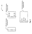
- FIG. 3 illustrates an embodiment 300 of a C3MOS wideband input data amplifier circuit 310 that provides for expanded bandwidth and reduced reflection at the interface of silicon and package and/or circuit board.
- the C3MOS wideband input data amplifier circuit 310 is a first input stage at the interface of package and/or circuit board on one side and silicon on the other side.
- Two differential input pads (shown as 301 and 302) communicatively couple to the C3MOS wideband input data amplifier circuit 310 providing a differential input signal (shown as INP and INN).
- An input matching impedance network 320 is emplaced between the input to the C3MOS wideband input data amplifier circuit 310 and a wideband differential transistor pair 330.
- the input matching impedance network 320 includes two separate input impedances (shown as 321 and 322) that are coupled serially in the two respective paths of the differential input signal and a differential termination impedance 324 that communicatively couples between the two respective paths of the differential input signal.
- the differential termination impedance 324 is located after each of the input impedances 321 and 322.
- the differential output signal of the input matching impedance network 320 is the input to the wideband differential transistor pair 330.
- Two separate output impedances couple between the wideband differential transistor pair 330 and a supply voltage 340 within the C3MOS wideband input data amplifier circuit 310.
- the supply voltage 340 may simply be a node within the C3MOS wideband input data amplifier circuit 310 that receives a power supply's voltage and brings it into the C3MOS wideband input data amplifier circuit 310.
- the differential output signal of the wideband differential transistor pair 330 (which is also the differential output signal of the C3MOS wideband input data amplifier circuit 310) then communicatively couples to one or more other blocks 350 within the same integrated circuit or via appropriate integrated circuit connections to one or more other integrated circuits, circuit boards, blocks and/or devices.
- a designer is provided a great deal of latitude in selecting the individual components of the input matching impedance network 320 in an effort to match the impedance of the package and/or circuit board; this is also true with respect to the individual sub-components of the input matching impedance network 320 (i.e., the input impedances 321 and 322 and the differential termination impedance 324).
- a designer is provided a great deal of latitude in selecting the individual components of the output impedances 331 and 332.
- the C3MOS wideband input data amplifier circuit 310 may also be further improved by replacing the input impedances 321 and 322 (e.g., that may typically be primarily inductive in many embodiments) with an inductive network that includes (multiple) inductor(s), resistor(s) and capacitor(s).
- the design focus idea is to use more elements (i.e., the appropriate number and combination of elements) to match the impedance looking towards board and/or package more precisely within a broader frequency range and at the same time to create a resonant circuit to generate peaking at high frequency so that the bandwidth of the circuit can be extended.
- the overall series resistance in the input impedances 321 and 322 of the matching impedance network 320 (e.g., which may be largely inductive in many instances) needs to be small in order to still have a good impedance matching at the low frequencies and to be able to create effective peaking to extend the bandwidth.
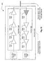
- FIG. 4 illustrates various embodiments 400 of input impedance that may be employed within a C3MOS wideband input data amplifier circuit that has been constructed.
- the input impedances 321 and 322 of the FIG. 3 may be designed in a variety of ways.
- Input impedance 401 includes simply a series connected inductor.
- Input impedance 402 includes a series connected inductor with two separate shunt capacitors location at the two ends of the series connected inductor.
- Input impedance 403 includes two series connected inductors with three separate shunt capacitors location at the nodes generated by the two series connected inductors.
- any number of selected series connected inductors and shunt capacitors may be selected as shown by the input impedance 404 that includes a plurality of series connected inductor with a plurality of shunt capacitors location at the various nodes generated by the plurality of series connected inductors.
- the input impedance 404 that includes a plurality of series connected inductor with a plurality of shunt capacitors location at the various nodes generated by the plurality of series connected inductors.
- FIG. 5 illustrates various embodiments 500 of differential termination impedance that may be employed within a C3MOS wideband input data amplifier circuit that has been constructed.
- the differential termination impedance 324 of the FIG. 3 may be designed in a variety of ways.
- Differential termination impedance 551 includes simply a series connected resistor.
- Differential termination impedance 552 includes a series connected resistor with two separate shunt capacitors location at the two ends of the series connected resistor.
- Differential termination impedance 553 includes two 50 ⁇ series connected resistors; these particular values (e.g., 50 ⁇ ) may be selected in an effort to mach the characteristic impedance of the pads and associated bond wire interfacing of the package and/or circuit board side.
- a low impedance path can be provided to create an AC ground for improved common mode reflection.
- a relatively large capacitor, or other appropriately selected low impedance component combination, can be connected between the shared node of the two 50 ⁇ series connected resistors and ground.
- FIG. 6 illustrates various embodiments 600 of output impedance that may be employed within a C3MOS wideband input data amplifier circuit that has been constructed.
- the output impedances 331 and 332 of the FIG. 3 may be designed in a variety of ways.
- Output impedance 601 includes a series connected resistor and inductor in one order
- output impedance 602 also includes a series connected resistor and inductor but in a reverse order
- Output impedance 603 includes a series connected resistor and inductor the same order as the output impedance 601 while also include a shunt capacitor connected to the node generated at the connection of the series connected resistor and inductor.
- FIG. 7 illustrates another embodiment 700 of a C3MOS wideband input data amplifier circuit that provides for expanded bandwidth and reduced reflection at the interface of silicon and package and/or circuit board.
- a current source transistor may be biased by a bias voltage so that a constant current flows from drain to source in the current source transistor.
- Two separate differential transistors compose a wideband differential transistor pair.
- a first differential transistor has its gate tied to the negative end of a first series peaking inductor L1, while a positive differential input signal INP is coupled to the positive end of the first series peaking inductor L1.
- a second differential transistor has its gate tied to the negative end of a second series peaking inductor L2, while a negative differential input signal INN is coupled to the positive end of the second series peaking inductor L2.
- two series connected 50 ⁇ termination resistors are connected between the gates of the first differential transistor and the second first differential transistor.
- a low impedance path can be provided to create an AC ground for improved common mode reflection.
- a relatively large capacitor (C0) can be connected between the shared node of the termination resistors (i.e., the two series connected 50 ⁇ resistors) and ground.
- a first output resistor R3 has its negative end tied to the drain of the first differential transistor, and has its positive end tied to the negative end of a first shunt peaking inductor L3.
- a second output resistor R4 has its negative end tied to the drain of the second differential transistor, and has its positive end tied to the negative end of a second shunt peaking inductor L4.
- the positive ends of the first and second shunt peaking inductors L3 and L4 are tied to the positive supply voltage (shown as V CC ).
- the first and second output resistors R3 and R4 have the same resistance value R, and the first and second shunt peaking inductors L3 and L4 have the same inductances.
- a first capacitor C1 (which may be referred to as a first Miller cancellation capacitor C1) has its positive end coupled to the drain of the second differential transistor, and has its negative end coupled to the gate of the first differential transistor.
- a second capacitor C2 (which may be referred to as a second Miller cancellation capacitor C2) has its positive end coupled to the drain of the first differential transistor, and has its negative end coupled to the gate of the second differential transistor.
- a first output signal OUTP is taken at the drain of the second differential transistor, and the second output signal OUTN is taken at the drain of the first differential transistor.
- the input inductors also make the input impedance more inductive and thus matching better with the package and/or circuit board. This will help to reduce the reflection at the interface between the silicon and package and/or circuit board.
- FIG. 8A illustrates an embodiment 801 of impedance matching at the interface of silicon 820 and a package and/or circuit board in a single-ended configuration as represented by lumped elements corresponding to the C3MOS wideband data amplifier circuit of the FIG. 2.
- FIG. 8B illustrates an embodiment 802 of impedance matching at the interface of silicon and a package and/or circuit board in a single-ended configuration as represented by lumped elements corresponding to a C3MOS wideband input data amplifier circuit that has been constructed.
- FIG. 8A corresponds to the C3MOS wideband data amplifier circuit of the FIG. 2
- FIG. 8B corresponds to a C3MOS wideband data amplifier circuit having better matched impedance as being designed.
- the impedance matching at the interface of silicon and package and/or circuit board in these diagrams is represented in a single-ended configuration represented by lumped elements for the circuits.
- FIG. 8A When comparing FIG. 8A and the FIG. 8B, it is evident that a circuit, designed in accordance with an embodiment of the invention, provides a much better impedance matching in the single-ended configuration which is applicable to common-mode reflections.
- a circuit designed in accordance with an embodiment of the invention, also reduces the input reflection by matching the impedance looking towards the silicon to the impedance looking towards the board/package, as shown in FIG. 9.
- the input impedances e.g., that may includes 1 or more series connected inductors
- the input impedances should have relatively low series parasitic resistance.
- any inductors employed therein should have a quality factor that is reasonably high. This would also help to extend the bandwidth more effectively because if the quality factor is too low, the resonant peak in the frequency response of the C3MOS wideband input data amplifier circuit will be too small to impact on the overall bandwidth.
- FIG. 9 illustrates an embodiment 900 of impedance matching at the interface of silicon and a package and/or circuit board in a differential mode configuration as represented by lumped elements corresponding to a C3MOS wideband input data amplifier circuit that has been constructed.
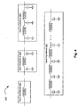
- FIG. 10 illustrates an embodiment 1000 of implementation of one or more C3MOS wideband input data amplifier circuits within a communication transceiver that communicatively couples to a communication network.
- This diagram shows a communication transceiver 1010 that may be implemented in any of a wide variety of communication systems.
- the communication transceiver 1010 may communicatively couple to and communicate with an Ethernet network 1099.
- Such an Ethernet network 1099 may be implemented as a fiber-optic network; generally speaking, the Ethernet network 1099 may also be implemented as a wired network or a combination network that includes both wired and wireless components.
- the communication transceiver 1010 may be implemented to perform bi-directional communication with a wide variety of communication system types.
- the communication transceiver 1010 may be implemented as a single integrated circuit in some embodiments.
- various components of the communication transceiver 1010 and the functional blocks included therein may also be implemented using individual integrated circuits, and these integrated circuits may be integrated together to form a larger module or device that composes the communication transceiver 1010.
- the communication transceiver 1010 Looking at the bi-directional capability of the communication transceiver 1010, it can be seen that there is an upstream and a downstream flow. Looking from another perspective, there in an input flow to the communication transceiver 1010, and there is an output flow from the communication transceiver 1010.
- the output flow within the communication transceiver 1010 may come from 1 or more other blocks (shown as reference numeral 1029) within or outside of the communication transceiver 1010; this flow passes to a transmitter 1020.
- This transmitter 1020 may be simply a functional block within the communication transceiver 1010 (i.e., when the communication transceiver 1010 is implemented as a singular integrated circuit).
- this transmitter 1020 may itself be a distinct integrated circuit that is part of a number of integrated circuits that compose the communication transceiver 1010.
- the input flow to the communication transceiver 1010 comes from the very network to which the communication transceiver 1010 communicatively couples and with which the communication transceiver communicates.
- This input flow to the communication transceiver 1010 passes to 1 or more other blocks (shown as reference numeral 1039) within or outside of the communication transceiver 1010 after having passed through the initial processing component of a receiver 1030.
- this receiver 1030 may be simply a functional block within the communication transceiver 1010 (i.e., when the communication transceiver 1010 is implemented as a singular integrated circuit).
- this receiver 1030 may itself be a distinct integrated circuit that is part of a number of integrated circuits that compose the communication transceiver 1010.
- each of the transmitter 1020 and the receiver 1030 is shown as including a plurality of such stages.
- the transmitter 1020 is shown as having stage 1021, stage 1022, stage 1023, ..., and stage 1024;
- the receiver 1030 is shown as having stage 1031, stage 1032, stage 1033, ..., and stage 1034. Any one of these stages may be implemented according to a C3MOS wideband input data amplifier circuit that has been built.
- stage 1034 of the receiver 1030 (this being the input stage to the communication transceiver 1010)
- this stage 1034 it is the interface indicated by this stage 1034 at which any undesirable and deleterious reflections could arise if there is not appropriate impedance matching.
- C3MOS wideband input data amplifier circuit may be employed at any of the stages indicated within the transmitter 1020 and the receiver 1030 of the communication transceiver 1010, it may be of particular interest in a given application to use such a C3MOS wideband input data amplifier circuit at the stage 1034 of the receiver 1030 of the communication transceiver 1010 to ensure appropriate impedance matching.
- a designer is provided a great deal of latitude in designing an input matching impedance network for a C3MOS wideband input data amplifier circuit (including using inductors, capacitors, and/or resistors) to ensure appropriate impedance matching at this interface thereby reducing (if not eliminating completely) any undesirable and deleterious reflections.
Landscapes
- Engineering & Computer Science (AREA)
- Chemical & Material Sciences (AREA)
- Materials Engineering (AREA)
- Power Engineering (AREA)
- Physics & Mathematics (AREA)
- Organic Chemistry (AREA)
- Spectroscopy & Molecular Physics (AREA)
- Health & Medical Sciences (AREA)
- Medicinal Chemistry (AREA)
- Polymers & Plastics (AREA)
- Chemical Kinetics & Catalysis (AREA)
- Microelectronics & Electronic Packaging (AREA)
- Amplifiers (AREA)
Applications Claiming Priority (2)
| Application Number | Priority Date | Filing Date | Title |
|---|---|---|---|
| US70398005P | 2005-07-29 | 2005-07-29 | |
| US11/320,402 US7362174B2 (en) | 2005-07-29 | 2005-12-28 | Current-controlled CMOS (C3MOS) wideband input data amplifier for reduced differential and common-mode reflection |
Publications (2)
| Publication Number | Publication Date |
|---|---|
| EP1748551A2 true EP1748551A2 (de) | 2007-01-31 |
| EP1748551A3 EP1748551A3 (de) | 2007-08-01 |
Family
ID=37119497
Family Applications (1)
| Application Number | Title | Priority Date | Filing Date |
|---|---|---|---|
| EP06008841A Ceased EP1748551A3 (de) | 2005-07-29 | 2006-04-27 | Stromgesteuerter CMOS (C3MOS) Breitband Datenverstärker mit reduzierten Differential- und Gleichtaktreflexionen |
Country Status (3)
| Country | Link |
|---|---|
| US (1) | US7362174B2 (de) |
| EP (1) | EP1748551A3 (de) |
| TW (1) | TWI334690B (de) |
Cited By (1)
| Publication number | Priority date | Publication date | Assignee | Title |
|---|---|---|---|---|
| EP3148073A1 (de) * | 2015-09-23 | 2017-03-29 | MediaTek Inc. | Vorrichtung zur durchführung von kondensatorverstärkung in einer elektronischen vorrichtung |
Families Citing this family (18)
| Publication number | Priority date | Publication date | Assignee | Title |
|---|---|---|---|---|
| US7830211B2 (en) * | 2005-07-29 | 2010-11-09 | Broadcom Corporation | Input inductive network for sample and hold amplifiers in high speed data converters |
| CN101957534B (zh) * | 2010-09-02 | 2012-05-23 | 上海交通大学 | 基于硅基表面等离子体波导的超宽带光参量放大器 |
| US9019014B2 (en) | 2013-07-29 | 2015-04-28 | King Fahd University Of Petroleum And Minerals | Programmable multi-gain current amplifier |
| TWI539753B (zh) * | 2013-10-07 | 2016-06-21 | 宏碁股份有限公司 | 電子裝置 |
| US9531571B2 (en) * | 2013-12-31 | 2016-12-27 | Hrl Laboratories, Llc | Agile radio architecture |
| US9148087B1 (en) * | 2014-05-16 | 2015-09-29 | Kandou Labs, S.A. | Symmetric is linear equalization circuit with increased gain |
| US9871516B2 (en) * | 2014-06-04 | 2018-01-16 | Lattice Semiconductor Corporation | Transmitting apparatus with source termination |
| CN105449987B (zh) | 2014-09-02 | 2019-06-25 | 台达电子工业股份有限公司 | 电源装置 |
| US20210081013A1 (en) | 2014-09-02 | 2021-03-18 | Delta Electronics, Inc. | Power supply apparatus |
| CN106329930B (zh) * | 2015-07-06 | 2019-02-12 | 台达电子工业股份有限公司 | 功率变换器 |
| US11036269B2 (en) | 2014-09-02 | 2021-06-15 | Delta Electronics (Shanghai) Co., Ltd. | Power module and manufacturing method thereof |
| US10447166B2 (en) | 2015-08-31 | 2019-10-15 | Delta Electronics, Inc. | Power module |
| TWI631820B (zh) | 2015-02-15 | 2018-08-01 | 西凱渥資訊處理科技公司 | 未經供電之開關模組 |
| KR101719310B1 (ko) * | 2015-10-30 | 2017-03-24 | (주)에프씨아이 | 듀얼 동작 모드 전력 증폭기 |
| US9935597B2 (en) * | 2016-05-27 | 2018-04-03 | Xilinx, Inc. | Circuit for and method of receiving an input signal |
| US10862521B1 (en) * | 2019-01-30 | 2020-12-08 | Inphi Corporation | Techniques for programmable gain attenuation in wideband matching networks with enhanced bandwidth |
| EP4264828A4 (de) * | 2021-01-12 | 2024-11-27 | Georgia Tech Research Corporation | Hocheffizienter leistungsverstärker mit doppelansteuerung für anwendungen mit hoher zuverlässigkeit |
| US12199510B2 (en) * | 2022-01-27 | 2025-01-14 | Qualcomm Incorporated | Radio frequency (RF) power amplifier with transformer for improved output power, wideband, and spurious rejection |
Citations (2)
| Publication number | Priority date | Publication date | Assignee | Title |
|---|---|---|---|---|
| US6424194B1 (en) * | 1999-06-28 | 2002-07-23 | Broadcom Corporation | Current-controlled CMOS logic family |
| JP2005073234A (ja) * | 2003-08-07 | 2005-03-17 | Fujitsu Ltd | 差動増幅回路 |
Family Cites Families (184)
| Publication number | Priority date | Publication date | Assignee | Title |
|---|---|---|---|---|
| US3569732A (en) * | 1969-12-15 | 1971-03-09 | Shell Oil Co | Inductanceless igfet frequency doubler |
| US4333020A (en) * | 1979-05-23 | 1982-06-01 | Motorola, Inc. | MOS Latch circuit |
| CA1153076A (en) | 1979-12-10 | 1983-08-30 | General Electric Company | Resonator coupled differential amplifier |
| FR2494465B1 (fr) | 1980-11-14 | 1987-02-13 | Epd Engineering Projectdevelop | Ordinateur de poche |
| US4395774A (en) * | 1981-01-12 | 1983-07-26 | National Semiconductor Corporation | Low power CMOS frequency divider |
| US4449248A (en) * | 1982-02-01 | 1984-05-15 | General Electric Company | Battery saving radio circuit and system |
| JPS5968072A (ja) * | 1982-10-13 | 1984-04-17 | Sharp Corp | 機能変換用小形電子機器 |
| US4599526A (en) * | 1983-05-13 | 1986-07-08 | At&T Bell Laboratories | Clocked latching circuit |
| US4519068A (en) * | 1983-07-11 | 1985-05-21 | Motorola, Inc. | Method and apparatus for communicating variable length messages between a primary station and remote stations of a data communications system |
| US4737975A (en) * | 1984-09-18 | 1988-04-12 | Metrofone, Inc. | Programmable system for interfacing a standard telephone set with a radio transceiver |
| US4731796A (en) * | 1984-10-25 | 1988-03-15 | Stc, Plc | Multi-mode radio transceiver |
| FR2573211B1 (fr) * | 1984-11-09 | 1986-12-12 | Labo Electronique Physique | Comparateur synchronise |
| US4680787A (en) | 1984-11-21 | 1987-07-14 | Motorola, Inc. | Portable radiotelephone vehicular converter and remote handset |
| GB8521159D0 (en) | 1985-08-23 | 1985-10-02 | Pa Consulting Services | Two-way radio communications system |
| US4807282A (en) * | 1985-12-30 | 1989-02-21 | International Business Machines Corp. | Programmable P/C compatible communications card |
| JPH06105884B2 (ja) | 1986-05-06 | 1994-12-21 | 日本電気株式会社 | 無線電話システム |
| US4850009A (en) | 1986-05-12 | 1989-07-18 | Clinicom Incorporated | Portable handheld terminal including optical bar code reader and electromagnetic transceiver means for interactive wireless communication with a base communications station |
| US5239662A (en) | 1986-09-15 | 1993-08-24 | Norand Corporation | System including multiple device communications controller which coverts data received from two different customer transaction devices each using different communications protocols into a single communications protocol |
| US4727309A (en) * | 1987-01-22 | 1988-02-23 | Intel Corporation | Current difference current source |
| KR910008738B1 (ko) | 1987-02-20 | 1991-10-19 | 닛본 덴기 가부시기가이샤 | 밧데리 절약 채널 스캔 기능을 갖고 있는 휴대용 무선 송수신기 |
| US4817115A (en) * | 1987-02-27 | 1989-03-28 | Telxon Corporation | Encoding and decoding system for electronic data communication system |
| US4777657A (en) | 1987-04-01 | 1988-10-11 | Iss Engineering, Inc. | Computer controlled broadband receiver |
| US4804954A (en) * | 1987-04-30 | 1989-02-14 | Motorola, Inc. | Battery saving method for portable communications receivers |
| US5249302A (en) | 1987-10-09 | 1993-09-28 | Motorola, Inc. | Mixed-mode transceiver system |
| JPH0831770B2 (ja) * | 1987-12-25 | 1996-03-27 | 三菱電機株式会社 | 周波数弁別装置 |
| US4970406A (en) | 1987-12-30 | 1990-11-13 | Gazelle Microcircuits, Inc. | Resettable latch circuit |
| US4806796A (en) * | 1988-03-28 | 1989-02-21 | Motorola, Inc. | Active load for emitter coupled logic gate |
| US5055660A (en) | 1988-06-16 | 1991-10-08 | Avicom International, Inc. | Portable transaction monitoring unit for transaction monitoring and security control systems |
| JP2583578B2 (ja) | 1988-07-01 | 1997-02-19 | 三菱電機株式会社 | ポケット電話機 |
| US5117501A (en) * | 1988-08-08 | 1992-05-26 | General Electric Company | Dynamic regrouping in a trunked radio communications system |
| US5087099A (en) * | 1988-09-02 | 1992-02-11 | Stolar, Inc. | Long range multiple point wireless control and monitoring system |
| US4916441A (en) * | 1988-09-19 | 1990-04-10 | Clinicom Incorporated | Portable handheld terminal |
| JP2805767B2 (ja) | 1988-09-26 | 1998-09-30 | 日本電気株式会社 | 無線送受信機 |
| US4894792A (en) * | 1988-09-30 | 1990-01-16 | Tandy Corporation | Portable computer with removable and replaceable add-on modules |
| US5008879B1 (en) * | 1988-11-14 | 2000-05-30 | Datapoint Corp | Lan with interoperative multiple operational capabilities |
| US4995099A (en) * | 1988-12-01 | 1991-02-19 | Motorola, Inc. | Power conservation method and apparatus for a portion of a predetermined signal |
| US5025486A (en) * | 1988-12-09 | 1991-06-18 | Dallas Semiconductor Corporation | Wireless communication system with parallel polling |
| GB2226475A (en) | 1988-12-23 | 1990-06-27 | Philips Electronic Associated | Power economising in multiple user radio systems |
| US5150361A (en) | 1989-01-23 | 1992-09-22 | Motorola, Inc. | Energy saving protocol for a TDM radio |
| US5128938A (en) | 1989-03-03 | 1992-07-07 | Motorola, Inc. | Energy saving protocol for a communication system |
| US5839051A (en) | 1989-03-17 | 1998-11-17 | Technophone Limited | Host radio telephone to directly access a handset NAM through a connecter without requiring the handset controller to be employed |
| US5680633A (en) | 1990-01-18 | 1997-10-21 | Norand Corporation | Modular, portable data processing terminal for use in a radio frequency communication network |
| US6014705A (en) * | 1991-10-01 | 2000-01-11 | Intermec Ip Corp. | Modular portable data processing terminal having a higher layer and lower layer partitioned communication protocol stack for use in a radio frequency communications network |
| US5428636A (en) * | 1993-05-03 | 1995-06-27 | Norand Corporation | Radio frequency local area network |
| US5247656A (en) | 1989-06-01 | 1993-09-21 | Matsushita Electric Industrial Co., Ltd. | Method and apparatus for controlling a clock signal |
| US5029183A (en) | 1989-06-29 | 1991-07-02 | Symbol Technologies, Inc. | Packet data communication network |
| GB2234371A (en) | 1989-07-07 | 1991-01-30 | Inmos Ltd | Clock generation |
| US4969206A (en) | 1989-07-18 | 1990-11-06 | Phyle Industries Limited | Portable data collection device with RF transmission |
| US4964121A (en) | 1989-08-30 | 1990-10-16 | Motorola, Inc. | Battery saver for a TDM system |
| US5121408A (en) * | 1989-10-16 | 1992-06-09 | Hughes Aircraft Company | Synchronization for entry to a network in a frequency hopping communication system |
| AU6721890A (en) * | 1989-11-03 | 1991-05-31 | Microcom Systems, Inc. | Method and apparatus for effecting efficient transmission of data |
| JPH05502130A (ja) * | 1989-11-22 | 1993-04-15 | ラッセル、デヴィッド、シー | コンピューター制御システム |
| US5153878A (en) | 1989-12-11 | 1992-10-06 | Motorola Inc. | Radio data communications system with diverse signaling capability |
| US5055659A (en) | 1990-02-06 | 1991-10-08 | Amtech Technology Corp. | High speed system for reading and writing data from and into remote tags |
| JPH0810995Y2 (ja) | 1990-02-08 | 1996-03-29 | 沖電気工業株式会社 | 自動車電話機用アダプタ |
| CA2077458C (en) | 1990-03-03 | 2001-10-30 | Robert Edmund Todd | Communications system |
| GB2241851A (en) | 1990-03-09 | 1991-09-11 | Philips Electronic Associated | Optimising transmitter power in a communications system |
| US5041740A (en) | 1990-04-30 | 1991-08-20 | Motorola, Inc. | Parallel clocked latch |
| JPH0414314A (ja) * | 1990-05-08 | 1992-01-20 | Toshiba Corp | ソース電極結合形論理回路 |
| US5179666A (en) | 1990-06-07 | 1993-01-12 | Unisys Corporation | Block oriented peripheral device interface |
| US5115151A (en) * | 1990-06-08 | 1992-05-19 | Western Digital Corporation | Triple comparator circuit |
| US5079452A (en) * | 1990-06-29 | 1992-01-07 | Digital Equipment Corporation | High speed ECL latch with clock enable |
| US5363121A (en) | 1990-06-29 | 1994-11-08 | International Business Machines Corporation | Multiple protocol communication interface for distributed transaction processing |
| US5584048A (en) | 1990-08-17 | 1996-12-10 | Motorola, Inc. | Beacon based packet radio standby energy saver |
| US5119502A (en) * | 1990-08-30 | 1992-06-02 | Telefonaktiebolaget L M Ericsson | Periodic system ordered rescan in a cellular communication system |
| JP2646831B2 (ja) * | 1990-10-25 | 1997-08-27 | 日本電気株式会社 | 選択呼出受信機 |
| US5181200A (en) * | 1990-10-29 | 1993-01-19 | International Business Machines Corporation | Handoff method and apparatus for mobile wireless workstation |
| US5265270A (en) | 1990-10-31 | 1993-11-23 | Motorola, Inc. | Method and apparatus for providing power conservation in a communication system |
| US5179721A (en) * | 1990-11-05 | 1993-01-12 | Motorola Inc. | Method for inter operation of a cellular communication system and a trunking communication system |
| EP0559776A1 (de) | 1990-11-26 | 1993-09-15 | Motorola, Inc. | Verfahren und vorrichtung für ein personenrufsystem |
| US5230084A (en) | 1990-12-06 | 1993-07-20 | Motorola, Inc. | Selective call receiver having extended battery saving capability |
| JP2530060B2 (ja) * | 1991-01-17 | 1996-09-04 | 株式会社東芝 | 通信制御装置 |
| US5297144A (en) * | 1991-01-22 | 1994-03-22 | Spectrix Corporation | Reservation-based polling protocol for a wireless data communications network |
| US5265238A (en) | 1991-01-25 | 1993-11-23 | International Business Machines Corporation | Automatic device configuration for dockable portable computers |
| US5134347A (en) | 1991-02-22 | 1992-07-28 | Comfortex Corporation | Low power consumption wireless data transmission and control system |
| US5081402A (en) * | 1991-02-22 | 1992-01-14 | Comfortex Corporation | Low power consumption wireless data transmission and control system |
| US5152006A (en) | 1991-02-25 | 1992-09-29 | Motorola, Inc. | Receiver controller method and apparatus |
| DE69126604T2 (de) * | 1991-03-13 | 1998-01-08 | Ibm | Anpassungseinrichtung und Verfahren zur wirksamen Verbindung von Datenverarbeitungseinrichtungen und Netzwerken |
| CA2040234C (en) * | 1991-04-11 | 2000-01-04 | Steven Messenger | Wireless coupling of devices to wired network |
| US5249220A (en) | 1991-04-18 | 1993-09-28 | Rts Electronics, Inc. | Handheld facsimile and alphanumeric message transceiver operating over telephone or wireless networks |
| JP2930257B2 (ja) | 1991-04-22 | 1999-08-03 | 株式会社東芝 | 携帯可能電子装置 |
| CA2102914A1 (en) * | 1991-05-13 | 1992-11-26 | Robert C. Dixon | Dual mode transmitter and receiver |
| US6374311B1 (en) * | 1991-10-01 | 2002-04-16 | Intermec Ip Corp. | Communication network having a plurality of bridging nodes which transmit a beacon to terminal nodes in power saving state that it has messages awaiting delivery |
| US5394436A (en) * | 1991-10-01 | 1995-02-28 | Norand Corporation | Radio frequency local area network |
| US5940771A (en) | 1991-05-13 | 1999-08-17 | Norand Corporation | Network supporting roaming, sleeping terminals |
| US5123029A (en) * | 1991-06-21 | 1992-06-16 | International Business Machines Corporation | Broadcast-initiated bipartite frame multi-access protocol |
| GB9114808D0 (en) * | 1991-07-09 | 1991-08-28 | Philips Electronic Associated | Information transmission system |
| US5293639A (en) * | 1991-08-09 | 1994-03-08 | Motorola, Inc. | Reduction of power consumption in a portable communication unit |
| US5241542A (en) | 1991-08-23 | 1993-08-31 | International Business Machines Corporation | Battery efficient operation of scheduled access protocol |
| US5361397A (en) | 1991-08-26 | 1994-11-01 | Motorola, Inc. | Communication device and system capable of automatic programmable energizing |
| US5216295A (en) * | 1991-08-30 | 1993-06-01 | General Instrument Corp. | Current mode logic circuits employing IGFETS |
| US5392023A (en) * | 1991-09-06 | 1995-02-21 | Motorola, Inc. | Data communication system with automatic power control |
| US5390206A (en) * | 1991-10-01 | 1995-02-14 | American Standard Inc. | Wireless communication system for air distribution system |
| US5274666A (en) | 1991-10-16 | 1993-12-28 | Telephonics Corporation | Wireless communication system |
| JP2571655B2 (ja) | 1991-11-27 | 1997-01-16 | インターナショナル・ビジネス・マシーンズ・コーポレイション | プロトコル変換機構、交換ネットワーク及びコンピュータ・システム |
| US5440560A (en) | 1991-12-24 | 1995-08-08 | Rypinski; Chandos A. | Sleep mode and contention resolution within a common channel medium access method |
| US5196805A (en) * | 1992-01-31 | 1993-03-23 | Motorola, Inc. | Distributed differential amplifier arrangement |
| US5301196A (en) * | 1992-03-16 | 1994-04-05 | International Business Machines Corporation | Half-speed clock recovery and demultiplexer circuit |
| ATE207679T1 (de) * | 1992-04-20 | 2001-11-15 | 3Com Corp | Vorrichtung zur netzmittelerweiterung auf entfernte netzwerke |
| US5744366A (en) * | 1992-05-01 | 1998-04-28 | Trustees Of The University Of Pennsylvania | Mesoscale devices and methods for analysis of motile cells |
| EP0576690B1 (de) * | 1992-05-26 | 1999-11-17 | Hewlett-Packard GmbH | Einrichtung zur Änderung der Impulsübergangszeit |
| ATE173877T1 (de) | 1992-06-29 | 1998-12-15 | Elonex Technologies Inc | Modular tragbarer rechner |
| US5579487A (en) | 1992-10-02 | 1996-11-26 | Teletransaction, Inc. | Portable work slate computer with multiple docking positions for interchangeably receiving removable modules |
| EP0590818A3 (en) | 1992-10-02 | 1994-05-11 | Nat Semiconductor Corp | Ecl-to-bicmos/cmos translator |
| JPH06162782A (ja) | 1992-11-17 | 1994-06-10 | Hitachi Ltd | 半導体集積回路装置 |
| US5289055A (en) * | 1992-11-17 | 1994-02-22 | At&T Bell Laboratories | Digital ECL bipolar logic gates suitable for low-voltage operation |
| US5426637A (en) * | 1992-12-14 | 1995-06-20 | International Business Machines Corporation | Methods and apparatus for interconnecting local area networks with wide area backbone networks |
| US5373149A (en) | 1993-02-01 | 1994-12-13 | At&T Bell Laboratories | Folding electronic card assembly |
| US5406643A (en) * | 1993-02-11 | 1995-04-11 | Motorola, Inc. | Method and apparatus for selecting between a plurality of communication paths |
| JP2826433B2 (ja) * | 1993-02-26 | 1998-11-18 | 日本電気株式会社 | アンテナ用二周波整合回路 |
| AU690099B2 (en) | 1993-03-04 | 1998-04-23 | Telefonaktiebolaget Lm Ericsson (Publ) | Modular radio communications system |
| WO1994022220A1 (en) * | 1993-03-24 | 1994-09-29 | Apple Computer, Inc. | Differential- to single-ended cmos converter |
| US5630061A (en) * | 1993-04-19 | 1997-05-13 | International Business Machines Corporation | System for enabling first computer to communicate over switched network with second computer located within LAN by using media access control driver in different modes |
| US5796727A (en) | 1993-04-30 | 1998-08-18 | International Business Machines Corporation | Wide-area wireless lan access |
| US5438329A (en) | 1993-06-04 | 1995-08-01 | M & Fc Holding Company, Inc. | Duplex bi-directional multi-mode remote instrument reading and telemetry system |
| US5444763A (en) * | 1993-06-17 | 1995-08-22 | Research In Motion Limited | Translation and connection device for radio frequency point of sale transaction systems |
| US5459412A (en) | 1993-07-01 | 1995-10-17 | National Semiconductor Corporation | BiCMOS circuit for translation of ECL logic levels to MOS logic levels |
| US5418837A (en) * | 1993-07-30 | 1995-05-23 | Ericsson-Ge Mobile Communications Inc. | Method and apparatus for upgrading cellular mobile telephones |
| US5406615A (en) * | 1993-08-04 | 1995-04-11 | At&T Corp. | Multi-band wireless radiotelephone operative in a plurality of air interface of differing wireless communications systems |
| US5544222A (en) | 1993-11-12 | 1996-08-06 | Pacific Communication Sciences, Inc. | Cellular digtial packet data mobile data base station |
| FR2714550B1 (fr) * | 1993-12-24 | 1996-02-02 | Bull Sa | Arbre de portes logiques OU-Exclusif et multiplieur de fréquence l'incorporant. |
| US5510748A (en) * | 1994-01-18 | 1996-04-23 | Vivid Semiconductor, Inc. | Integrated circuit having different power supplies for increased output voltage range while retaining small device geometries |
| US5420529A (en) * | 1994-05-19 | 1995-05-30 | Northern Telecom Limited | Current steering switch and hybrid BiCMOS multiplexer with CMOS commutation signal and CML/ECL data signals |
| CA2124745C (en) | 1994-05-31 | 2001-11-20 | Pmc-Sierra Ltd. | High-speed cmos pseudo-ecl output driver |
| JPH07326936A (ja) | 1994-06-02 | 1995-12-12 | Mitsubishi Electric Corp | 差動増幅器 |
| US5714904A (en) | 1994-06-06 | 1998-02-03 | Sun Microsystems, Inc. | High speed serial link for fully duplexed data communication |
| US5465060A (en) | 1994-06-10 | 1995-11-07 | International Business Machines Corporation | Fast edge triggered self-resetting CMOS receiver with parallel L1/L2 (Master/Slave) latch |
| JP2713167B2 (ja) * | 1994-06-14 | 1998-02-16 | 日本電気株式会社 | 比較器 |
| US5600267A (en) * | 1994-06-24 | 1997-02-04 | Cypress Semiconductor Corporation | Apparatus for a programmable CML to CMOS translator for power/speed adjustment |
| US5521530A (en) * | 1994-08-31 | 1996-05-28 | Oki Semiconductor America, Inc. | Efficient method and resulting structure for integrated circuits with flexible I/O interface and power supply voltages |
| JPH08335860A (ja) * | 1995-06-08 | 1996-12-17 | Mitsubishi Electric Corp | 差動ラッチ回路 |
| US5798658A (en) | 1995-06-15 | 1998-08-25 | Werking; Paul M. | Source-coupled logic with reference controlled inputs |
| KR0170311B1 (ko) | 1995-06-23 | 1999-02-01 | 김광호 | 스태틱 랜덤 억세스 메모리 및 그 제조방법 |
| JPH09153741A (ja) * | 1995-09-13 | 1997-06-10 | Fujitsu Ltd | 変調器、間接変調型変調器、及び周波数逓倍器 |
| JP3149759B2 (ja) * | 1995-11-17 | 2001-03-26 | 日本電気株式会社 | ラッチ回路 |
| US5640356A (en) * | 1995-12-29 | 1997-06-17 | Cypress Semiconductor Corp. | Two-stage differential sense amplifier with positive feedback in the first and second stages |
| US5793225A (en) * | 1996-01-02 | 1998-08-11 | Pmc-Sierra, Inc. | CMOS SONET/ATM receiver suitable for use with pseudo ECL and TTL signaling environments |
| US5724361A (en) * | 1996-03-12 | 1998-03-03 | Lsi Logic Corporation | High performance n:1 multiplexer with overlap control of multi-phase clocks |
| US5821809A (en) | 1996-05-23 | 1998-10-13 | International Business Machines Corporation | CMOS high-speed differential to single-ended converter circuit |
| US5767699A (en) * | 1996-05-28 | 1998-06-16 | Sun Microsystems, Inc. | Fully complementary differential output driver for high speed digital communications |
| US5859881A (en) * | 1996-06-07 | 1999-01-12 | International Business Machines Corporation | Adaptive filtering method and apparatus to compensate for a frequency difference between two clock sources |
| US5903176A (en) * | 1996-09-04 | 1999-05-11 | Litton Systems, Inc. | Clock circuit for generating a high resolution output from a low resolution clock |
| JP3681497B2 (ja) | 1997-03-05 | 2005-08-10 | 株式会社ルネサステクノロジ | フリップフロップ回路、シフトレジスタ回路、直列−並列変換回路、並列−直列変換回路およびラッチ回路 |
| JP3715066B2 (ja) * | 1997-03-25 | 2005-11-09 | 三菱電機株式会社 | 電流モードロジック回路 |
| JP3060987B2 (ja) | 1997-03-31 | 2000-07-10 | 日本電気株式会社 | クロック同期式フリップフロップ回路 |
| GB9707349D0 (en) * | 1997-04-11 | 1997-05-28 | Univ Waterloo | A dynamic current mode logic family |
| US5945847A (en) | 1997-05-20 | 1999-08-31 | Lucent Technologies | Distributed amplifier logic designs |
| US5945863A (en) | 1997-06-18 | 1999-08-31 | Applied Micro Circuits Corporation | Analog delay circuit |
| US6194950B1 (en) * | 1997-08-28 | 2001-02-27 | Lucent Technologies Inc. | High-speed CMOS multiplexer |
| US6014041A (en) * | 1997-09-26 | 2000-01-11 | Intel Corporation | Differential current switch logic gate |
| US6037841A (en) * | 1997-10-07 | 2000-03-14 | Applied Micro Circuits Corporation | Impedance matched CMOS transimpedance amplifier for high-speed fiber optic communications |
| US6061747A (en) * | 1997-10-16 | 2000-05-09 | Lsi Logic Corporation | System for sending data from-and-to a computer monitor using a high speed serial line |
| US6002279A (en) | 1997-10-24 | 1999-12-14 | G2 Networks, Inc. | Clock recovery circuit |
| US6188339B1 (en) * | 1998-01-23 | 2001-02-13 | Fuji Photo Film Co., Ltd. | Differential multiplexer and differential logic circuit |
| FI107657B (fi) | 1998-03-11 | 2001-09-14 | Nokia Mobile Phones Ltd | Kytkentä differentiaalisen aktiivikomponentin impedanssin säätämiseksi |
| US6037842A (en) * | 1998-04-21 | 2000-03-14 | Applied Micro Circuits Corporation | Complementary metal-oxide semiconductor voltage controlled oscillator (CMOS VCO) |
| JPH11346130A (ja) * | 1998-06-02 | 1999-12-14 | Mitsubishi Electric Corp | 半導体装置 |
| US6222380B1 (en) * | 1998-06-15 | 2001-04-24 | International Business Machines Corporation | High speed parallel/serial link for data communication |
| US20020089353A1 (en) | 1998-07-13 | 2002-07-11 | Abdellatif Bellaouar | Current mode logic gates for low-voltage high-speed applications |
| US6094074A (en) | 1998-07-16 | 2000-07-25 | Seiko Epson Corporation | High speed common mode logic circuit |
| US6114843A (en) | 1998-08-18 | 2000-09-05 | Xilinx, Inc. | Voltage down converter for multiple voltage levels |
| US6463092B1 (en) | 1998-09-10 | 2002-10-08 | Silicon Image, Inc. | System and method for sending and receiving data signals over a clock signal line |
| US6111425A (en) | 1998-10-15 | 2000-08-29 | International Business Machines Corporation | Very low power logic circuit family with enhanced noise immunity |
| JP3510507B2 (ja) | 1998-11-27 | 2004-03-29 | Necマイクロシステム株式会社 | ラッチ回路 |
| US6188294B1 (en) | 1999-05-12 | 2001-02-13 | Parthus Technologies, Plc. | Method and apparatus for random sequence generator |
| US6232844B1 (en) * | 1999-05-28 | 2001-05-15 | Vitesse Semiconductor Corporation | Controlled orthogonal current oscillator with ranging |
| US6081162A (en) * | 1999-06-17 | 2000-06-27 | Intel Corporation | Robust method and apparatus for providing a digital single-ended output from a differential input |
| FR2798016B1 (fr) * | 1999-08-31 | 2002-03-29 | St Microelectronics Sa | Circuit amplificateur a double bande passante et tete de reception radiofrequence |
| US6265944B1 (en) | 1999-09-27 | 2001-07-24 | Conexant Systems, Inc. | Fully integrated broadband RF voltage amplifier with enhanced voltage gain and method |
| US7555263B1 (en) | 1999-10-21 | 2009-06-30 | Broadcom Corporation | Adaptive radio transceiver |
| KR100356022B1 (ko) | 1999-11-23 | 2002-10-18 | 한국전자통신연구원 | 씨모스 가변이득 앰프 및 그 제어 방법 |
| US6259320B1 (en) | 1999-12-27 | 2001-07-10 | Nortel Networks Limited | Error correction within power amplifiers |
| US6340899B1 (en) * | 2000-02-24 | 2002-01-22 | Broadcom Corporation | Current-controlled CMOS circuits with inductive broadbanding |
| US6566720B2 (en) * | 2000-10-05 | 2003-05-20 | United Memories, Inc. | Base cell layout permitting rapid layout with minimum clock line capacitance on CMOS standard-cell and gate-array integrated circuits |
| WO2002039582A2 (en) * | 2000-11-09 | 2002-05-16 | Broadcom Corporation | A constant impedance filter |
| US6864558B2 (en) * | 2001-05-17 | 2005-03-08 | Broadcom Corporation | Layout technique for C3MOS inductive broadbanding |
| US6586996B2 (en) * | 2001-08-15 | 2003-07-01 | Broadcom Corporation | Method and system for producing a drive signal for a current steering amplifier |
| US6624699B2 (en) | 2001-10-25 | 2003-09-23 | Broadcom Corporation | Current-controlled CMOS wideband data amplifier circuits |
| US6891436B2 (en) * | 2002-09-30 | 2005-05-10 | Integrant Technologies Inc. | Transconductance varying circuit of transconductor circuit, varying bandwidth filter circuit using the same and digital tuning circuit of transconductor-capacitor filter |
| US6774721B1 (en) | 2003-03-07 | 2004-08-10 | Quake Technologies, Inc. | High speed logic circuits |
| EP1480333A3 (de) | 2003-05-22 | 2006-05-03 | Matsushita Electric Industrial Co., Ltd. | Differentieller Hochfrequenzverstärker, differentieller Mischer, differentieller Oszillator und Hochfrequenzschaltung, welche diese verwendet |
| US6888369B1 (en) * | 2003-07-17 | 2005-05-03 | Altera Corporation | Programmable on-chip differential termination impedance |
| JP2005142633A (ja) * | 2003-11-04 | 2005-06-02 | Mitsubishi Electric Corp | 差動増幅回路および多段増幅回路 |
| TWI269524B (en) * | 2004-11-08 | 2006-12-21 | Richwave Technology Corp | Low noise and high gain low noise amplifier |
-
2005
- 2005-12-28 US US11/320,402 patent/US7362174B2/en not_active Expired - Lifetime
-
2006
- 2006-04-27 EP EP06008841A patent/EP1748551A3/de not_active Ceased
- 2006-07-28 TW TW095127713A patent/TWI334690B/zh not_active IP Right Cessation
Patent Citations (3)
| Publication number | Priority date | Publication date | Assignee | Title |
|---|---|---|---|---|
| US6424194B1 (en) * | 1999-06-28 | 2002-07-23 | Broadcom Corporation | Current-controlled CMOS logic family |
| JP2005073234A (ja) * | 2003-08-07 | 2005-03-17 | Fujitsu Ltd | 差動増幅回路 |
| US20050104661A1 (en) * | 2003-08-07 | 2005-05-19 | Hiroyuki Rokugawa | Differential amplifier |
Non-Patent Citations (1)
| Title |
|---|
| DAVID J CASSAN ET AL: "A 1-V Transformer-Feedback Low-Noise Amplifier for 5-GHz Wireless LAN in 0.18-mu m CMOS", IEEE JOURNAL OF SOLID-STATE CIRCUITS, IEEE SERVICE CENTER, PISCATAWAY, NJ, USA, vol. 38, no. 3, 1 March 2003 (2003-03-01), XP011065964, ISSN: 0018-9200 * |
Cited By (2)
| Publication number | Priority date | Publication date | Assignee | Title |
|---|---|---|---|---|
| EP3148073A1 (de) * | 2015-09-23 | 2017-03-29 | MediaTek Inc. | Vorrichtung zur durchführung von kondensatorverstärkung in einer elektronischen vorrichtung |
| US9800219B2 (en) | 2015-09-23 | 2017-10-24 | Mediatek Inc. | Apparatus for performing capacitor amplification in an electronic device |
Also Published As
| Publication number | Publication date |
|---|---|
| US7362174B2 (en) | 2008-04-22 |
| TWI334690B (en) | 2010-12-11 |
| TW200721663A (en) | 2007-06-01 |
| US20070024369A1 (en) | 2007-02-01 |
| EP1748551A3 (de) | 2007-08-01 |
Similar Documents
| Publication | Publication Date | Title |
|---|---|---|
| US7362174B2 (en) | Current-controlled CMOS (C3MOS) wideband input data amplifier for reduced differential and common-mode reflection | |
| US7902924B2 (en) | Current-controlled CMOS (C3MOS) fully differential integrated wideband amplifier/equalizer with adjustable gain and frequency response without additional power or loading | |
| US6624699B2 (en) | Current-controlled CMOS wideband data amplifier circuits | |
| US6748204B1 (en) | Mixer noise reduction technique | |
| US7935990B2 (en) | RF power amplifier and method for packaging the same | |
| US6636119B2 (en) | Compact cascode radio frequency CMOS power amplifier | |
| US6946849B1 (en) | Circuit for calibrating a resistance | |
| US20100019817A1 (en) | Current-controlled CMOS (C3MOS) fully differential integrated delay cell with variable delay and high bandwidth | |
| US7091791B1 (en) | Transformer implementation using bonding wires | |
| US11094652B1 (en) | Configurable radio transceiver and method thereof | |
| US7113045B2 (en) | Power amplifier input structure having a differential output | |
| US8437723B2 (en) | Amplifier circuit and communication device | |
| US7161427B2 (en) | Input structure for a power amplifier and associated methods | |
| CN211791450U (zh) | 一种功率放大器及功率放大器系统 | |
| US11233393B2 (en) | IC chip | |
| US8406710B1 (en) | Method and apparatus of minimizing extrinsic parasitic resistance in 60 GHz power amplifier circuits | |
| US7830211B2 (en) | Input inductive network for sample and hold amplifiers in high speed data converters | |
| JP6515493B2 (ja) | 増幅回路の帯域幅を改善するための方法及び回路 | |
| EP1246367A2 (de) | Integrierte Halbleiterschaltung und Verfahren zu deren Herstellung | |
| CN100472947C (zh) | 电流控制硅互补金属氧化物半导体宽带数据放大器电路 | |
| EP4738699A1 (de) | Transformatorbasierte vorspannungsschaltung für gegentaktfrequenzverdoppler | |
| Toh et al. | Wide-band, low-noise, matched-impedance amplifiers in submicrometer MOS technology | |
| US12199510B2 (en) | Radio frequency (RF) power amplifier with transformer for improved output power, wideband, and spurious rejection | |
| US20240048109A1 (en) | Signal termination for amplifiers | |
| US20210344095A1 (en) | Directional coupler and semiconductor chip |
Legal Events
| Date | Code | Title | Description |
|---|---|---|---|
| PUAI | Public reference made under article 153(3) epc to a published international application that has entered the european phase |
Free format text: ORIGINAL CODE: 0009012 |
|
| AK | Designated contracting states |
Kind code of ref document: A2 Designated state(s): AT BE BG CH CY CZ DE DK EE ES FI FR GB GR HU IE IS IT LI LT LU LV MC NL PL PT RO SE SI SK TR |
|
| AX | Request for extension of the european patent |
Extension state: AL BA HR MK YU |
|
| RAP1 | Party data changed (applicant data changed or rights of an application transferred) |
Owner name: BROADCOM CORPORATION |
|
| PUAL | Search report despatched |
Free format text: ORIGINAL CODE: 0009013 |
|
| AK | Designated contracting states |
Kind code of ref document: A3 Designated state(s): AT BE BG CH CY CZ DE DK EE ES FI FR GB GR HU IE IS IT LI LT LU LV MC NL PL PT RO SE SI SK TR |
|
| AX | Request for extension of the european patent |
Extension state: AL BA HR MK YU |
|
| 17P | Request for examination filed |
Effective date: 20080201 |
|
| 17Q | First examination report despatched |
Effective date: 20080303 |
|
| AKX | Designation fees paid |
Designated state(s): DE FR GB |
|
| RAP1 | Party data changed (applicant data changed or rights of an application transferred) |
Owner name: AVAGO TECHNOLOGIES GENERAL IP (SINGAPORE) PTE. LTD |
|
| RAP1 | Party data changed (applicant data changed or rights of an application transferred) |
Owner name: AVAGO TECHNOLOGIES INTERNATIONAL SALES PTE. LIMITE |
|
| STAA | Information on the status of an ep patent application or granted ep patent |
Free format text: STATUS: THE APPLICATION HAS BEEN REFUSED |
|
| 18R | Application refused |
Effective date: 20181212 |