EP1749794A2 - Gehäusestruktur für elektronische Bauteile und dessen Herstellungsverfahren - Google Patents
Gehäusestruktur für elektronische Bauteile und dessen Herstellungsverfahren Download PDFInfo
- Publication number
- EP1749794A2 EP1749794A2 EP06253650A EP06253650A EP1749794A2 EP 1749794 A2 EP1749794 A2 EP 1749794A2 EP 06253650 A EP06253650 A EP 06253650A EP 06253650 A EP06253650 A EP 06253650A EP 1749794 A2 EP1749794 A2 EP 1749794A2
- Authority
- EP
- European Patent Office
- Prior art keywords
- electronic parts
- silicon
- sealing cap
- packaging structure
- circuit substrate
- Prior art date
- Legal status (The legal status is an assumption and is not a legal conclusion. Google has not performed a legal analysis and makes no representation as to the accuracy of the status listed.)
- Withdrawn
Links
Images




Classifications
-
- B—PERFORMING OPERATIONS; TRANSPORTING
- B81—MICROSTRUCTURAL TECHNOLOGY
- B81C—PROCESSES OR APPARATUS SPECIALLY ADAPTED FOR THE MANUFACTURE OR TREATMENT OF MICROSTRUCTURAL DEVICES OR SYSTEMS
- B81C1/00—Manufacture or treatment of devices or systems in or on a substrate
- B81C1/00015—Manufacture or treatment of devices or systems in or on a substrate for manufacturing microsystems
- B81C1/00261—Processes for packaging MEMS devices
- B81C1/00301—Connecting electric signal lines from the MEMS device with external electrical signal lines, e.g. through vias
-
- H—ELECTRICITY
- H10—SEMICONDUCTOR DEVICES; ELECTRIC SOLID-STATE DEVICES NOT OTHERWISE PROVIDED FOR
- H10F—INORGANIC SEMICONDUCTOR DEVICES SENSITIVE TO INFRARED RADIATION, LIGHT, ELECTROMAGNETIC RADIATION OF SHORTER WAVELENGTH OR CORPUSCULAR RADIATION
- H10F39/00—Integrated devices, or assemblies of multiple devices, comprising at least one element covered by group H10F30/00, e.g. radiation detectors comprising photodiode arrays
- H10F39/80—Constructional details of image sensors
- H10F39/804—Containers or encapsulations
-
- H—ELECTRICITY
- H10—SEMICONDUCTOR DEVICES; ELECTRIC SOLID-STATE DEVICES NOT OTHERWISE PROVIDED FOR
- H10W—GENERIC PACKAGES, INTERCONNECTIONS, CONNECTORS OR OTHER CONSTRUCTIONAL DETAILS OF DEVICES COVERED BY CLASS H10
- H10W20/00—Interconnections in chips, wafers or substrates
- H10W20/01—Manufacture or treatment
- H10W20/021—Manufacture or treatment of interconnections within wafers or substrates
- H10W20/023—Manufacture or treatment of interconnections within wafers or substrates the interconnections being through-semiconductor vias
-
- H—ELECTRICITY
- H10—SEMICONDUCTOR DEVICES; ELECTRIC SOLID-STATE DEVICES NOT OTHERWISE PROVIDED FOR
- H10W—GENERIC PACKAGES, INTERCONNECTIONS, CONNECTORS OR OTHER CONSTRUCTIONAL DETAILS OF DEVICES COVERED BY CLASS H10
- H10W20/00—Interconnections in chips, wafers or substrates
- H10W20/01—Manufacture or treatment
- H10W20/021—Manufacture or treatment of interconnections within wafers or substrates
- H10W20/023—Manufacture or treatment of interconnections within wafers or substrates the interconnections being through-semiconductor vias
- H10W20/0261—Manufacture or treatment of interconnections within wafers or substrates the interconnections being through-semiconductor vias characterised by the filling method or the material of the conductive fill
-
- H—ELECTRICITY
- H10—SEMICONDUCTOR DEVICES; ELECTRIC SOLID-STATE DEVICES NOT OTHERWISE PROVIDED FOR
- H10W—GENERIC PACKAGES, INTERCONNECTIONS, CONNECTORS OR OTHER CONSTRUCTIONAL DETAILS OF DEVICES COVERED BY CLASS H10
- H10W70/00—Package substrates; Interposers; Redistribution layers [RDL]
- H10W70/60—Insulating or insulated package substrates; Interposers; Redistribution layers
- H10W70/67—Insulating or insulated package substrates; Interposers; Redistribution layers characterised by their insulating layers or insulating parts
- H10W70/69—Insulating materials thereof
- H10W70/698—Semiconductor materials that are electrically insulating, e.g. undoped silicon
-
- H—ELECTRICITY
- H10—SEMICONDUCTOR DEVICES; ELECTRIC SOLID-STATE DEVICES NOT OTHERWISE PROVIDED FOR
- H10W—GENERIC PACKAGES, INTERCONNECTIONS, CONNECTORS OR OTHER CONSTRUCTIONAL DETAILS OF DEVICES COVERED BY CLASS H10
- H10W76/00—Containers; Fillings or auxiliary members therefor; Seals
- H10W76/10—Containers or parts thereof
- H10W76/12—Containers or parts thereof characterised by their shape
- H10W76/15—Containers comprising an insulating or insulated base
- H10W76/153—Containers comprising an insulating or insulated base having interconnections in passages through the insulating or insulated base
-
- B—PERFORMING OPERATIONS; TRANSPORTING
- B81—MICROSTRUCTURAL TECHNOLOGY
- B81B—MICROSTRUCTURAL DEVICES OR SYSTEMS, e.g. MICROMECHANICAL DEVICES
- B81B2207/00—Microstructural systems or auxiliary parts thereof
- B81B2207/09—Packages
- B81B2207/091—Arrangements for connecting external electrical signals to mechanical structures inside the package
- B81B2207/094—Feed-through, via
- B81B2207/096—Feed-through, via through the substrate
-
- B—PERFORMING OPERATIONS; TRANSPORTING
- B81—MICROSTRUCTURAL TECHNOLOGY
- B81C—PROCESSES OR APPARATUS SPECIALLY ADAPTED FOR THE MANUFACTURE OR TREATMENT OF MICROSTRUCTURAL DEVICES OR SYSTEMS
- B81C2203/00—Forming microstructural systems
- B81C2203/01—Packaging MEMS
- B81C2203/0109—Bonding an individual cap on the substrate
-
- H—ELECTRICITY
- H10—SEMICONDUCTOR DEVICES; ELECTRIC SOLID-STATE DEVICES NOT OTHERWISE PROVIDED FOR
- H10P—GENERIC PROCESSES OR APPARATUS FOR THE MANUFACTURE OR TREATMENT OF DEVICES COVERED BY CLASS H10
- H10P14/00—Formation of materials, e.g. in the shape of layers or pillars
- H10P14/40—Formation of materials, e.g. in the shape of layers or pillars of conductive or resistive materials
- H10P14/46—Formation of materials, e.g. in the shape of layers or pillars of conductive or resistive materials using a liquid
- H10P14/47—Electrolytic deposition, i.e. electroplating; Electroless plating
-
- H—ELECTRICITY
- H10—SEMICONDUCTOR DEVICES; ELECTRIC SOLID-STATE DEVICES NOT OTHERWISE PROVIDED FOR
- H10W—GENERIC PACKAGES, INTERCONNECTIONS, CONNECTORS OR OTHER CONSTRUCTIONAL DETAILS OF DEVICES COVERED BY CLASS H10
- H10W90/00—Package configurations
- H10W90/701—Package configurations characterised by the relative positions of pads or connectors relative to package parts
- H10W90/721—Package configurations characterised by the relative positions of pads or connectors relative to package parts of bump connectors
- H10W90/724—Package configurations characterised by the relative positions of pads or connectors relative to package parts of bump connectors between a chip and a stacked insulating package substrate, interposer or RDL
Definitions
- the present invention relates to an electronic parts packaging structure and a method of manufacturing the same. More specifically, the present invention relates to an electronic parts packaging structure having a structure in which an electronic part is mounted in a state that the electronic part is hermetically sealed with a sealing cap, and relates to a method of manufacturing the same.
- Patent Literature 1 Japanese Unexamined Patent Publication No. 2000-235044 , an acceleration sensor having a structure in which a glass cap is bonded to the top of a sensor chip is described, and a recessed portion is formed in the glass cap in order to ensure a space for the swinging of a weighting portion.
- Patent Document 2 Japanese Unexamined Patent Publication No. 2001-7346 .
- a method of manufacturing an external force sensor (Fig. 1) is described, and it is described that after a sensor device is made by anodically bonding a device substrate having a recessed portion provided in a lower central portion thereof to a supporting substrate and by forming through holes in the device substrate, a lid portion made of glass which includes a recessed portion may be further provided on the device substrate by anodic bonding.
- interposers on which various electronic parts are mounted or formed silicon substrates are used instead of ceramic substrates and glass epoxy resins to meet a demand for higher densities.
- interposers which have a structure in which through electrodes are provided in a silicon substrate to enable conduction between the two sides of the silicon substrate are proposed.
- a sealing cap can be provided on a silicon substrate (interposer) having a through electrode provided therein with a high level of reliability, and to provide a method of manufacturing the same.
- an electronic parts packaging structure including: a silicon circuit substrate having a structure in which wiring layers on both sides thereof are connected to each other through a through electrode; an electronic part mounted or formed on the silicon circuit substrate; and a sealing cap including a ring-shaped protruded bonding portion in which at least a bonding part thereof is made of glass, and having a structure in which a cavity (50a) is constituted by the protruded bonding portion (50b), the protruded bonding portion of the sealing cap is bonded to a bonding portion of the silicon circuit substrate, wherein the electronic part is hermetically sealed in the cavity of the sealing cap.
- the silicon circuit substrate is used as an interposer, the through electrode is provided in the silicon circuit substrate, and the wiring layers on both sides of the silicon circuit substrate are connected to each other via the through electrode.
- the electronic parts semiconductor device, imaging device, or MEMS device
- the bonding portion where the substrate is exposed is provided in the silicon substrate outside the electronic parts.
- the protruded bonding portion (glass) of the sealing cap in which the ring-shaped protruded bonding portion and the cavity are provided, is anodically bonded to the bonding portion of the silicon circuit substrate.
- the use of the silicon circuit substrate in an embodiment of the present invention makes it possible to form high-density wiring.
- the provision of the through electrodes reduces wiring length, and makes it possible to easily cope with a higher-speed electronic parts.
- the sealing cap can be easily provided on the silicon circuit substrate by bonding. Accordingly, even in the case where an electronic parts is mounted of which reliability is impaired by moisture or the like from outside air, the electronic parts can be easily hermetically sealed to improve the reliability thereof.
- the silicon circuit substrate is used as an interposer, the thermal expansion coefficients of the electronic parts (silicon chip) and the interposer can be set equal to each other. Accordingly, the occurrence of thermal stresses is suppressed. This makes it possible to improve the reliability of a semiconductor device even in the case where an electronic parts (silicon chip) vulnerable to stresses is mounted.
- the electronic parts mounted or formed on the silicon circuit substrate having the through electrode provided therein can be easily hermetically sealed with the sealing cap. Accordingly, the reliability of the electronic parts can be improved.
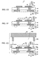
- Figs. 1A to 1Q are cross-sectional views showing a method of manufacturing an electronic parts packaging structure of a first embodiment of the present invention
- Fig. 2 is a cross-sectional view showing the electronic parts packaging structure of the first embodiment.
- a silicon wafer 10 having a thickness of approximately 625 ⁇ m is prepared as a silicon substrate.
- one surface of the silicon wafer 10 is ground by a back grinder (BG), thus obtaining the silicon wafer 10 the thickness of which is reduced to 50 to 300 ⁇ m (preferably approximately 200 ⁇ m).
- BG back grinder
- a plurality of device mounting regions or device forming regions
- the silicon wafer 10 is divided in a later step, and individual electronic parts packaging structures are obtained.
- through holes 10a penetrating the silicon wafer 10 in the thickness direction thereof are formed by forming on the silicon wafer 10 a mask (not shown) having opening portions provided therein, and by etching the silicon substrate 10 through the opening portions by RIE.
- the diameters of the through holes 10a are set in the range of, for example, 30 to 60 ⁇ m. Subsequently, the mask is removed.
- an insulating layer 12 made of a silicon oxide layer which has a thickness of approximately 500 nm is formed on both surfaces of the silicon wafer 10 and the inner surfaces of the through holes 10a by thermally oxidizing the silicon wafer 10.
- a silicon oxide layer or a silicon nitride layer may be formed by CVD on the entire surface of the silicon wafer 10 to be used as the insulating layer 12.
- an opening portion 12a is formed in the insulating layer 12 by forming a resist film (not shown) having a ring-shaped opening portion provided in a peripheral portion of each device mounting region of the silicon wafer 10, and by etching the insulating layer 12 through the opening portion using buffered hydrofluoric acid or the like.
- the silicon wafer 10 is exposed in a ring shape in the peripheral portion of each device mounting region of the silicon wafer 10 to serve as a bonding portion 10b.
- the resist film is removed.
- the bonding portion 10b of the silicon wafer 10 is formed in order to anodically bond a sealing cap (glass) to the peripheral portion of each device mounting region of the silicon wafer 10, as described later.
- copper foil 14 is glued onto the lower surface of the silicon wafer 10 with an adhesive material 13, and then the adhesive material 13 under the through holes 10a of the silicon wafer 10 is removed by ashing to expose the copper foil 14 at the bottoms of the through holes 10a. In this way, the silicon wafer 10 including the through holes 10a is placed on the copper foil 14.
- through electrodes 16 are formed by performing metal (Cu) plating on the through holes 10a of the silicon wafer 10 from lower portions thereof to upper portions thereof by electroplating using the copper foil 14 as a plating power-supplying layer. Then, as shown in Fig. 1H, the copper foil 14 and the adhesive material 13 are removed from the silicon wafer 10. The copper foil 14 is etched by an H 2 SO 4 /H 2 O 2 solution to be removed, and the adhesive material 13 is removed by ashing.
- Cu metal
- the upper and lower portions of the through electrodes 16 which protrude from the upper and the lower surfaces of the silicon wafer 10 are removed by polishing, thus planarizing the upper and the lower sides of the silicon wafer 10.
- a chromium (Cr) layer having a film thickness of 50 nm and a copper (Cu) layer having a film thickness of 750 nm are sequentially formed by sputtering on each side of the silicon wafer 10, whereby a seed layer 18 is obtained on each side of the silicon wafer 10. Furthermore, a protective sheet 20 is stuck to the top of the seed layer 18 on the upper side of the silicon wafer 10.
- a resist film 22 having opening portions 22a provided therein is formed on the seed layer 18 on the lower side of the silicon wafer 10.
- the opening portions 22a of the resist film 22 are formed in portions where a lower-side wiring layer formed on the lower side of the silicon wafer 10 is arranged.
- a metal layer 24 made of Cu or the like which has a film thickness of, for example, approximately 5 ⁇ m is formed in the opening portions 22a of the resist film 22 by electroplating using the seed layer 18 on the lower side of the silicon wafer 10 as a plating power-supplying layer. Furthermore, as shown in Fig. 1L, the resist film 22 is removed, and then the seed layer 18 is etched using the metal layer 24 as a mask. Thus, a lower-side wiring layer 26 is obtained which is composed of the metal layer 24 and the seed layer 18, and which is electrically connected to lower portions of the through electrodes 16.
- a passivation film 28 having opening portions 28a provided on the lower-side wiring layer 26 is formed on the lower side of the silicon wafer 10.
- a method of forming the passivation film 28 will be described.
- Photosensitive polyimide resin having a film thickness of approximately 10 ⁇ m is coated by spin coating, and then exposure and development are performed to it, and then it is cured to be hardened in an atmosphere at 350°C.
- Ni/Au plating (e.g., 2 ⁇ m/0.5 ⁇ m in thickness) is performed on portions of the lower-side wiring layer 26 in the opening portions 28a of the passivation film 28, thus forming external connection pads 30.
- the protective sheet 20 is removed from the silicon wafer 10. Then, as in the aforementioned method of forming the metal layer 24 of the lower-side wiring layer 26, a resist film 23 having opening portions 23a provided therein is formed on the seed layer 18 on the upper side of the silicon wafer 10, and a metal layer 25 made of Cu or the like and a Ni/Au plated layer 31 are sequentially formed in the opening portions 23a of the resist film 23 by electroplating using the seed layer 18 on the upper side of the silicon wafer 10 as a plating power-supplying layer.
- the film thickness of the metal layer 25 is, for example, 5 ⁇ m; and that of the Ni/Au plated layer 31 is, for example, 2 ⁇ m/0.5 ⁇ m.
- the resist film 23 is removed, and then the seed layer 18 is etched using the Ni/Au plated layer 31 and the metal layer 25 as a mask, whereby an upper-side wiring layer 32 which is composed of the Ni/Au plated layer 31, the metal layer 25, and the seed layer 18, and which is electrically connected to upper portions of the through electrodes 16, is obtained on the upper side of the silicon wafer 10.
- a structure is obtained in which the upper-side and the lower-side wiring layers 32 and 26 formed on the two sides of the silicon wafer 10 are connected to each other through the through electrodes 16.
- a silicon circuit substrate 1 is obtained which serves as an interposer for constructing an electronic parts packaging structure of this embodiment.
- a semiconductor device 40 provided with stud bumps 40a made of gold (Au) is prepared, and the stud bumps 40a of the semiconductor device 40 are bonded to the Ni/Au plated layer 31 of the upper-side wiring layer 32 by ultrasonic bonding.
- the semiconductor device 40 a silicon chip or the like having a thickness of approximately 50 to 100 ⁇ m is used.
- flux is coated over the lower side of the silicon wafer 10, solder balls are mounted on the external connection pads 30 on the lower-side wiring layer 26, and then the flux is cleaned, whereby forming external connection terminals 34 electrically connected to the lower-side wiring layer 26.
- a glass sealing cap substrate 50 of integrated type is prepared in which a plurality of cavities 50a are provided.
- protruded bonding portions 50b are formed which are placed on a glass wafer to be contiguous in the form of a grid, whereby the plurality of cavities 50a are constituted.
- the protruded bonding portions 50b of the sealing cap substrate 50 are provided in portions corresponding to the aforementioned bonding portions 10b (peripheral portion of each device mounting region) of the silicon wafer 10, and the cavities 50a are provided to correspond to portions in which the semiconductor devices 40 are accommodated.
- the protruded bonding portions 50b and the cavities 50a of the sealing cap substrate 50 are formed by forming a mask having required opening portions on the glass wafer and by processing portions of the glass wafer which are exposed through the opening portions by using sandblast method.
- a sealing cap substrate 50 having a similar structure may be made by pouring melted glass into a required mold.
- each protruded bonding portion 50b of the sealing cap substrate 50 is anodically bonded to the bonding portion 10b of each device mounting region of the silicon wafer 10.
- a voltage of 500 V to 1 kV is applied between the silicon wafer 10 and the sealing cap substrate 50 in a state in which they are heated to 300 to 400°C.
- electrostatic attraction generates between the silicon wafer 10 and the sealing cap substrate 50 (glass), and the chemical bonding at the interface therebetween causes, whereby the protruded bonding portions 50b of the sealing cap substrate 50 is bonded to the bonding portions 10b of the silicon wafer 10.
- the anodic bonding is performed in a vacuum atmosphere, and the semiconductor device 40 is accommodated in the cavity 50a of the sealing cap substrate 50 and hermetically sealed in a state in which the inside of the cavity 50a of the sealing cap substrate 50 is in a vacuum state.
- the cavity 50a may be in a normal atmosphere.
- the silicon wafer 10 and the sealing cap substrate 50 are divided by cutting so that each device mounting region can be obtained, thus obtaining individual electronic parts packaging structures 2.
- the silicon circuit substrate 1 is used as an interposer.
- the through holes 10a are provided in the silicon substrate 10x, and both surfaces of the silicon substrate 10x and the inner surfaces of the through holes 10a are covered with the insulating layer 12.
- the through electrodes 16 are formed in the through holes 10a of the silicon substrate 10x.
- the upper-side wiring layer 32 electrically connected to the through electrodes 16 is formed on the insulating layer 12 on the upper side of the silicon substrate 10x
- the lower-side wiring layer 26 electrically connected to the through electrodes 16 is formed on the insulating layer 12 on the lower side of the silicon substrate 10x as well.
- the upper-side and the lower-side wiring layers 32 and 26 are connected to each other through the through electrodes 16.
- the passivation film 28 having the opening portions 28a provided on the lower-side wiring layer 26 is formed on the lower side of the silicon substrate 10x, and the external connection pads 30 are formed on portions of the lower-side wiring layer 26 in the opening portions 28a. Moreover, the external connection terminals 34 are provided on the external connection pads 30 on the lower-side wiring layer 26.
- the ring-shaped opening portion 12a is provided in a portion of the insulating layer 12 in the peripheral portion of the silicon substrate 10x.
- the bonding portion 10b of the silicon substrate 10x is delimited in the opening portion 12a.
- the stud bumps 40a of the semiconductor device 40 are flip-chip bonded to the Ni/Au plated layer 31 of the upper-side wiring layer 32 of the silicon circuit substrate 1. Furthermore, the protruded bonding portion 50b of the sealing cap 50x made of glass in which the cavity 50a is provided in a central main portion is anodically bonded to the bonding portion 10b in the peripheral portion of the silicon substrate 10x. In this way, the semiconductor device 40 mounted on the silicon circuit substrate 1 is accommodated in the cavity 50a of the sealing cap 50x, and is hermetically sealed.
- the silicon circuit substrate 1 is used as an interposer, high-density wiring can be easily formed, and it becomes possible to mount a high-performance semiconductor device 40. Moreover, since the through electrodes 16 enable conduction between the two sides of the silicon circuit substrate 1, wiring length becomes shorter, and it becomes possible to cope with a higher signal speed in an electronic parts for high frequency applications.
- the semiconductor device 40 used in this embodiment is a high-performance one in which, for example, a low-dielectric-constant (low-k) insulating material is used as an insulating layer for multilayered wiring and the like, and there is apprehension that the reliability of the insulating layer may be lowered by external stresses and moisture from outside air.
- a high-performance semiconductor device 40 can be mounted on the silicon circuit substrate 1, and the semiconductor device 40 can be accommodated in the sealing cap 50x and hermetically sealed. Accordingly, since the sealing cap 50x can block the intrusion of moisture or the like from outside air, it becomes possible to mount even a semiconductor device 40 having such characteristics in a state in which sufficient reliability is ensured.
- the thermal expansion coefficients of the silicon circuit substrate 1 and of the semiconductor device 40 (silicon chip) mounted thereon can be set equal to each other, the occurrence of thermal stresses caused by the difference in thermal expansion coefficients is prevented. Accordingly, the reliability of the semiconductor device 40 can be improved. Also, since the gap between the semiconductor device 40 and the silicon circuit substrate 1 is not filled with underfill resin having a thermal expansion coefficient different from that of the semiconductor device 40 (silicon chip) but is in a state in which a hollow is left, a structure in which thermal stresses are reduced to a minimum can be obtained.
- the sealing cap 50x made of glass in which the cavity 50a is provided is fixed to the silicon circuit substrate 1 by anodic bonding, the semiconductor device 40 mounted on the silicon circuit substrate 1 can be easily hermetically sealed at low cost.
- Fig. 3 shows an electrical parts packaging structure 2a of a variation of the first embodiment.
- a sealing cap 50y used in the electronic parts packaging structure 2a of the variation is composed of a silicon portion 51 in which the cavity 50a is provided in a central main portion, and a glass portion 52 formed on a surface of the silicon portion 51 where the cavity 50a is provided (the inner surface of the cavity 50a and an end portion of the protruded bonding portion 50b).
- the glass portion 52 at the end of the protruded bonding portion 50b of the sealing cap 50y is anodically bonded to the bonding portion 10b of the silicon substrate 10x.
- a sealing cap 50y To obtain such a sealing cap 50y, first, a mask having an opening portion is formed on a cap silicon substrate, and the cap silicon substrate is etched by RIE through the opening portion to form the cavity 50a and the protruded bonding portion 50b. Subsequently, SiO 2 is formed by sputtering on the cap silicon substrate from the surface side where the cavity 50a is provided, thus obtaining the glass portion 52. Then, by the aforementioned step of Fig. 1Q, the glass portion 52 at the end of the protruded bonding portion 50b of the cap silicon substrate is anodically bonded to the bonding portion 10b of the silicon wafer 10.
- any sealing cap can be used as long as it can be anodically bonded to the bonding portion 10b of the silicon substrate 10x. Accordingly, it is acceptable that glass is provided at least at an end portion (bonding part) of the protruded bonding portion in the sealing cap 50y of Fig 3. Moreover, in the sealing cap 50y of Fig. 3, other material such as metal may be used instead of the silicon portion 51.
- Fig. 4 is a cross-sectional view showing an electronic parts packaging structure of a second embodiment of the present invention.
- an imaging device such as a CMOS sensor is mounted as an electronic parts on a silicon circuit substrate to be similarly hermetically sealed with a sealing cap.
- the same components as those of the first embodiment are denoted by the same reference numerals, and will not be described in detail.
- an imaging device 41 is fixed to the top of the insulating layer 12 of the silicon circuit substrate 1 having a structure similar to that of the first embodiment in a state in which an imaging portion 41a of the imaging device 41 is faced up, using an adhesive layer (not shown).
- an adhesive layer not shown.
- the imaging device 41 a semiconductor image sensor of a CCD type, a CMOS type, or the like is used.
- connecting portions on the upper side of the imaging device 41 are electrically connected to the upper-side wiring layer 32 of the silicon circuit substrate 1 by wires 42.
- the protruded bonding portion 50b of the sealing cap 50x made of glass in which the cavity 50a is provided in a central main portion is anodically bonded to the bonding portion 10b of the silicon substrate 10x.
- the imaging device 41 is accommodated in the cavity 50a of the sealing cap 50x to be hermetically sealed.
- outside light enters the imaging portion 41a of the imaging device 41 through the transparent sealing cap 50x. Based on this, the imaging device 41 outputs an imaging signal, and an image is obtained.
- an optical semiconductor device such as a laser diode or a light-receiving device is mounted in a state in which a light-emitting or right-receiving surface thereof is faced up, and is similarly hermetically sealed with the sealing cap 50x.
- the second embodiment has effects similar to those of the first embodiment.
- Fig. 5 is a cross-sectional view showing an electronic parts packaging structure of a third embodiment of the present invention.
- a MEMS device is formed as an electronic parts on a silicon circuit substrate to be similarly hermetically sealed with a sealing cap.
- the same components as those of the first embodiment are denoted by the same reference numerals, and will not be described in detail.
- a protective layer 36 having via holes 36a provided therein is formed on the upper-side wiring layer 32 of the silicon circuit substrate 1 having a structure similar to that of the first embodiment. Furthermore, a second wiring layer 38 electrically connected to the upper-side wiring layer 32 through the via holes 36a is formed on the protective layer 36.
- a switch device 42 including a movable portion (cantilever) 42a having a supporting point is formed as a MEMS device.
- electrodes 39 are provided on portions of the protective layer 36 which correspond to both ends of the movable portion 42a of the switch device 42, respectively.
- the switch device 42 has a mechanism in which a switch circuit is turned on, when driving energy is supplied to the movable portion 42a made of a magnetic alloy by the action of a plane coil (not shown) provided in the protective layer 36, and the movable portion 42a tilts to come into contact with the electrode 39.
- the switch device 42 having such a structure is formed on the silicon circuit substrate 1, and the protruded bonding portion 50b of the sealing cap 50x made of glass is anodically bonded to the bonding portion 10b of the silicon substrate 10x as in the first embodiment. In this way, the switch device 42 is accommodated in the cavity 50a of the sealing cap 50x to be hermetically sealed.
- the switch device 42 has been taken as an example of a MEMS device, a form may be employed in which an acceleration sensor, a digital mirror device (DMD), or the like is formed on the silicon circuit substrate 1 to be similarly hermetically sealed with the sealing cap 50x.
- a MEMS device a form may be employed in which an acceleration sensor, a digital mirror device (DMD), or the like is formed on the silicon circuit substrate 1 to be similarly hermetically sealed with the sealing cap 50x.
- DMD digital mirror device
- the sealing cap 50y in which the glass portion 52 is provided on the same side of the silicon portion 51 that the cavity 50a is formed may be used as in the variation of the first embodiment.
- the third embodiment has effects similar to those of the first embodiment.
Landscapes
- Engineering & Computer Science (AREA)
- Microelectronics & Electronic Packaging (AREA)
- Manufacturing & Machinery (AREA)
- Micromachines (AREA)
- Solid State Image Pick-Up Elements (AREA)
- Internal Circuitry In Semiconductor Integrated Circuit Devices (AREA)
- Piezo-Electric Or Mechanical Vibrators, Or Delay Or Filter Circuits (AREA)
Applications Claiming Priority (1)
| Application Number | Priority Date | Filing Date | Title |
|---|---|---|---|
| JP2005222973A JP4889974B2 (ja) | 2005-08-01 | 2005-08-01 | 電子部品実装構造体及びその製造方法 |
Publications (2)
| Publication Number | Publication Date |
|---|---|
| EP1749794A2 true EP1749794A2 (de) | 2007-02-07 |
| EP1749794A3 EP1749794A3 (de) | 2011-11-30 |
Family
ID=37434015
Family Applications (1)
| Application Number | Title | Priority Date | Filing Date |
|---|---|---|---|
| EP06253650A Withdrawn EP1749794A3 (de) | 2005-08-01 | 2006-07-12 | Gehäusestruktur für elektronische Bauteile und dessen Herstellungsverfahren |
Country Status (4)
| Country | Link |
|---|---|
| US (1) | US7656023B2 (de) |
| EP (1) | EP1749794A3 (de) |
| JP (1) | JP4889974B2 (de) |
| TW (1) | TW200742011A (de) |
Cited By (8)
| Publication number | Priority date | Publication date | Assignee | Title |
|---|---|---|---|---|
| EP2017888A2 (de) | 2007-06-20 | 2009-01-21 | Shinko Electric Industries Co., Ltd. | Gehäuse für eine elektronische Komponente und Verfahren zu dessen Herstellung sowie elektronisches Bauelement |
| WO2009077234A3 (de) * | 2007-12-17 | 2009-10-22 | Robert Bosch Gmbh | Verfahren zum herstellen eines kappenwafers für einen sensor |
| WO2010083919A3 (de) * | 2009-01-23 | 2011-03-31 | Robert Bosch Gmbh | Integrierter schaltkreis und herstellungsverfahren hierfür |
| EP2045840A3 (de) * | 2007-10-01 | 2012-01-11 | Shinko Electric Industries Co., Ltd. | Leiterplatte mit Schutzring |
| WO2012152307A1 (de) * | 2011-05-06 | 2012-11-15 | Osram Opto Semiconductors Gmbh | Bauelementträgerverbund mit einer bauelementträgerbereiche abtrennenden grabenstruktur und verfahren zur herstellung einer mehrzahl von bauelementträgerbereichen |
| EP2668130A1 (de) * | 2011-01-27 | 2013-12-04 | Sensirion AG | Sensorchip mit einem distanzstück zum schutz des sensorelementes |
| WO2020193408A1 (de) * | 2019-03-26 | 2020-10-01 | Osram Opto Semiconductors Gmbh | Verfahren zur herstellung einer verbindungsstruktur und halbleiterbauelement |
| CN116206986A (zh) * | 2022-12-15 | 2023-06-02 | 湖南越摩先进半导体有限公司 | 芯片封装方法及封装结构 |
Families Citing this family (98)
| Publication number | Priority date | Publication date | Assignee | Title |
|---|---|---|---|---|
| JP4703424B2 (ja) * | 2006-02-10 | 2011-06-15 | 大日本印刷株式会社 | 複合センサーパッケージ |
| WO2007147137A2 (en) * | 2006-06-15 | 2007-12-21 | Sitime Corporation | Stacked die package for mems resonator system |
| US7486525B2 (en) * | 2006-08-04 | 2009-02-03 | International Business Machines Corporation | Temporary chip attach carrier |
| US7675162B2 (en) * | 2006-10-03 | 2010-03-09 | Innovative Micro Technology | Interconnect structure using through wafer vias and method of fabrication |
| US7642657B2 (en) * | 2006-12-21 | 2010-01-05 | Analog Devices, Inc. | Stacked MEMS device |
| JP5281252B2 (ja) * | 2007-03-05 | 2013-09-04 | 新光電気工業株式会社 | 照度検出装置 |
| US7802846B2 (en) * | 2007-03-19 | 2010-09-28 | Pierre Bellefleur | Reclining chair and chassis, frame and kit therefor |
| US7528420B2 (en) * | 2007-05-23 | 2009-05-05 | Visera Technologies Company Limited | Image sensing devices and methods for fabricating the same |
| US7820543B2 (en) * | 2007-05-29 | 2010-10-26 | Taiwan Semiconductor Manufacturing Company, Ltd. | Enhanced copper posts for wafer level chip scale packaging |
| JP4750080B2 (ja) * | 2007-06-22 | 2011-08-17 | 新光電気工業株式会社 | 配線基板 |
| JP2009010261A (ja) | 2007-06-29 | 2009-01-15 | Fujikura Ltd | 半導体パッケージおよびその製造方法 |
| US9231012B2 (en) * | 2007-08-01 | 2016-01-05 | Visera Technologies Company Limited | Image sensor package |
| TWI368978B (en) * | 2007-09-21 | 2012-07-21 | Unimicron Technology Corp | Method for fabricating ball-implantation side surface structure of package substrate |
| US20090102050A1 (en) * | 2007-10-17 | 2009-04-23 | Phoenix Precision Technology Corporation | Solder ball disposing surface structure of package substrate |
| JP5171210B2 (ja) * | 2007-10-31 | 2013-03-27 | 京セラクリスタルデバイス株式会社 | 圧電振動子の製造方法 |
| US8492263B2 (en) * | 2007-11-16 | 2013-07-23 | Taiwan Semiconductor Manufacturing Company, Ltd. | Protected solder ball joints in wafer level chip-scale packaging |
| DE102007058951B4 (de) | 2007-12-07 | 2020-03-26 | Snaptrack, Inc. | MEMS Package |
| US20090194829A1 (en) * | 2008-01-31 | 2009-08-06 | Shine Chung | MEMS Packaging Including Integrated Circuit Dies |
| JP5232511B2 (ja) * | 2008-03-24 | 2013-07-10 | 株式会社アドバンテスト | 基板加工方法 |
| JP4766143B2 (ja) * | 2008-09-15 | 2011-09-07 | 株式会社デンソー | 半導体装置およびその製造方法 |
| US7851925B2 (en) * | 2008-09-19 | 2010-12-14 | Infineon Technologies Ag | Wafer level packaged MEMS integrated circuit |
| TWI387084B (zh) * | 2009-01-23 | 2013-02-21 | 日月光半導體製造股份有限公司 | 具有穿導孔之基板及具有穿導孔之基板之封裝結構 |
| JP5302020B2 (ja) * | 2009-01-26 | 2013-10-02 | 浜松ホトニクス株式会社 | 光モジュール |
| JP5572979B2 (ja) * | 2009-03-30 | 2014-08-20 | ソニー株式会社 | 半導体装置の製造方法 |
| JP5421690B2 (ja) * | 2009-08-12 | 2014-02-19 | セイコーインスツル株式会社 | パッケージの製造方法 |
| US8390083B2 (en) * | 2009-09-04 | 2013-03-05 | Analog Devices, Inc. | System with recessed sensing or processing elements |
| TWI392069B (zh) * | 2009-11-24 | 2013-04-01 | 日月光半導體製造股份有限公司 | 封裝結構及其封裝製程 |
| KR101084246B1 (ko) * | 2009-12-28 | 2011-11-16 | 삼성모바일디스플레이주식회사 | 유기 발광 조명 장치 |
| US8299616B2 (en) * | 2010-01-29 | 2012-10-30 | Taiwan Semiconductor Manufacturing Company, Ltd. | T-shaped post for semiconductor devices |
| US8318596B2 (en) | 2010-02-11 | 2012-11-27 | Taiwan Semiconductor Manufacturing Company, Ltd. | Pillar structure having a non-planar surface for semiconductor devices |
| US8803319B2 (en) | 2010-02-11 | 2014-08-12 | Taiwan Semiconductor Manufacturing Company, Ltd. | Pillar structure having a non-planar surface for semiconductor devices |
| US20110195223A1 (en) * | 2010-02-11 | 2011-08-11 | Qualcomm Incorporated | Asymmetric Front/Back Solder Mask |
| JP5554092B2 (ja) * | 2010-03-05 | 2014-07-23 | セイコーインスツル株式会社 | 電子デバイスパッケージの製造方法 |
| EP2546868B1 (de) * | 2010-03-09 | 2020-01-08 | Invensas Corporation | Verfahren zur herstellung einer halbleitervorrichtung |
| KR101028329B1 (ko) * | 2010-04-28 | 2011-04-12 | 엘지이노텍 주식회사 | 발광 소자 패키지 및 그 제조방법 |
| US20110294237A1 (en) * | 2010-05-27 | 2011-12-01 | MOS Art Pack Corporation | Packaging method of semiconductor device |
| US8241963B2 (en) | 2010-07-13 | 2012-08-14 | Taiwan Semiconductor Manufacturing Company, Ltd. | Recessed pillar structure |
| JP5729932B2 (ja) * | 2010-07-22 | 2015-06-03 | キヤノン株式会社 | 基板貫通孔内への金属充填方法 |
| TWI446420B (zh) | 2010-08-27 | 2014-07-21 | 日月光半導體製造股份有限公司 | 用於半導體製程之載體分離方法 |
| TWI445152B (zh) | 2010-08-30 | 2014-07-11 | 日月光半導體製造股份有限公司 | 半導體結構及其製作方法 |
| US9007273B2 (en) | 2010-09-09 | 2015-04-14 | Advances Semiconductor Engineering, Inc. | Semiconductor package integrated with conformal shield and antenna |
| TWI434387B (zh) | 2010-10-11 | 2014-04-11 | 日月光半導體製造股份有限公司 | 具有穿導孔之半導體裝置及具有穿導孔之半導體裝置之封裝結構及其製造方法 |
| WO2012051340A1 (en) | 2010-10-12 | 2012-04-19 | Analog Devices, Inc. | Microphone package with embedded asic |
| TWI527174B (zh) | 2010-11-19 | 2016-03-21 | 日月光半導體製造股份有限公司 | 具有半導體元件之封裝結構 |
| TWI445155B (zh) | 2011-01-06 | 2014-07-11 | 日月光半導體製造股份有限公司 | 堆疊式封裝結構及其製造方法 |
| US8853819B2 (en) | 2011-01-07 | 2014-10-07 | Advanced Semiconductor Engineering, Inc. | Semiconductor structure with passive element network and manufacturing method thereof |
| JP5970744B2 (ja) * | 2011-01-28 | 2016-08-17 | 株式会社大真空 | 電子部品パッケージ用封止部材、電子部品パッケージ、及び電子部品パッケージ用封止部材の製造方法 |
| CN103392229B (zh) * | 2011-03-18 | 2016-06-22 | 株式会社大真空 | 电子器件封装体、电子器件、及电子器件封装体的制造方法 |
| JP5779030B2 (ja) * | 2011-07-28 | 2015-09-16 | セイコーインスツル株式会社 | 電子デバイス、発振器及び電子デバイスの製造方法 |
| US8541883B2 (en) | 2011-11-29 | 2013-09-24 | Advanced Semiconductor Engineering, Inc. | Semiconductor device having shielded conductive vias |
| FR2985855B1 (fr) * | 2012-01-17 | 2014-11-21 | Soc Fr Detecteurs Infrarouges Sofradir | Procede pour la realisation de traversees electriques etanches au travers d'un boitier d'encapsulation et boitier d'encapsulation muni d'au moins l'une de ces traversees electriques |
| US8975157B2 (en) | 2012-02-08 | 2015-03-10 | Advanced Semiconductor Engineering, Inc. | Carrier bonding and detaching processes for a semiconductor wafer |
| US9230932B2 (en) | 2012-02-09 | 2016-01-05 | Taiwan Semiconductor Manufacturing Company, Ltd. | Interconnect crack arrestor structure and methods |
| US8963316B2 (en) | 2012-02-15 | 2015-02-24 | Advanced Semiconductor Engineering, Inc. | Semiconductor device and method for manufacturing the same |
| US9515036B2 (en) | 2012-04-20 | 2016-12-06 | Taiwan Semiconductor Manufacturing Company, Ltd. | Methods and apparatus for solder connections |
| US8786060B2 (en) | 2012-05-04 | 2014-07-22 | Advanced Semiconductor Engineering, Inc. | Semiconductor package integrated with conformal shield and antenna |
| JP2012216868A (ja) * | 2012-07-10 | 2012-11-08 | Shinko Electric Ind Co Ltd | 電子部品用パッケージ及び電子部品装置 |
| US9153542B2 (en) | 2012-08-01 | 2015-10-06 | Advanced Semiconductor Engineering, Inc. | Semiconductor package having an antenna and manufacturing method thereof |
| US8937387B2 (en) | 2012-11-07 | 2015-01-20 | Advanced Semiconductor Engineering, Inc. | Semiconductor device with conductive vias |
| US8952542B2 (en) | 2012-11-14 | 2015-02-10 | Advanced Semiconductor Engineering, Inc. | Method for dicing a semiconductor wafer having through silicon vias and resultant structures |
| US9406552B2 (en) | 2012-12-20 | 2016-08-02 | Advanced Semiconductor Engineering, Inc. | Semiconductor device having conductive via and manufacturing process |
| US8841751B2 (en) | 2013-01-23 | 2014-09-23 | Advanced Semiconductor Engineering, Inc. | Through silicon vias for semiconductor devices and manufacturing method thereof |
| US9978688B2 (en) | 2013-02-28 | 2018-05-22 | Advanced Semiconductor Engineering, Inc. | Semiconductor package having a waveguide antenna and manufacturing method thereof |
| US9089268B2 (en) | 2013-03-13 | 2015-07-28 | Advanced Semiconductor Engineering, Inc. | Neural sensing device and method for making the same |
| US9173583B2 (en) | 2013-03-15 | 2015-11-03 | Advanced Semiconductor Engineering, Inc. | Neural sensing device and method for making the same |
| US8987734B2 (en) | 2013-03-15 | 2015-03-24 | Advanced Semiconductor Engineering, Inc. | Semiconductor wafer, semiconductor process and semiconductor package |
| CN104576883B (zh) | 2013-10-29 | 2018-11-16 | 普因特工程有限公司 | 芯片安装用阵列基板及其制造方法 |
| US20150262902A1 (en) | 2014-03-12 | 2015-09-17 | Invensas Corporation | Integrated circuits protected by substrates with cavities, and methods of manufacture |
| US9355997B2 (en) | 2014-03-12 | 2016-05-31 | Invensas Corporation | Integrated circuit assemblies with reinforcement frames, and methods of manufacture |
| JP6294113B2 (ja) * | 2014-03-17 | 2018-03-14 | 新光電気工業株式会社 | キャップ及びその製造方法、半導体装置及びその製造方法 |
| JP2017520906A (ja) * | 2014-04-30 | 2017-07-27 | コーニング インコーポレイテッド | 貫通ガラスバイアの作製のための接合材料のエッチバックプロセス |
| US9165793B1 (en) | 2014-05-02 | 2015-10-20 | Invensas Corporation | Making electrical components in handle wafers of integrated circuit packages |
| KR20150131769A (ko) * | 2014-05-16 | 2015-11-25 | 삼성전기주식회사 | 압전 패키지 |
| US9741649B2 (en) | 2014-06-04 | 2017-08-22 | Invensas Corporation | Integrated interposer solutions for 2D and 3D IC packaging |
| US9412806B2 (en) | 2014-06-13 | 2016-08-09 | Invensas Corporation | Making multilayer 3D capacitors using arrays of upstanding rods or ridges |
| US9252127B1 (en) | 2014-07-10 | 2016-02-02 | Invensas Corporation | Microelectronic assemblies with integrated circuits and interposers with cavities, and methods of manufacture |
| US9666730B2 (en) | 2014-08-18 | 2017-05-30 | Optiz, Inc. | Wire bond sensor package |
| JP6256301B2 (ja) * | 2014-10-31 | 2018-01-10 | 株式会社デンソー | 電子回路部品 |
| JP6465666B2 (ja) * | 2015-01-22 | 2019-02-06 | 日本放送協会 | 固体撮像素子の製造方法 |
| JP2016213283A (ja) * | 2015-05-01 | 2016-12-15 | ソニー株式会社 | 製造方法、および貫通電極付配線基板 |
| US20160325984A1 (en) * | 2015-05-06 | 2016-11-10 | Invensense, Inc. | Chip scale package |
| DE102015108494B4 (de) * | 2015-05-29 | 2024-01-18 | OSRAM Opto Semiconductors Gesellschaft mit beschränkter Haftung | Verfahren zum Herstellen eines Gehäusedeckels und Verfahren zum Herstellen eines optoelektronischen Bauelements |
| US9478504B1 (en) * | 2015-06-19 | 2016-10-25 | Invensas Corporation | Microelectronic assemblies with cavities, and methods of fabrication |
| US9666558B2 (en) | 2015-06-29 | 2017-05-30 | Point Engineering Co., Ltd. | Substrate for mounting a chip and chip package using the substrate |
| US9570783B1 (en) * | 2015-08-28 | 2017-02-14 | General Electric Company | Radio frequency micro-electromechanical systems having inverted microstrip transmission lines and method of making the same |
| US10330696B2 (en) * | 2016-03-24 | 2019-06-25 | Northrop Grumman Systems Corporation | Accelerometer sensor system |
| US10410883B2 (en) | 2016-06-01 | 2019-09-10 | Corning Incorporated | Articles and methods of forming vias in substrates |
| US10794679B2 (en) | 2016-06-29 | 2020-10-06 | Corning Incorporated | Method and system for measuring geometric parameters of through holes |
| US10134657B2 (en) | 2016-06-29 | 2018-11-20 | Corning Incorporated | Inorganic wafer having through-holes attached to semiconductor wafer |
| US10580725B2 (en) | 2017-05-25 | 2020-03-03 | Corning Incorporated | Articles having vias with geometry attributes and methods for fabricating the same |
| US11078112B2 (en) | 2017-05-25 | 2021-08-03 | Corning Incorporated | Silica-containing substrates with vias having an axially variable sidewall taper and methods for forming the same |
| US10261286B2 (en) * | 2017-07-18 | 2019-04-16 | Xerox Corporation | Digital micromirror device cooling system and method |
| US12180108B2 (en) | 2017-12-19 | 2024-12-31 | Corning Incorporated | Methods for etching vias in glass-based articles employing positive charge organic molecules |
| US11554984B2 (en) | 2018-02-22 | 2023-01-17 | Corning Incorporated | Alkali-free borosilicate glasses with low post-HF etch roughness |
| US10998361B2 (en) * | 2018-09-22 | 2021-05-04 | Omnivision Technologies, Inc. | Image-sensor package and associated method |
| JP7644153B2 (ja) | 2020-06-29 | 2025-03-11 | エルジー イノテック カンパニー リミテッド | 回路基板 |
| US11884536B2 (en) * | 2020-10-23 | 2024-01-30 | AAC Technologies Pte. Ltd. | Electrical interconnection structure, electronic apparatus and manufacturing methods for the same |
| CN114156237A (zh) * | 2021-12-01 | 2022-03-08 | 华进半导体封装先导技术研发中心有限公司 | 三维集成气密性封装互连结构及其制作方法 |
Citations (2)
| Publication number | Priority date | Publication date | Assignee | Title |
|---|---|---|---|---|
| JP2000235044A (ja) | 1999-02-15 | 2000-08-29 | Matsushita Electric Works Ltd | 半導体加速度センサおよびその製造方法 |
| JP2001007346A (ja) | 1999-04-19 | 2001-01-12 | Murata Mfg Co Ltd | 外力検知センサの製造方法 |
Family Cites Families (19)
| Publication number | Priority date | Publication date | Assignee | Title |
|---|---|---|---|---|
| US5644086A (en) * | 1996-10-08 | 1997-07-01 | Tokyo Gas Co., Ltd. | Preloaded linear beam vibration sensor |
| EP0851492A3 (de) * | 1996-12-06 | 1998-12-16 | Texas Instruments Incorporated | Substratstruktur zur Oberflächenmontage und Methode |
| JP2001110946A (ja) * | 1999-10-05 | 2001-04-20 | Toshiba Corp | 電子デバイスおよびその製造方法 |
| JP2001121500A (ja) * | 1999-10-19 | 2001-05-08 | Toyota Central Res & Dev Lab Inc | 密閉型半導体装置及びその製造方法 |
| JP2001196486A (ja) * | 2000-01-07 | 2001-07-19 | Murata Mfg Co Ltd | 減圧パッケージ構造およびその製造方法 |
| US6717254B2 (en) * | 2001-02-22 | 2004-04-06 | Tru-Si Technologies, Inc. | Devices having substrates with opening passing through the substrates and conductors in the openings, and methods of manufacture |
| US6890834B2 (en) * | 2001-06-11 | 2005-05-10 | Matsushita Electric Industrial Co., Ltd. | Electronic device and method for manufacturing the same |
| JP3973402B2 (ja) * | 2001-10-25 | 2007-09-12 | 株式会社日立製作所 | 高周波回路モジュール |
| AU2002365151A1 (en) * | 2001-11-07 | 2003-07-09 | The Board Of Trustees Of The University Of Arkansas | Structure and process for packaging rf mems and other devices |
| JP3881888B2 (ja) * | 2001-12-27 | 2007-02-14 | セイコーエプソン株式会社 | 光デバイスの製造方法 |
| JP3904484B2 (ja) * | 2002-06-19 | 2007-04-11 | 新光電気工業株式会社 | シリコン基板のスルーホールプラギング方法 |
| TWI275168B (en) * | 2003-06-06 | 2007-03-01 | Sanyo Electric Co | Semiconductor device and method for making the same |
| DE10331322A1 (de) * | 2003-07-10 | 2005-02-03 | Epcos Ag | Elektronisches Bauelement und Verfahren zur Herstellung |
| JP2005125447A (ja) * | 2003-10-23 | 2005-05-19 | Hitachi Ltd | 電子部品およびその製造方法 |
| JP3975194B2 (ja) * | 2003-12-02 | 2007-09-12 | 株式会社フジクラ | パッケージの製造方法 |
| US20050205951A1 (en) * | 2004-03-18 | 2005-09-22 | Honeywell Internatioanl, Inc. | Flip chip bonded micro-electromechanical system (MEMS) device |
| KR100754069B1 (ko) * | 2004-06-02 | 2007-08-31 | 삼성전기주식회사 | 플립칩 실장 기술을 이용한 반도체 패키지 및 패키징 방법 |
| JP2006173557A (ja) * | 2004-11-22 | 2006-06-29 | Toshiba Corp | 中空型半導体装置とその製造方法 |
| US7348193B2 (en) * | 2005-06-30 | 2008-03-25 | Corning Incorporated | Hermetic seals for micro-electromechanical system devices |
-
2005
- 2005-08-01 JP JP2005222973A patent/JP4889974B2/ja not_active Expired - Fee Related
-
2006
- 2006-07-10 TW TW095125040A patent/TW200742011A/zh unknown
- 2006-07-12 EP EP06253650A patent/EP1749794A3/de not_active Withdrawn
- 2006-07-13 US US11/485,397 patent/US7656023B2/en active Active
Patent Citations (2)
| Publication number | Priority date | Publication date | Assignee | Title |
|---|---|---|---|---|
| JP2000235044A (ja) | 1999-02-15 | 2000-08-29 | Matsushita Electric Works Ltd | 半導体加速度センサおよびその製造方法 |
| JP2001007346A (ja) | 1999-04-19 | 2001-01-12 | Murata Mfg Co Ltd | 外力検知センサの製造方法 |
Cited By (17)
| Publication number | Priority date | Publication date | Assignee | Title |
|---|---|---|---|---|
| EP2666745A1 (de) * | 2007-06-20 | 2013-11-27 | Shinko Electric Industries Co., Ltd. | Gehäuse für eine elektronische Komponente und Verfahren zu dessen Herstellung sowie elektronisches Bauelement |
| EP2017888A2 (de) | 2007-06-20 | 2009-01-21 | Shinko Electric Industries Co., Ltd. | Gehäuse für eine elektronische Komponente und Verfahren zu dessen Herstellung sowie elektronisches Bauelement |
| EP2017888A3 (de) * | 2007-06-20 | 2012-07-18 | Shinko Electric Industries Co., Ltd. | Gehäuse für eine elektronische Komponente und Verfahren zu dessen Herstellung sowie elektronisches Bauelement |
| EP2586742A1 (de) * | 2007-06-20 | 2013-05-01 | Shinko Electric Industries Co., Ltd. | Gehäuse für eine elektronische Komponente und Verfahren zu dessen Herstellung |
| EP2045840A3 (de) * | 2007-10-01 | 2012-01-11 | Shinko Electric Industries Co., Ltd. | Leiterplatte mit Schutzring |
| CN101903286B (zh) * | 2007-12-17 | 2013-12-25 | 罗伯特·博世有限公司 | 用于制造传感器用的罩形晶片的方法 |
| US8329555B2 (en) | 2007-12-17 | 2012-12-11 | Robert Bosch Gmbh | Method for producing a capping wafer for a sensor |
| WO2009077234A3 (de) * | 2007-12-17 | 2009-10-22 | Robert Bosch Gmbh | Verfahren zum herstellen eines kappenwafers für einen sensor |
| WO2010083919A3 (de) * | 2009-01-23 | 2011-03-31 | Robert Bosch Gmbh | Integrierter schaltkreis und herstellungsverfahren hierfür |
| EP2668130A1 (de) * | 2011-01-27 | 2013-12-04 | Sensirion AG | Sensorchip mit einem distanzstück zum schutz des sensorelementes |
| WO2012152307A1 (de) * | 2011-05-06 | 2012-11-15 | Osram Opto Semiconductors Gmbh | Bauelementträgerverbund mit einer bauelementträgerbereiche abtrennenden grabenstruktur und verfahren zur herstellung einer mehrzahl von bauelementträgerbereichen |
| US9623527B2 (en) | 2011-05-06 | 2017-04-18 | Osram Opto Semiconductors Gmbh | Component carrier assembly having a trench structure which separates component carrier regions, and method for producing a plurality of component carrier regions |
| DE112011105215B4 (de) * | 2011-05-06 | 2024-09-26 | OSRAM Opto Semiconductors Gesellschaft mit beschränkter Haftung | Bauelementträgerverbund und Verfahren zur Herstellung einer Mehrzahl von Bauelementträgerbereichen |
| WO2020193408A1 (de) * | 2019-03-26 | 2020-10-01 | Osram Opto Semiconductors Gmbh | Verfahren zur herstellung einer verbindungsstruktur und halbleiterbauelement |
| US12119236B2 (en) | 2019-03-26 | 2024-10-15 | Osram Opto Semiconductors Gmbh | Method for producing a connection structure and semiconductor device |
| CN116206986A (zh) * | 2022-12-15 | 2023-06-02 | 湖南越摩先进半导体有限公司 | 芯片封装方法及封装结构 |
| CN116206986B (zh) * | 2022-12-15 | 2024-01-30 | 湖南越摩先进半导体有限公司 | 芯片封装方法及封装结构 |
Also Published As
| Publication number | Publication date |
|---|---|
| JP4889974B2 (ja) | 2012-03-07 |
| TW200742011A (en) | 2007-11-01 |
| JP2007042741A (ja) | 2007-02-15 |
| US20070029654A1 (en) | 2007-02-08 |
| EP1749794A3 (de) | 2011-11-30 |
| US7656023B2 (en) | 2010-02-02 |
Similar Documents
| Publication | Publication Date | Title |
|---|---|---|
| US7656023B2 (en) | Electronic parts packaging structure and method of manufacturing the same | |
| CN101261977B (zh) | 电子器件的封装和形成的方法 | |
| US8941247B1 (en) | Stacked die package for MEMS resonator system | |
| US9305842B2 (en) | Fabrication methods of chip device packages | |
| US6953985B2 (en) | Wafer level MEMS packaging | |
| EP1662564B1 (de) | Halbleiterpaket und herstellungsverfahren dafür | |
| JP4469181B2 (ja) | 電子装置とこの装置の製造方法 | |
| KR100907514B1 (ko) | 센서 장치, 센서 시스템 및 그것의 제조 방법 | |
| US20040016995A1 (en) | MEMS control chip integration | |
| US9196571B2 (en) | Chip device packages and fabrication methods thereof | |
| JP2004525778A (ja) | 自身を貫通する開口を有する基板を備えたデバイス及び前記製造方法。 | |
| JP2009064839A (ja) | 光学デバイス及びその製造方法 | |
| JP4539155B2 (ja) | センサシステムの製造方法 | |
| KR101048085B1 (ko) | 기능성 소자 패키지 및 그 제조 방법 | |
| JP2012084681A (ja) | 電子部品装置及びその製造方法と配線基板 | |
| JP4537793B2 (ja) | センサーユニットおよびその製造方法 | |
| JP2009064954A (ja) | 半導体装置およびその製造方法 | |
| JP2005228863A (ja) | 半導体装置の製造方法、半導体装置及びセンサ | |
| JP2007017199A (ja) | チップスケールパッケージおよびその製造方法 | |
| KR20070015861A (ko) | 전자 부품 실장 구조체 및 그 제조 방법 | |
| JP2006201158A (ja) | センサ装置 | |
| JP2006186357A (ja) | センサ装置及びその製造方法 | |
| JP2006126212A (ja) | センサ装置 | |
| JP2006133236A (ja) | センサシステム | |
| JP2006126213A (ja) | センサシステム |
Legal Events
| Date | Code | Title | Description |
|---|---|---|---|
| PUAI | Public reference made under article 153(3) epc to a published international application that has entered the european phase |
Free format text: ORIGINAL CODE: 0009012 |
|
| AK | Designated contracting states |
Kind code of ref document: A2 Designated state(s): AT BE BG CH CY CZ DE DK EE ES FI FR GB GR HU IE IS IT LI LT LU LV MC NL PL PT RO SE SI SK TR |
|
| AX | Request for extension of the european patent |
Extension state: AL BA HR MK YU |
|
| PUAL | Search report despatched |
Free format text: ORIGINAL CODE: 0009013 |
|
| AK | Designated contracting states |
Kind code of ref document: A3 Designated state(s): AT BE BG CH CY CZ DE DK EE ES FI FR GB GR HU IE IS IT LI LT LU LV MC NL PL PT RO SE SI SK TR |
|
| AX | Request for extension of the european patent |
Extension state: AL BA HR MK RS |
|
| RIC1 | Information provided on ipc code assigned before grant |
Ipc: B81C 1/00 20060101AFI20111109BHEP |
|
| AKY | No designation fees paid | ||
| REG | Reference to a national code |
Ref country code: DE Ref legal event code: R108 |
|
| REG | Reference to a national code |
Ref country code: DE Ref legal event code: R108 Effective date: 20120808 |
|
| STAA | Information on the status of an ep patent application or granted ep patent |
Free format text: STATUS: THE APPLICATION IS DEEMED TO BE WITHDRAWN |
|
| 18D | Application deemed to be withdrawn |
Effective date: 20120531 |