EP1750375A2 - HF-Empfänger und Anpassungsvorrichtung für den Empfänger - Google Patents
HF-Empfänger und Anpassungsvorrichtung für den Empfänger Download PDFInfo
- Publication number
- EP1750375A2 EP1750375A2 EP06118427A EP06118427A EP1750375A2 EP 1750375 A2 EP1750375 A2 EP 1750375A2 EP 06118427 A EP06118427 A EP 06118427A EP 06118427 A EP06118427 A EP 06118427A EP 1750375 A2 EP1750375 A2 EP 1750375A2
- Authority
- EP
- European Patent Office
- Prior art keywords
- antenna
- signal
- output
- amplifying circuit
- input
- Prior art date
- Legal status (The legal status is an assumption and is not a legal conclusion. Google has not performed a legal analysis and makes no representation as to the accuracy of the status listed.)
- Withdrawn
Links
Images



Classifications
-
- H—ELECTRICITY
- H04—ELECTRIC COMMUNICATION TECHNIQUE
- H04B—TRANSMISSION
- H04B1/00—Details of transmission systems, not covered by a single one of groups H04B3/00 - H04B13/00; Details of transmission systems not characterised by the medium used for transmission
- H04B1/06—Receivers
- H04B1/16—Circuits
- H04B1/18—Input circuits, e.g. for coupling to an antenna or a transmission line
-
- H—ELECTRICITY
- H04—ELECTRIC COMMUNICATION TECHNIQUE
- H04B—TRANSMISSION
- H04B1/00—Details of transmission systems, not covered by a single one of groups H04B3/00 - H04B13/00; Details of transmission systems not characterised by the medium used for transmission
- H04B1/06—Receivers
- H04B1/10—Means associated with receiver for limiting or suppressing noise or interference
- H04B1/109—Means associated with receiver for limiting or suppressing noise or interference by improving strong signal performance of the receiver when strong unwanted signals are present at the receiver input
Definitions
- the present invention relates to a matching device for an antenna that enables good reception even in a reception area where there is a high possibility that a strong interference signal are received or an area where a television broadcast signal is weak, and to a high-frequency receiver using such an MATCHING DEVICE FOR AN ANTENNA.
- Fig. 8 shows a known matching device for an antenna and a high-frequency receiver using such a matching device for an antenna.
- Known high-frequency receiver 1 includes matching device for an antenna 2 and high-frequency receiving unit 3 connected to an output terminal of matching device for an antenna 2.
- An input signal input to antenna 4 is input to input terminal 5 provided in matching device for an antenna 2.
- the input signal input to input terminal 5 is input to matching device 7, which reduces tuning loss, through protection circuit 6.
- Protection circuit 6 is provided to protect back-stage circuits or electronic elements from a surge voltage due to static electricity such that they are not destroyed.
- An output signal extracted from matching device 7 is amplified by antenna amplifying circuit 8 and then extracted from output terminal 9.
- the output signal extracted from output terminal 9 is input to first input terminal 12a of mixer 12 through input terminal 11 of high-frequency receiving unit 3.
- An output signal of oscillator 13 is input to second input terminal 12b of mixer 12. For this reason, an output signal that is converted to have an intermediate frequency according to the signal input to first input terminal 12a and second input terminal 12b of mixer 12 is output from terminal 12c of mixer 12 and is then output from output terminal 14.
- Japanese Patent Unexamined Publication No. 2005-057642 is an example of the related art of the invention.
- a recently introduced digital broadcast signal has a low transmission output level so as not to interfere with an analog broadcast signal. Accordingly, upon reception of the digital broadcast signal, a high analog broadcast signal may interfere with the digital broadcast signal. For this reason, signal distortion occurs in antenna amplifying circuit 8 of matching device for an antenna 2 or high-frequency receiving unit 3, and thus normal reception is impossible.
- the invention has been finalized in order to solve the above-problems, and an object of the invention is to provide a matching device for an antenna that can exclude adverse effect of an interference signal and improve reception sensitivity in a weak electric field.
- a matching device for an antenna includes:
- the first electronic switch When an antenna control signal output from a high-frequency receiving unit is input to the antenna control terminal, the first electronic switch is opened so as to operate the antenna amplifying circuit in a first electric field area, and the first electronic switch is closed so as to stop the operation of the antenna amplifying circuit in a second electric field area.
- the first electronic switch is closed and simultaneously the power supply to the antenna amplifying circuit stops. Then, it is possible to output a signal with suppressed distortion from the output terminal of the matching device, without operating the antenna amplifying circuit.
- the first electronic switch is opened and simultaneously the power supply to the antenna amplifying circuit is performed. Accordingly, it is possible to output a signal with low noise by operating the antenna amplifying circuit.
- the matching device for an antenna according to the invention can input a stable signal to the high-frequency receiving unit, thereby improving reception quality.
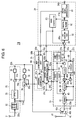
- Fig. 1 is a block diagram of a high-frequency receiver.
- high-frequency receiver 21 that receives a digital television broadcast signal.
- High-frequency receiver 21 includes matching device for an antenna 22, high-frequency receiving unit 23 that is connected to output terminal 22b of matching device for an antenna 22, demodulator 24 that is connected to output terminal 23b of high-frequency receiving unit 23 and demodulates a digital signal, and antennal control unit 25 that controls matching device for an antenna 22.
- Matching device for an antenna 22 has input terminal 22a that is connected to small antenna 31 with a length shorter than a quarter wavelength, and output terminal 22b. Between input terminal 22a and output terminal 22b, protection circuit 32 that protects back-stage electric circuits from electrical shock, such as static electricity from small antenna 31, matching device 33 that reduces tuning loss between input and output, antenna amplifying circuit 34 that amplifies a received signal, and attenuator 35 that uses resistors are connected in that order as viewed from input terminal 22a.
- protection circuit 32 that protects back-stage electric circuits from electrical shock, such as static electricity from small antenna 31
- matching device 33 that reduces tuning loss between input and output
- antenna amplifying circuit 34 that amplifies a received signal
- attenuator 35 that uses resistors
- a serial connector having electronic switch 36 that can select opening/closing and attenuator 37 that uses resistors is connected in parallel between input terminal 34a of antenna amplifying circuit 34 and output terminal 35b of attenuator 35.
- Matching device for an antenna 22 has antenna control terminal 22c, to which an antenna control signal is input.
- the antenna control signal input from antenna control terminal 22c is input to control input terminal 36a of electronic switch 36 and control input terminal 34a of antenna amplifying circuit 34.
- First terminal 40a of electronic switch 40 is connected to output terminal 22b of matching device for an antenna 22.
- High-frequency receiving unit 23 is designed to have input impedance of 75 ⁇ .
- output terminal 22b of matching device for an antenna 22 also has output impedance of 75 ⁇ to be tuned to input impedance of 75 ⁇ of high-frequency receiving unit 23. Further, a microstrip line with impedance of 75 ⁇ is provided between matching device for an antenna 22 and high-frequency receiving unit 23. Thus, it is possible to reduce tuning loss due to electrical connection.
- Second terminal 40b of electronic switch 40 is connected to external antenna 41.
- Common terminal 40c of electronic switch 40 is connected to input terminal 23a of high-frequency receiving unit 23.
- High-frequency receiving unit 23 has input terminal 23a and output terminal 23b. Between input terminal 23a and output terminal 23b, filter 42 that suppresses an interference signal, gain controllable amplifying circuit 43 having gain control input 43a, filter 44 that is connected to an output of amplifying circuit 43 and suppresses an interference signal, mixer 45 that is connected to first input terminal 45a, filter 46 that passes a frequency-converted output signal and suppresses an interference signal, and gain controllable amplifying circuit 47 having gain control input 47a are connected in that order as viewed from input terminal 23a.
- Second input terminal 45b of mixer 45 is connected to an output terminal of oscillator 48.
- An oscillation frequency of oscillator 48 is adjusted by a control voltage extracted from output terminal 49b of phase locked loop (PLL) circuit 49.
- Control data from input terminal 23c is input to input terminal 49a of PLL circuit 49.
- the control voltage extracted from output terminal 49b of PLL circuit 49 is input to tuning circuits of filters 42 and 44 to vary tuning frequencies of the filters.
- Filters 42 and 44 may be fixed filters having fixed tuning frequencies, not varying the tuning frequencies.
- An output signal of filter 46 is input to gain controllable amplifying circuit 47 having gain control input 47a.
- An output signal of amplifying circuit 47 is input to gain controller 56 to which an input signal is input and from which a gain control voltage is output.
- the gain control voltage is input to gain control input 47a of amplifying circuit 47.
- Demodulator 24 has input terminal 24a and output terminal 24b. Between input terminal 24a and output terminal 24b, gain controllable amplifying circuit 58 having gain control input 58a, A/D converter 59, digital filter 60, and digital demodulator 61 are connected in that order as viewed from input terminal 24a.
- An output signal extracted from digital filter 60 is input to gain controller 63 to which the input signal is input and from which the gain control voltage is output.
- the gain control voltage is input to gain control input terminal 58a of amplifying circuit 58.
- Antenna control unit 25 includes BER (Bit Error Ratio) determination unit 66, signal level determination unit 69, and antenna controller 67 having input terminals 67a and 67b to which output signals of both BER determination unit 66 and signal level determination unit 69 are respectively input.
- BER Bit Error Ratio
- the BER output from output terminal 61a of digital signal demodulator 61 is input to input terminal 66a of BER determination unit 66 through input terminal 25a of antenna control unit 25.
- Input terminal 66b of BER determination unit 66 is connected to BER input terminal 25b to which a BER reference value is input.
- a carrier-to-noise ratio (C/N) detector may be used to detect reception quality C/N value.
- Signal level determination unit 69 has input terminals 69a, 69b, 69c, and 69d.
- the gain control voltages output from gain controllers 56, 63, and 54 are input to input terminals 69a, 69b, and 69d, respectively.
- the gain control voltages are compared with individual reference voltages to determine their amplitudes.
- the referencevoltages maybeinput, for example, from input terminal 69c through reference voltage input terminal 25c of antenna control unit 25.
- An antenna control signal that controls matching device for an antenna 22 is input to switch control input 36a of electronic switch 36 and control input 34a of antenna amplifying circuit 34 based on determination signals output from BER determination unit 66 and signal level determination unit 69.
- high-frequency receiver 21 having the above-described configuration will be described with reference to Figs. 1 and 2 by way of an example where a high-frequency signal of a UHF band channel is received. It is assumed that output terminal 22b of matching device for an antenna 22 and input terminal 23a of high-frequency receiving unit 23 are connected to each other by electronic switch 40.
- the reception condition in addition to the relationship between the amplitudes of the signal levels of the digital and analog broadcast signals, the relationship between the amplitudes of the analog broadcast signals or the amplitudes of the digital broadcast signals can be exemplified. In this case, the same effects can also be obtained.
- Matching device for an antenna 22 can select one of an output signal extracted from antenna amplifying circuit 34 and an output signal extracted from matching device 33.
- antenna amplifying circuit 34 When an antenna control signal output from antenna controller 67 is input to matching device for an antenna 22, electronic switch 36 is opened (off state) and power is supplied to antenna amplifying circuit 34. That is, antenna amplifying circuit 34 is in an operation state and the connection to attenuator 37 is blocked.
- a received signal to small antenna 31 is input to matching device 33 through protection circuit 32.
- Matching device 33 is provided to suppress tuning loss between small antenna 31 and antenna amplifying circuit 34, and to suppress transmission loss of the received signal.
- the received signal to small antenna 31 is transmitted to antenna amplifying circuit 34 with suppressed transmission loss.
- Antenna amplifying circuit 34 amplifies the received signal.
- An output signal of antenna amplifying circuit 34 is input to attenuator 35.
- Attenuator 35 may have resistors, such that output impedance of matching device for an antenna 22 may have only a resistive component, with no a reactance component, and thus it may not depend on the magnitude of the frequency. For example, the magnitude is set to 75 ⁇ .
- an output signal of matching device 33 is output to output terminal 22b through electronic switch 36 and attenuator 37.
- Attenuator 37 may be an attenuator having resistors, such that output impedance of matching device for an antenna 22 may have only a resistive component, with no reactance component, and thus it may not depend on the magnitude of the frequency. For example, the magnitude is set to 75 ⁇ .
- matching device for an antenna 22 has a received channel gain on a UHF band of approximately 10 dB when loss in protection circuit 32 and matching device 33 is -1 dB, a gain in antenna amplifying circuit 34 is 15 dB, and loss in attenuator 37 is -4 dB.
- small antenna 31 Since small antenna 31 has a length shorter than a quarter wavelength, it has a gain lower than that of external antenna 41 by -10 dB. Thus, when external antenna 41 or small antenna 31 is used, almost the same input level is input to high-frequency receiving unit 23.
- the gain of matching device for an antenna 22 is output at a level lower by gain in antenna amplifying circuit 34 of 15 dB, since loss in protection circuit 32 and matching device 33 is -1 dB, loss in attenuator 37 is -4 dB, and gain in antenna amplifying circuit 34 is 0 dB.
- An output signal of matching device for an antenna 22 is input to filter 42 through input terminal 23a.
- Filter 42 suppresses an interference signal other than desired signal.
- An output signal of filter 42 is amplified by amplifying circuit 43 and input to filter 44. After filter 44 suppresses the interference signal other than desired signal, the desired signal is input to first input terminal 45a of mixer 45.
- An output signal of oscillator 48 controlled by PLL circuit 49 is input to second input terminal 45b.
- PLL control data is input to input terminal 49a of PLL circuit 49 through input terminal 23c.
- the oscillation frequency of oscillator 48 and tuning frequencies of filters 42 and 44 are controlled by the control voltage output from output terminal 49b of PLL circuit 49. With this circuit operation, the desired signal is selected among received signals.
- a desired signal for example, with an intermediate frequency of 8 MHz is output from output terminal 45c of mixer 45.
- the signal with intermediate frequency is input to filter 46, which suppresses the interference signal, and gain controller 54.
- a fixed BPF bandpass filter
- filter 46 is used as filter 46, thereby suppressing, for example, an interference signal close to the desired signal.
- Gain control voltage output from gain controller 54 is input to gain control input terminal 43a of amplifying circuit 43, which controls gain so that an output signal of mixer 45 can be constant.
- An output signal of filter 46 is amplified by amplifying circuit 47, is output from output terminal 23b of high-frequency receiving unit 23, and is input to gain controller 56 that outputs the gain control voltage.
- the gain control voltage is input to gain control input terminal 47a of amplifying circuit 47, and an output signal of amplifying circuit 47 is gain-controlled to have a constant level.
- the received signal input to input terminal 23a is frequency-converted by mixer 45 and gain-controlled by amplifying circuits 43 and 47, such that a signal output from output terminal 23b can have a constant level.
- An output signal of high-frequency receiving unit 23 is input to amplifying circuit 58 through output terminal 23b and input terminal 24a.
- a signal amplified by amplifying circuit 58 is input to A/D converter 59 that converts analog signals to digital signals.
- a digital signal output from A/D converter 59 is input to digital filter 60 that suppresses an interference signal.
- a digital signal output from digital filter 60 is input to digital signal demodulator 61.
- a TS (transport stream) signal is output from output terminal 24b of digital signal demodulator 61.
- An output signal of digital filter 60 is input to gain controller 63 that outputs the gain control voltage.
- the gain control voltage is input to gain control input terminal 58a of amplifying circuit 58.
- Amplifying circuit 58 controls the gain such that an input level to digital signal demodulator 61 can be constant.
- BER determination unit 66 compares a BER reference value, which is input through BER input terminal 25b, and BER, which is output from digital signal demodulator 61.
- a determination signal output from BER determination unit 66 is input to input terminal 67a of antenna controller 67.
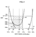
- Fig. 2 is a graph showing the relationship between BER and an input signal level to input terminal 22a of high-frequency receiver 21. It is assumed that the output signal from antenna amplifying circuit 34 is selected in matching device for an antenna 22.
- an input signal level having a reception level equal to or higher than -50 dBm is defined as a strong electric field area
- an input signal level having a reception level equal to or lower than -90 dBm is defined as a weak electric field area.
- Amplifying circuit 43 has a gain control range of 0 to -50 dBm as an input signal level at input terminal 22a.
- Amplifying circuit 47 has a gain control range of -50 to -90 dBm as an input signal level at input terminal 22a.
- Amplifying circuit 58 has a gain control range equal to or lower than -90 dBm as an input signal level at input terminal 22a.
- horizontal axis 101 indicates an input signal level from small antenna 31.
- reference numeral 101a indicates a weak signal level (-110 dBm) and reference numeral 101b indicates a strong signal level (-10 dBm).
- Vertical axis 102 indicates BER (Bit Error Ratio).
- BER 102a indicates an error-free state.
- BER 103 indicates a magnitude of 2 ⁇ 10 -4 .
- the reception quality i.e., C/N value, is regarded to be poor when BER is greater than 2 ⁇ 10 -4 .
- Characteristic curve 104 indicates BER when only a desired signal is received. It can be seen from characteristic curve 104 that BER becomes 102b at input signal level 101c (-90 dBm) and BER is deteriorated at input signal level 101a (-110 dBm). The deterioration results from a noise index of high-frequency receiver 21 and deteriorated C/N of a received signal.
- BER is deteriorated at an input signal level greater than signal level 101d (-20 dBm) since signal distortion occurs due to a high-level desired signal input to antenna amplifying circuit 34andhigh-frequencyreceivingunit23.
- signal level 101d 20 dBm
- an effect by distortion may be serious.
- Characteristic curve 105 indicates BER when a desired signal and an interference signal that is about 40 dB greater than the desired signal are received. BER becomes 102c at input signal level 101c (-90 dBm), which is almost the same as characteristic curve 104.
- BER 102d indicates that BER is deteriorated, and is close to BER 103 (2 ⁇ 10 -4 ) of a reference value indicating that C/N value is determined to be poor.
- BER is 102e at input signal level 101f (-65 dBm), which is better than BER 102d at input signal level 101e (-50 dBm). This is because the interference signal is reduced from -10 dBm to -25 dBm, even though the desired signal is reduced from -50 dBm to -75 dBm.
- a gain difference of matching device for an antenna 22 between the operation state and non-operation state of antenna amplifying circuit 34 is preferably, for example, equal to or greater than 15 dB.
- matching device for an antenna 22 has a gain of 10 dB in a case where an output signal from antenna amplifying circuit 34 is selected.
- a signal that is 10 dB greater than an input level to antenna amplifying circuit 34 is input to an input terminal of high-frequency receiving unit 23.
- the input terminal of high-frequency receiving unit 23 is connected to filters 42 and 44 that suppress interference signals.
- signal distortion easily occurs in matching device for an antenna 22 compared to high-frequency receiving unit 23, which causes BER to be deteriorated.
- signal distortion occurs in antenna amplifying circuit 34 of matching device for an antenna 22 when a signal equal to or greater than -10 dBm is input.
- BER determination unit 66 compares the magnitude of the received BER with the BER reference value (2 ⁇ 10 -4 ). When the received BER is greater than the BER reference value (2 ⁇ 10 -4 ), electronic switch 36 of matching device for an antenna 22 is closed by an antenna control signal output from antenna controller 67 and simultaneously power supply to antenna amplifying circuit 34 stops, such that input signal level 101e (-50 dBm) can be set to input signal level 101f (-65 dBm) .
- antenna amplifying circuit 34 When a weak electric field level less than input signal level 101c (-90 dBm) is received, electronic switch 36 may be opened and simultaneously antenna amplifying circuit 34 may be in the operation state.
- BER determination unit 66 determines the magnitude of the received BER, it is difficult to determine whether the BER is deteriorated due to the interference signal or weak electric field.
- Amplifying circuit 43 has a gain control range of 0 to -50 dBm as an input signal level at input terminal 23a.
- amplifying circuit 47 has a gain control range of (-50 dBm +V1) to (-90 dBm +V1). Accordingly, it is possible to provide high-frequency receiver 21 that optimizes the input signal level and suppresses noise and distortion.
- the operation of high-frequency receiver 21 will be described according to the amplitudes of the desired signal and the interference signal in high-frequency receiver 21.
- the reception condition is that small antenna 31 is used, and digital broadcast is received as a desired signal of -50 dBm and analog broadcast is received as an interference signal of -10 dBm at input terminal 22a.
- the interference signal is suppressed, for example, by 15 dB by filter 42.
- the suppressed interference signal of -25 dBm is input to .amplifying circuit 43.
- Amplifying circuit 43 executes a gain control of 0 dBm to -50 dBm as an input signal level at input terminal 23a.
- amplifying circuit 43 executes a gain control of 25 dBm that is obtained by subtracting a gain signal of -50 dBm from the interference signal of -25 dBm.
- the interference signal input to amplifying circuit 47 has a level of (-50 dBm + V1 - Vs), in which -50 dBm is obtained by subtracting a gain control of 25 dBm from the interference signal of -25 dBm, adding the gain V1, and subtracting a suppressed amount Vs for the interference signal in filter 46.
- -50 dBm is obtained by subtracting a gain control of 25 dBm from the interference signal of -25 dBm, adding the gain V1, and subtracting a suppressed amount Vs for the interference signal in filter 46.
- a SAW filter is used as filter 46, it is possible to make the suppressed amount Vs equal to or greater than 40 dB.
- the desired signal output from filter 46 has a level of (-75 dBm + V1), in which -75 dBm is obtained by subtracting a gain control of 25 dBm from the desired signal of -50 dBm, and adding the gain V1. That is, since the interference signal is suppressed by filter 46 by 25 dB from the desired signal, signal distortion rarely occurs in back-stage circuits.
- the desired signal (-75 dBm + V1 output from filter 46 is input to amplifying circuit 47.
- Amplifying circuit 47 has a gain control range of (-50 dBm + V1) to (-90 dBm + V1).
- amplifying circuit 47 executes a gain control of -15 dBm that is obtained by subtracting the lower limit (-90 dBm + V1) of the gain control range from the desired signal of (-75 dBm + V1).
- amplifying circuit 47 executes a gain control of -15 dBm according to the desired signal. That is, a gain control voltage at gain control input 47a varies depending on the magnitude of the desired signal.
- the magnitude of desired signal varies depending on the magnitude of the interference signal. As the interference signal becomes strong, the gain control becomes large in amplifying circuit 43. As a result, since the desired signal input to amplifying circuit 47 becomes weak, amplifying circuit 47 is controlled such that the gain becomes larger.
- signal level determination unit 69 is used to compare the gain control voltages of gain controllers 54 and 56 with the upper limit and lower limit of the reference voltage, thereby detecting the amplitude of interference signal level.
- the upper and lower limits of the reference voltage of signal level determination unit 69 can be input through reference voltage input terminal 25c. Thus, it is possible to easily set the optimum value through an external terminal.
- a determination signal from signal level determination unit 69 is input to input terminal 67b of antenna controller 67.
- antenna control signal output from antenna controller 67 power supply to antenna amplifying circuit 34 stops and simultaneously electronic switch 36 is closed.
- the interference signal since it is possible to reduce the interference signal, for example, by 15 dB, it is possible to prevent distortion from occurring in matching device for an antenna 22 and to suppress distortion from occurring in amplifying circuit 43 and mixer 45, thereby improving interference-resistant characteristics of high-frequency receiver 21.
- the desired signal is changed from -50 dBm to -75 dBm that is a relatively low level. As shown in characteristic curve 105 of Fig. 2, the BER is not deteriorated.
- a signal with a constant level which is gain-controlled by amplifying circuit 43 having a gain control range of, for example, 0 dBm to -50 dBm, is input to amplifying circuit 47.
- gain control voltage of amplifying circuit 47 has a minimum gain, the gain control voltage of gain controller 56 remains unchanged.
- a determination signal from signal level determination unit 69 is input to input terminal 67b of antenna controller 67.
- antenna control signal output from antenna controller 67 power supply to antenna amplifying circuit 34 stops and simultaneously electronic switch 36 is closed.
- a desired signal is received in a weak electric field area (equal to or less than -90 dBm)
- amplifying circuits 43 and 47 are controlled so as to obtain maximum gains, and a signal with a constant level, which is gain-controlled by amplifying circuit 58 having a gain control range equal to or less than -90 dBm, is input to A/D converter 59.
- the gain control voltage of gain controller 63 is changed.
- an output signal of antenna amplifying circuit 34 is output from output terminal 22b, and the input level to high-frequency receiving unit 23 can be raised by 15 dB compared to a case where the output signal of matching device 33 is output from output terminal 22b. Accordingly, it is possible to improve reception sensitivity with respect to a weal signal level.
- matching device for an antenna 22 operates with a gain close to a maximum value by an antenna control signal from antenna controller 67. Thus, it is possible to output a signal with suppressed noise from high-frequency receiving unit 23.
- high-frequency receiver 21 having both an interference characteristic in a strong electric field area and reception sensitivity in a weak electric field area by switching the operation state of matching device for an antenna 22 by the antenna control signal.
- the determination signal from BER determination unit 66 is input to antenna controller 67.
- BER determination unit 66 compares the magnitude of the received BER with the BER reference value (2 ⁇ 10 -4 ) .
- antenna controller 67 performs determination using the determination signals of signal level determination unit 69 and BER determination unit 66, accuracy in determination increases.
- the gain control ranges of individual amplifying circuits 43, 47, and 58 of high-frequency receiving unit 23 may be reset based on the interference characteristic and reception sensitivity. Only one of gain controllers 54, 56, and 63 may not be sufficient to detect the magnitudes of the desired signal and interference signal. In this case, some of gain controllers 54, 56, and 63 may be used to detect the magnitudes of the desired signal and interference signal.
- the gain control voltages are configured to correspond to variable reception conditions. Accordingly, it is possible to select optimum reception performance in a short time to correspond to a case where a signal is received in a strong electric field area where there is a high possibility that a strong interference signal is received or a case where a signal is received in a weak electric field area. Accordingly, this is desirable when TV signals are received during movement.
- a D/A converter (not shown) may be provided between gain controllers 54, 56, and 63 and the signal level determination unit, and the digital values output from the D/A converter may be signal-processed through I2C (Inter Integrated Circuit) bus lines. In this case, since signal processing can be performed through common I2C bus lines, wiring is simplified.
- I2C Inter Integrated Circuit
- C/N values from digital signal demodulator 61 may be input to C/N determination unit 70 (not shown).
- the supply and stop of power to antenna amplifying circuit 34 and the opening and closing of electronic switch 36 should be controlled such that the signals input to high-frequency receiving unit 23 are continuous. Discontinuous signals result in unstable images or discontinuous voices.
- direct-conversion mixer may be used. That is, two mixers for I and Q signals are used as mixer 45, and the oscillation signals that are output from oscillator 48 and have a phase difference of 90° to each other are input to the mixers for I and Q signals.
- frequencies after direct-conversion become low-frequency signals of the I and Q signals. That is, since it is possible to perform signal processing to low frequencies, integration is facilitated, and interference with other signals is difficult to occur.
- an analog signal demodulator (not shown) may be used, instead of digital signal demodulator 24, and an S/N detection signal from analog signal demodulator 24c may be used. Accordingly, it is possible to obtain the same effect by inputting the S/N detection signal to the S/N determination unit, instead of BER determination unit 66, and inputting a determination value from the S/N determination unit to antenna controller 67.
- matching device for an antenna 22 may be high-frequency shielded.
- a serial circuit of electronic switch 36 and attenuator 37 is incorporated in matching device for an antenna 22, it is possible to protect matching device for an antenna 22 from external unnecessary radiation signals with high frequencies.
- Matching device for an antenna 22 is connected to input terminal 23a of high-frequency receiving unit 23 that receives TV broadcast signals.
- Matching device for an antenna 22 includes first input terminal 22a to which the received signal input through antenna 31 is input, and matching device 33 that is connected to first input terminal 22a and suppresses tuning loss.
- Matching device for an antenna 22 further includes antenna amplifying circuit 34 that is connected to output terminal 33b of matching device 33 and amplifies received signals, and first output terminal 22b from which an output signal of antenna amplifying circuit 34 is extracted.
- Matching device for an antenna 22 further includes first electronic switch 36 that is connected in parallel to input terminal 34a and output terminal 34b of antenna amplifying circuit 34. Further, antenna control terminal 22c that controls first electronic switch 36 and antenna amplifying circuit 34 is provided.
- matching device for an antenna 22 opens first electronic switch 36 and operates antenna amplifying circuit 34, for example, in a first electric field area, i.e. , in a weak electric field area.
- Matching device for an antenna 22 closes first electronic switch 36 and stops the operation of the antenna amplifying circuit 34, for example, in a second electric field area, i.e. , in a strong electric field area.
- a second embodiment describes matching device 33 that is used in matching device for an antenna 22 with reference to Figs. 3a, 3b, and 3c.
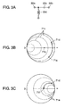
- Fig. 3a is a representative circuit diagram of matching device 33.
- Matching device 33 suppresses tuning loss between small antenna 31 and antenna amplifying circuit 34, and reduces transmission loss of received signals.
- Terminals 33a and 33b are input and output terminals of matching device 33, respectively.
- Fig. 3b shows impedance on an admittance chart.
- Small antenna 31 receives UHF and VHF bands. Since a portable small antenna is not easy to have a length of a quarter wavelength, it has input impedance 71a with large resistance in a VHF band, particularly. It is assumed that there is no effect of protection circuit 32 on impedance.
- Antenna amplifying circuit 34 has input impedance 71b close to, for example, 150 ⁇ .
- impedance 71a of small antenna 31 is rotated in a counterclockwise direction along constant conductance circle 71c by inductor 33d (see Fig. 3a) connected in parallel. As a result, it moves to impedance 71d.
- Fig. 3c shows impedance on a Smith chart. Impedance 71d is rotated in a counterclockwise direction along constant resistance circle 71e by capacitor 33c connected in series. As a result, it moves to impedance 71f.
- inductor 33d and capacitor 33c By using inductor 33d and capacitor 33c to move impedance, it is possible to make impedance on small antenna 31 seen from output terminal 33b close to input impedance of antenna amplifying circuit 34. That is, it is possible to secure tuning between small antenna 31 and antenna amplifying circuit 34. Thus, signals received by small antenna 31 are input to antenna amplifying circuit 34 with low transmission loss.
- inductor 33d and capacitor 33c of matching device 33 can be selected to have optimum values by means of electronic switch 36, it is possible to secure optimum tuning between small antenna 31 and antenna amplifying circuit 34 even though received bands are changed.
- a third embodiment of the invention describes attenuators 35 and 37 that are used in matching device for an antenna 22 with reference to Figs. 4 and 5.
- Fig. 4 is a circuit diagram of attenuator 35 connected between antenna amplifying circuit 34 and output terminal 22b. Terminals 35a and 35b are input and output terminals of attenuator 35, respectively.
- attenuator 35 is constructed of pi-shaped attenuator consisting of resistors 35c, 35d, and 35e.
- output impedance of matching device for an antenna 22 may have only a resistive component, for example, 75 ⁇ , with no reactance component without depending on magnitude of frequency.
- tuning loss caused by coupling with high-frequency receiving unit 23 may be fixed within an allowable range. That is, it is possible to maintain constant reception sensitivity between channels.
- Attenuator 35 has an attenuation of 4 dB. Attenuator 35 can be set to have an optimum attenuation by selecting appropriate resistors.
- Fig. 5 is a circuit diagram of attenuator 37 connected between electronic switch 36 and output terminal 22b. Terminals 37a and 37b are input and output terminals of attenuator 37, respectively.
- output impedance of matching device for an antenna 22 may have only a resistive component, for example, 75 ⁇ , with no reactance component without depending on magnitude of frequency.
- tuning loss caused by coupling with high-frequency receiving unit 23 may be fixed within an allowable range. That is, it is possible to maintain constant reception sensitivity between channels.
- an attenuation can be set to 4 dB.
- attenuator 37 can be set to have an optimum attenuation by selecting appropriate resistors.
- Individual attenuators 35 and 37 may be constructed of T-shaped resistors. Further, a circuit with no resistor 35d or a circuit with no resistor 37d may be used.
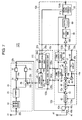
- High-frequency receiver 74 according to a fourth embodiment of the invention will be described with reference to Fig. 6.
- matching device for an antenna 22 includes electronic switch 36 and attenuator 37.
- electronic switch 36 and attenuator 37 are provided outside matching device for an antenna 75, and electronic switch 36 is connected to the input terminal of matching device 33, rather than the input terminal of antenna amplifying circuit 34.
- Fig. 6 the same elements as those shown in Fig. 1 are denoted by the same reference numerals and the detailed descriptions thereof will be omitted.
- the input terminal of matching device 33 is connected to output terminal 75a.
- Electronic switch 36, matching device 76, and attenuator 37 are connected between output terminal 75a and output terminal 22b in that order as viewed from output terminal 75a.
- An antenna control signal output from antenna controller 67 is input to control input terminal 36a of electronic switch 36 and simultaneously is input to control input terminal 34a of antenna amplifying circuit 34 through input terminal 75b.
- high-frequency receiver 74 The operation of high-frequency receiver 74 is basically the same as that described in Fig. 1 and the detailed description thereof will be omitted.
- electronic switch 36, matching device 76, and attenuator 37 are connected between output terminal 75a and output terminal 22b of matching device for an antenna 75. That is, since they are provided outside matching device for an antenna 75, it is possible to reduce the size of matching device for an antenna 75 and simultaneously to provide matching device for an antenna 75 adjacent to small antenna 31. Accordingly, small antenna 31 and matching device for an antenna 75 can be formed as a single body.
- Matching device 76 is provided between output terminal 75a and output terminal 22b and outside matching device for an antenna 75.
- matching device 76 can have a tuning circuit with a lot of elements.
- it is possible to secure tuning between small antenna 31 and high-frequency receiving unit 23. Accordingly, it is possible to prevent a change in tuning loss by the received channels.
- Output terminal 75a of matching device for an antenna 75 may be connected to the input terminal of antenna amplifying circuit 34, instead of the input terminal of matching device 33.
- antenna amplifying circuit 34 has input impedance of about 75 ⁇
- matching device 33 has output impedance of 75 ⁇ .
- High-frequency receiver 121 will be described with reference to Fig. 7.
- amplifying circuits 47 and 58 are gain-controlled by gain controllers 56 and 63, respectively.
- the gain control voltages from gain controllers 54, 56, and 63 are input to input terminals 69d, 69a, and 69b of signal level determination unit 69, respectively.
- gain controller 63 is not provided, but amplifying circuit 158 having constant amplification degree is used. That is, the first to fourth embodiments have used amplifying circuit 58 having a variable amplification degree, as shown in Figs. 1 and 6, while the fifth embodiment uses amplifying circuit 158 having a fixed amplification degree.
- An output signal of digital filter 60 other than an output signal of amplifying circuit 47 is input to an input terminal of gain controller 56.
- Gain control voltages from gain controllers 54 and 56 are input to input terminals 169d and 169a of signal level determination unit 169, respectively.
- High-frequency receiver 121 includes matching device for an antenna 22 that is connected to small antenna 31, high-frequency receiving unit 123 that is connected to output terminal 22b of matching device for an antenna 22, demodulator 124 that is connected to output terminal 123b of high-frequency receiving unit 123 and has output terminal 124b, and antenna control unit 125 that receives gain control voltages output from gain controllers 54 and 56 of high-frequency receiving unit 123, respectively, and BER signal output from demodulator 124 to control electronic switch 36.
- the operation of high-frequency receiver 121 is basically the same as that described in Fig. 1 and a simplified description thereof will be given.
- a received signal input to input terminal 123a is frequency-converted by mixer 45 and simultaneously is gain-controlled in amplifying circuits 43 and 47 such that signal levels output from output terminal 123b can be constant.
- signal level determination unit 169 is used to compare gain control voltages of gain controllers 54 and 56 with upper and lower limits of a reference voltage of each of gain controllers 54 and 56, thereby detecting the level of the interference signal.
- a determination signal from signal level determination unit 169 is input to input terminal 67b of antenna controller 67.
- antenna control signal output from antenna controller 67 power supply to antenna amplifying circuit 34 stops and simultaneously electronic switch 36 is closed.
- the interference signal can be reduced, for example, by 15 dB, it is possible to prevent distortion from occurring in matching device for an antenna 22 and to prevent distortion from occurring in amplifying circuit 43 and mixer 45, thereby improving interference-resistant characteristics of high-frequency receiver 121.
- a desired signal is reduced from -50 dBm to -75 dBm, and BER is not deteriorated, as shown in characteristic curve 105 of Fig. 2.
- a determination signal from signal level determination unit 169 is input to input terminal 67b of antenna controller 67.
- antenna control signal output from antenna controller 67 power supply to antenna amplifying circuit 34 stops and simultaneously electronic switch 36 is closed.
- the desired signal can be reduced by about 15 dB, it is possible to suppress distortion from occurring in amplifying circuit 43 and mixer 45 and to improve interference-resistant characteristics of high-frequency receiver 121.
- a case where a desired signal is received in a weak electric field area (equal to or less than -90 dBm) will be described.
- amplifying circuit 43 is controlled so as to obtain a maximum gain, and a signal with a constant level that is gain-controlled by amplifying circuit 47 is input to A/D converter 59.
- the gain control voltage of gain controller 56 is changed.
- an output signal of antenna amplifying circuit 34 is output from output terminal 22b.
- An input signal level input to high-frequency receiving unit 123 can be raised by about 15 dB compared to a case where an output signal of matching device 33 is output from output terminal 22b. As a result, reception sensitivity with respect to a weak signal level is improved.
- matching device for an antenna 22 When a signal is received in a weak electric field area, matching device for an antenna 22 operates with a gain close to a maximum value by an antenna control signal from antenna controller 67. Thus, it is possible to output a signal with noise suppressed from high-frequency receiving unit 123.
- a determination signal from BER determination unit 66 is input to antenna controller 67.
- BER determination unit 66 compares the magnitude of the received BER with the BER reference value (2 ⁇ 10 -4 ), and determines whether or not the magnitude is appropriate.
- antenna controller 67 performs determination using the determination signals of signal level determination unit 169 and BER determination unit 66, accuracy in determination increases.
- Gain control ranges of individual amplifying circuits 43, 47, and 158 of high-frequency receiving unit 123 may be reset based on the interference characteristic and reception sensitivity. Only one of gain controllers 54 and 56 may not be sufficient to detect the magnitudes of the desired signal and interference signal. In this case, gain controllers 54 and 46 may be used to detect the magnitudes of the desired signal and interference signal.
- the gain control voltages are configured to correspond to variable reception conditions. Accordingly, it is possible to select optimum reception performance in a short time to correspond to a case where a signal is received in a strong electric field area where a strong interference signal exists or a case where a signal is received in a weak electric field area. Accordingly, this is desirable when TV signals are received during movement.
- direct-conversion mixer may be used. That is, two mixers for I and Q signals are used as mixer 45, and the oscillation signals that are output from oscillator 48 and have a phase difference of 90° to each other are input to the mixers for I and Q signals.
- frequencies after direct-conversion become low-frequency signals of the I and Q signals. That is, since it is possible to perform signal processing to low frequencies, integration is facilitated, and interference with other signals is suppressed.
- an analog signal demodulator (not shown) may be used, instead of digital signal demodulator 124, and an S/N detection signal from the analog signal demodulator may be used. Accordingly, it is possible to obtain the same effect by inputting the S/N detection signal to the S/N determination unit, instead of BER determination unit 66, and inputting a determination value from the S/N determination unit to antenna controller 67.
- a matching device for an antenna and a high-frequency receiver using the matching device for an antenna according to the invention can improve both an interference characteristic in a strong electric field area and reception sensitivity in a weak electric field area.
- the matching device for an antenna and high-frequency receiver are useful when signals are received during movement in a strong electric field area where a strong interference signal exists.
Landscapes
- Engineering & Computer Science (AREA)
- Computer Networks & Wireless Communication (AREA)
- Signal Processing (AREA)
- Input Circuits Of Receivers And Coupling Of Receivers And Audio Equipment (AREA)
Applications Claiming Priority (2)
| Application Number | Priority Date | Filing Date | Title |
|---|---|---|---|
| JP2005228199 | 2005-08-05 | ||
| JP2006123220A JP2007068143A (ja) | 2005-08-05 | 2006-04-27 | アンテナ整合器とこれを用いた高周波受信装置 |
Publications (2)
| Publication Number | Publication Date |
|---|---|
| EP1750375A2 true EP1750375A2 (de) | 2007-02-07 |
| EP1750375A3 EP1750375A3 (de) | 2009-08-05 |
Family
ID=37054672
Family Applications (1)
| Application Number | Title | Priority Date | Filing Date |
|---|---|---|---|
| EP06118427A Withdrawn EP1750375A3 (de) | 2005-08-05 | 2006-08-04 | HF-Empfänger und Anpassungsvorrichtung für den Empfänger |
Country Status (3)
| Country | Link |
|---|---|
| US (1) | US20070030062A1 (de) |
| EP (1) | EP1750375A3 (de) |
| JP (1) | JP2007068143A (de) |
Cited By (1)
| Publication number | Priority date | Publication date | Assignee | Title |
|---|---|---|---|---|
| DE102008011872A1 (de) | 2008-02-27 | 2009-09-10 | Technisat Digital Gmbh | Verfahren zur Anpassung einer Rundfunkempfangsantenne an eine Empfangssituation |
Families Citing this family (3)
| Publication number | Priority date | Publication date | Assignee | Title |
|---|---|---|---|---|
| JP4514801B2 (ja) | 2008-01-22 | 2010-07-28 | シャープ株式会社 | 放送受信装置 |
| US11283476B2 (en) * | 2019-07-09 | 2022-03-22 | Raytheon Bbn Technologies Corp. | System and method for cancelling strong signals from combined weak and strong signals in communications systems |
| CN111179804B (zh) * | 2020-01-13 | 2023-04-18 | 合肥鑫晟光电科技有限公司 | 一种时序控制器、显示装置、信号调整方法 |
Citations (1)
| Publication number | Priority date | Publication date | Assignee | Title |
|---|---|---|---|---|
| JP2005057642A (ja) | 2003-08-07 | 2005-03-03 | Matsushita Electric Ind Co Ltd | 携帯受信装置とこれに用いる分波器 |
Family Cites Families (16)
| Publication number | Priority date | Publication date | Assignee | Title |
|---|---|---|---|---|
| DE3821716A1 (de) * | 1988-06-28 | 1990-01-04 | Telefunken Electronic Gmbh | Fernsehtuner mit einer bandfilterschaltung |
| KR920001946A (ko) * | 1990-06-21 | 1992-01-30 | 강진구 | 텔레비젼 신호 수신 튜닝방식 및 회로 |
| DE4332161A1 (de) * | 1993-09-22 | 1995-03-23 | Thomson Brandt Gmbh | Hochfrequenzempfänger |
| US5722061A (en) * | 1994-12-16 | 1998-02-24 | Qualcomm Incorporated | Method and apparatus for increasing receiver immunity to interference |
| US6009129A (en) * | 1997-02-28 | 1999-12-28 | Nokia Mobile Phones | Device and method for detection and reduction of intermodulation distortion |
| US6498926B1 (en) * | 1997-12-09 | 2002-12-24 | Qualcomm Incorporated | Programmable linear receiver having a variable IIP3 point |
| JP4042328B2 (ja) * | 2001-01-16 | 2008-02-06 | 松下電器産業株式会社 | 高周波信号受信装置 |
| JP3713206B2 (ja) * | 2001-01-23 | 2005-11-09 | 株式会社ケンウッド | 自動利得制御回路 |
| JP2003051727A (ja) * | 2001-08-06 | 2003-02-21 | Clarion Co Ltd | 高周波増幅回路 |
| US20040041945A1 (en) * | 2001-09-25 | 2004-03-04 | Pugel Michael Anthony | Apparatus and method for optimizing the level of rf signals |
| JP2003243512A (ja) * | 2002-02-14 | 2003-08-29 | Hitachi Ltd | 静電破壊保護回路 |
| JP2005184646A (ja) * | 2003-12-22 | 2005-07-07 | Nissan Motor Co Ltd | 受信回路及び受信方法 |
| JP4301007B2 (ja) * | 2004-01-08 | 2009-07-22 | ミツミ電機株式会社 | 分配器及びそれを用いた放送信号受信システム |
| JP2005278122A (ja) * | 2004-03-26 | 2005-10-06 | Mitsubishi Electric Corp | 受信機 |
| JP2005311775A (ja) * | 2004-04-22 | 2005-11-04 | Mitsubishi Electric Corp | 受信機 |
| JP4120650B2 (ja) * | 2004-08-03 | 2008-07-16 | カシオ計算機株式会社 | 復調回路及び復調方法 |
-
2006
- 2006-04-27 JP JP2006123220A patent/JP2007068143A/ja active Pending
- 2006-08-04 EP EP06118427A patent/EP1750375A3/de not_active Withdrawn
- 2006-08-07 US US11/499,944 patent/US20070030062A1/en not_active Abandoned
Patent Citations (1)
| Publication number | Priority date | Publication date | Assignee | Title |
|---|---|---|---|---|
| JP2005057642A (ja) | 2003-08-07 | 2005-03-03 | Matsushita Electric Ind Co Ltd | 携帯受信装置とこれに用いる分波器 |
Cited By (1)
| Publication number | Priority date | Publication date | Assignee | Title |
|---|---|---|---|---|
| DE102008011872A1 (de) | 2008-02-27 | 2009-09-10 | Technisat Digital Gmbh | Verfahren zur Anpassung einer Rundfunkempfangsantenne an eine Empfangssituation |
Also Published As
| Publication number | Publication date |
|---|---|
| US20070030062A1 (en) | 2007-02-08 |
| EP1750375A3 (de) | 2009-08-05 |
| JP2007068143A (ja) | 2007-03-15 |
Similar Documents
| Publication | Publication Date | Title |
|---|---|---|
| JP3906792B2 (ja) | 高周波信号受信装置とその製造方法 | |
| US7546107B2 (en) | Apparatus and method for interference canceller in a high frequency receiver and transmitter | |
| US4592093A (en) | Super high frequency receiver | |
| US7362178B2 (en) | Wide dynamic range amplifier gain control | |
| US5369792A (en) | AGC circuit of FM front-end portion for controlling bandwidth detection sensitivity | |
| KR0160687B1 (ko) | 저잡음 증폭기를 갖는 영상신호 수신상치 | |
| EP1760879B1 (de) | Hochfrequenzempfänger | |
| US20090111410A1 (en) | FM receiver | |
| EP1750375A2 (de) | HF-Empfänger und Anpassungsvorrichtung für den Empfänger | |
| US9793934B2 (en) | Wireless receiver | |
| JP3626350B2 (ja) | 受信装置 | |
| JP2006217127A (ja) | 受信装置 | |
| JP4135746B2 (ja) | 高周波信号受信装置 | |
| KR20070017076A (ko) | 안테나 정합기 및 이것을 사용한 고주파 수신 장치 | |
| JP2005510933A (ja) | チューナの入力における信号強度を判定する方法 | |
| JP2005167860A (ja) | デジタルテレビ放送受信モジュール | |
| JPH06291688A (ja) | 受信機 | |
| JP3174230B2 (ja) | ラジオ受信機 | |
| JP3208167B2 (ja) | 複合型音響機器 | |
| JP2010147975A (ja) | 高周波受信装置 | |
| JP2005159591A (ja) | 放送受信装置 | |
| JP2011004046A (ja) | 放送受信装置および携帯端末機 | |
| JP2003283940A (ja) | Bsデジタルチューナー | |
| JPH04354210A (ja) | 通信装置の受信回路 | |
| KR20080049930A (ko) | 튜너 |
Legal Events
| Date | Code | Title | Description |
|---|---|---|---|
| PUAI | Public reference made under article 153(3) epc to a published international application that has entered the european phase |
Free format text: ORIGINAL CODE: 0009012 |
|
| AK | Designated contracting states |
Kind code of ref document: A2 Designated state(s): AT BE BG CH CY CZ DE DK EE ES FI FR GB GR HU IE IS IT LI LT LU LV MC NL PL PT RO SE SI SK TR |
|
| AX | Request for extension of the european patent |
Extension state: AL BA HR MK YU |
|
| RAP1 | Party data changed (applicant data changed or rights of an application transferred) |
Owner name: PANASONIC CORPORATION |
|
| PUAL | Search report despatched |
Free format text: ORIGINAL CODE: 0009013 |
|
| AK | Designated contracting states |
Kind code of ref document: A3 Designated state(s): AT BE BG CH CY CZ DE DK EE ES FI FR GB GR HU IE IS IT LI LT LU LV MC NL PL PT RO SE SI SK TR |
|
| AX | Request for extension of the european patent |
Extension state: AL BA HR MK RS |
|
| RIC1 | Information provided on ipc code assigned before grant |
Ipc: H04B 1/10 20060101ALI20090630BHEP Ipc: H04B 1/18 20060101AFI20061009BHEP |
|
| AKX | Designation fees paid | ||
| REG | Reference to a national code |
Ref country code: DE Ref legal event code: 8566 |
|
| STAA | Information on the status of an ep patent application or granted ep patent |
Free format text: STATUS: THE APPLICATION IS DEEMED TO BE WITHDRAWN |
|
| 18D | Application deemed to be withdrawn |
Effective date: 20100206 |