EP1753031B1 - Dispositif de logique quantique et circuit logique par dispositif de logique quantique - Google Patents
Dispositif de logique quantique et circuit logique par dispositif de logique quantique Download PDFInfo
- Publication number
- EP1753031B1 EP1753031B1 EP05743368.2A EP05743368A EP1753031B1 EP 1753031 B1 EP1753031 B1 EP 1753031B1 EP 05743368 A EP05743368 A EP 05743368A EP 1753031 B1 EP1753031 B1 EP 1753031B1
- Authority
- EP
- European Patent Office
- Prior art keywords
- quantum
- area
- areas
- logic
- quantum structure
- Prior art date
- Legal status (The legal status is an assumption and is not a legal conclusion. Google has not performed a legal analysis and makes no representation as to the accuracy of the status listed.)
- Expired - Lifetime
Links
Images




Classifications
-
- H—ELECTRICITY
- H10—SEMICONDUCTOR DEVICES; ELECTRIC SOLID-STATE DEVICES NOT OTHERWISE PROVIDED FOR
- H10D—INORGANIC ELECTRIC SEMICONDUCTOR DEVICES
- H10D62/00—Semiconductor bodies, or regions thereof, of devices having potential barriers
- H10D62/10—Shapes, relative sizes or dispositions of the regions of the semiconductor bodies; Shapes of the semiconductor bodies
-
- H—ELECTRICITY
- H10—SEMICONDUCTOR DEVICES; ELECTRIC SOLID-STATE DEVICES NOT OTHERWISE PROVIDED FOR
- H10D—INORGANIC ELECTRIC SEMICONDUCTOR DEVICES
- H10D30/00—Field-effect transistors [FET]
-
- H—ELECTRICITY
- H10—SEMICONDUCTOR DEVICES; ELECTRIC SOLID-STATE DEVICES NOT OTHERWISE PROVIDED FOR
- H10D—INORGANIC ELECTRIC SEMICONDUCTOR DEVICES
- H10D48/00—Individual devices not covered by groups H10D1/00 - H10D44/00
- H10D48/30—Devices controlled by electric currents or voltages
-
- H—ELECTRICITY
- H10—SEMICONDUCTOR DEVICES; ELECTRIC SOLID-STATE DEVICES NOT OTHERWISE PROVIDED FOR
- H10D—INORGANIC ELECTRIC SEMICONDUCTOR DEVICES
- H10D8/00—Diodes
- H10D8/70—Tunnel-effect diodes
-
- Y—GENERAL TAGGING OF NEW TECHNOLOGICAL DEVELOPMENTS; GENERAL TAGGING OF CROSS-SECTIONAL TECHNOLOGIES SPANNING OVER SEVERAL SECTIONS OF THE IPC; TECHNICAL SUBJECTS COVERED BY FORMER USPC CROSS-REFERENCE ART COLLECTIONS [XRACs] AND DIGESTS
- Y10—TECHNICAL SUBJECTS COVERED BY FORMER USPC
- Y10S—TECHNICAL SUBJECTS COVERED BY FORMER USPC CROSS-REFERENCE ART COLLECTIONS [XRACs] AND DIGESTS
- Y10S977/00—Nanotechnology
- Y10S977/70—Nanostructure
- Y10S977/762—Nanowire or quantum wire, i.e. axially elongated structure having two dimensions of 100 nm or less
-
- Y—GENERAL TAGGING OF NEW TECHNOLOGICAL DEVELOPMENTS; GENERAL TAGGING OF CROSS-SECTIONAL TECHNOLOGIES SPANNING OVER SEVERAL SECTIONS OF THE IPC; TECHNICAL SUBJECTS COVERED BY FORMER USPC CROSS-REFERENCE ART COLLECTIONS [XRACs] AND DIGESTS
- Y10—TECHNICAL SUBJECTS COVERED BY FORMER USPC
- Y10S—TECHNICAL SUBJECTS COVERED BY FORMER USPC CROSS-REFERENCE ART COLLECTIONS [XRACs] AND DIGESTS
- Y10S977/00—Nanotechnology
- Y10S977/70—Nanostructure
- Y10S977/773—Nanoparticle, i.e. structure having three dimensions of 100 nm or less
- Y10S977/774—Exhibiting three-dimensional carrier confinement, e.g. quantum dots
Definitions
- the present invention relates to a quantum device, a quantum logic device, a method of driving the quantum logic device, and a logic circuit. Particularly the present invention relates to a technique effectively used for a quantum device which operates stably with low power consumption even in a fine scaled dimension theoretically unavailable in silicon MOSFETs having become mainstream at present, and which can constitute a complementary logic circuit of a system consistent with the implementation of a classical computer using existing sequential circuits.
- CMOS Complementary-Metal Oxide Semiconductor
- CMOSFETs CMOS Field Effect Transistors
- CMOS Complementary-Metal Oxide Semiconductor
- planar technology in which thin films of an insulator, a semiconductor, and a conductor are formed on a semiconductor substrate, the thin films are etched using photolithography or an impurity is implanted into the semiconductor substrate, and members and areas having been subjected to etching or impurity implantation are laminated to form predetermined devices.
- a gate length affecting the performance of the FET is decided by the accuracy of patterning.
- the accuracy of patterning determines the limit of the finer design rules of FETs.
- studies have been conducted in view of sophistication of various process technologies including thin film formation, lithography, and etching or material development which is advantageous to the existing process technology.
- the first approach is to gradually extend the technical limit based on the current CMOS technology.
- the second approach is, for upcoming times of nanomolecular devices, to search for a logic device based on a new operating principle in the background of nanophysics aimed at physical phenomena of atoms and molecules.
- Techniques classified into the first approach include attempts of material engineering, in which studies are conducted on a carbon nanotube used as the channel of an FET and a high-K dielectric film used instead of a gate oxide film. Further, a FinFET is studied which has a gate electrode (channel) shaped like a fin in the gate structure of a CMOSFET, and a multi(double)-gate FET is studied which has a plurality of (two) gate electrodes on a channel.
- a diode using the tunnel effect of a single barrier e.g., an Esaki diode
- a diode using a resonant tunneling effect between double barriers e.g., a resonant tunneling diode
- the NDR characteristic enables a predetermined logic operation by using an operation system of a differential clock and using a majority logic.
- the Y-branch switch is a switch device using a quantum interference effect.
- a logic circuit can be configured using the switching property of the Y-branch switch. Since both of the devices are nanodevices, the limit of fine design rules may be extended significantly.
- a logic circuit using an NDR device of the conventional art an input and an output are isolated by a resistance element or an inductance element and a trade-off relationship exists between an input gain and input/output isolation. That is, when a large input gain is obtained, the input and output cannot be isolated. When the input and output are isolated, a large input gain cannot be obtained.
- a logic circuit is configured using a majority logic. It has been pointed out that a logic circuit using a majority logic is so defective that a logic operation is considerably affected by variations in I-V characteristic between elements. Thus, it is necessary to take measures to increase process accuracy and so on.
- the Y-branch switch is studied in association with the implementation of a BDD and is not always suitable for the implementation of sequential circuits, which are used for most information processing systems at present. Further, when the Y-branch switch does not use a gate, an input/output gain cannot be obtained. When a gate is added, a manufacturing technology becomes complicated undesirably.
- a logic circuit using ordinary diodes is not based on nanophysics. Even if a fine design is achieved, some problems arise: although any combinational logic circuit can be obtained by connecting, in multiple stages, basic logic circuits using ordinary diodes, the connection in multiple stages causes static current, which is undesirable in view of power consumption. The circuit configuration has to become complicated to prevent static current, so that such a connection is not suitable for the configuration of a logic circuit.
- a QCA device since a QCA device has a high impedance, it is hard to obtain a current gain, resulting in inefficient charging/discharging of a parasitic capacitance when packaging the device.
- An object of the present invention is to provide a technique which can achieve performance exceeding the current CMOS technology in fine design and power consumption and obtain a logic circuit of a system consistent with the implementation of a classical computer using existing sequential circuits. Another object is to provide a technique achieving such a logic circuit without using a majority logic. Still another object is to provide a technique which causes no trade-off between input/output isolation and a gain, that is, achieves input/output isolation and an input gain.
- the present invention uses a quantum effect when electrons or holes (carriers) are confined on a specific position in a real space.
- Carriers are confined by, e.g., a quantum well (QW).
- QW quantum well
- the following will discuss the QW which confines carriers in a one-dimensional direction.
- QL quantum wire
- QD quantum dot
- Examples of convention quantum effect devices are described in: US6,121,157 ; US5,414,274 ; US6,333,516 ; US5,783,840 ; and, US5,903,170 .
- a QW is formed by a potential well using a heterojunction of a semiconductor or the like.
- QW is sufficiently small in width, electrons in the QW are confined in the width direction (z direction) and electron energy is quantized and becomes discrete.
- the lowest quantized electronic energy has level E1.
- E2, E3, ... E1 ⁇ E2 ⁇ E3 ⁇ ...
- FIG. 1 is an energy band diagram of an isolated QW.
- the vertical axis represents an electron energy and the horizontal axis represents a distance in z direction.
- a state function corresponding to E1 is denoted as Fe1.
- the tail of Fe1 typically goes beyond a heterointerface to the outside of the QW.
- the vertical axis represents an electron energy and the horizontal axis represents a distance in z direction.
- State functions corresponding to Es and Eas are denoted as Fes and Feas, respectively.
- a tunnel current is fed between QW1 and QW2 due to a phase difference between Fes and Feas. Since the subbands of QWs have the shared electron energy levels Es and Eas, 2DEG in the coupled quantum well has Es and Eas as two edges on a low potential side and Ef as a common edge on a high potential side. However, the coupling of the subbands is made only when the subbands of the QWs are almost at the same level.
- the coupling between the subbands is changed by a potential difference between QW1 and QW2 and a preferred NDR characteristic is expected to appear in current-voltage characteristics (I-V characteristics).
- Figure 3 shows the expected I-V characteristics between QW1 and QW2. In the I-V characteristics of Figure 3 , as a potential difference increases in absolute value, three areas appear.
- the areas are a positive differential resistance area (A area) which corresponds to a state where resonant coupling occurs between the subbands, a negative differential resistance area (B area) which corresponds to a state where a tunnel current is applied due to an overlap of the tails of Fe11 and Fe12 spreading to the outside of the heterointerface, though the resonant coupling is absent or is disappearing, and an isolation area (C area) which corresponds to a state where the resonant coupling disappears and only a small amount of normal tunnel current is applied due to an overlap of the tails of Fe11 and Fe12 spreading to the outside of the heterointerface.
- Additional-resonant coupling may be formed by high energy levels (E2, E3, ... ) which are ignored in this examination. Thus, a tunnel current may flow by the high energy levels under some design conditions.
- a quantum logic device comprising:
- a quantum logic device in a real space where a given first direction is defined, comprising: a first quantum structure area and a second quantum structure area, the areas confining carriers at least in the first direction, a tunnel barrier area between the first quantum structure area and the second quantum structure area, a first electrode area for injecting carriers into the first quantum structure area from a direction not disturbing a quantum confined state in the first direction of the first quantum structure area, the direction being parallel to a plane perpendicular to the first direction, a second electrode area for injecting carriers into the second quantum structure area from a direction not disturbing a quantum confined state in the first direction of the second quantum structure area, the direction being parallel to a plane perpendicular to the first direction, a carrier conduction area, and an isolation area arranged between the first quantum structure area and the carrier conduction area.
- the first quantum structure area, the second quantum structure area, and the tunnel barrier area constitute a system of a coupled quantum well.
- the preferred NDR characteristic is found in the I-V characteristics between the first quantum structure area and the second quantum structure area.
- the I-V characteristics are predicated upon the system with the quantum confined states in z direction.
- a preferred example of the quantum device of the present invention comprises the first electrode area or the second electrode area for injecting carriers into the first quantum structure area or the second quantum structure area along a plane perpendicular to the first direction.
- the quantum confined state in z direction is not changed as long as carriers (electrons) are injected along a plane perpendicular to z direction.
- a current flowing between the electrode areas has the foregoing I-V characteristics and the NDR characteristic of the I-V characteristics can be used for generating a logic state of a logic circuit.
- the spatial arrangement of the first electrode area or the second electrode area is specified using phrases like a plane "perpendicular” to the first direction and a direction “parallel” to the plane.
- the words “perpendicular” or “parallel” should not be given a strict meaning.
- a departure from the strict meaning of "perpendicular” and “parallel” is accepted as long as “a quantum confined state in the first direction is not disturbed.”
- "Perpendicular” and “parallel” will be similarly interpreted in other embodiments such as a quantum logic device (described later). Whether “a quantum confined state is not disturbed in the first direction” or not can be determined depending upon whether the NDR characteristic is obtained in the I-V characteristics.
- the presence of the NDR characteristic indicates that a quantum confined state is not disturbed in the first direction. That is, whether carriers are injected from a "direction" not disturbing a quantum confined state in the first direction can be determined by the presence or absence of the NDR characteristic. It is understood that in examples of the present invention, as long as the NDR characteristic is present, carriers are injected from "a direction not disturbing a quantum confined state.”
- the band structure of the subband is determined by Es (or E1) and the Fermi level Ef of 2DEG is determined by a density of electrons injected into the subband.
- Es or E1
- Ef Fermi level of 2DEG
- the Fermi level Ef of 2DEG corresponds to the maximum energy level of carriers injected to the subband, and thus the Fermi level Ef of the first quantum structure area can be controlled by the first electrode area for determining the potential of the second quantum structure area (voltage of the second electrode area) when the quantum structure areas are resonantly coupled. That is, the subband edge of the first quantum structure area can be controlled by an electrostatic field applied to the first quantum structure area, and the Fermi level of the first quantum structure area can be independently controlled by the first electrode area or the second electrode area in resonant coupling.
- a quantum device embodying the present invention comprises the carrier conduction area for controlling the subband edge of the first quantum structure area.
- the carrier conduction area generates an electrostatic field applied to the first quantum structure area via the isolation area.
- FIG. 4 is an equivalent circuit which is a model of a quantum device embodying the present invention.
- Reference character VR denotes a resistance model between the first quantum structure area and the second quantum structure area.
- the VR is modeled by a resistance having the NDR characteristic.
- Reference numerals Cq1 and Cq2 denote the capacitances of the first quantum structure area and the second quantum structure area.
- Reference character Ctb denotes the capacitance of the tunnel barrier area.
- Reference character Cox denotes the capacitance of the isolation area.
- the subband edge Es1 and the Fermi level Ef1 of the first quantum structure area are virtually divided by the quantum capacitance Cq1 of the first quantum structure area.
- the subband edge Es2 and the Fermi level Ef2 of the second quantum structure area are virtually divided by the quantum capacitance Cq2 of the first quantum structure area.
- a quantum logic device emobodying the present invention When a quantum logic device emobodying the present invention is regarded as the three-terminal device, a semiconductor or conductor, which generates an electrostatic field affecting the carrier conduction area, that is, an electrostatic field affecting the subband of the first quantum structure area corresponds to the gate of a transistor, and the first quantum structure area and the second quantum structure area correspond to the source and drain of the transistor.
- a configuration corresponding to the channel of the transistor is the tunnel barrier area according to analogy that carriers act as the control area of passing carriers.
- quantum confinement does not exist or exist only in a channel.
- the quantum device of the present invention is different from the conventional quantum device in that the source and drain have to be quantized.
- the first quantum structure area and the second quantum structure area have to confine carriers at least in the first direction (z direction) and carriers may be confined in other directions.
- the first quantum structure area and the second quantum structure area constitute a quantum well (QW) as described above.
- the first quantum structure area and the second quantum structure area constitute a quantum wire (QL).
- QD quantum dot
- a quantum confined state in z direction is not changed as long as carriers are injected along a plane perpendicular to the first direction (z direction).
- the carrier conduction area is arranged on a position or in a shape such that an electric field generated by a potential applied to the carrier conduction area has a greater influence on the electrostatic potential of the first area structure area as compared with the electrostatic potential of the second quantum structure area.
- the carrier conduction area can be arranged on any position or in any shape as long as an electric field affecting the subband of the first area structure area is generated. It is specified that when the second quantum structure area is simultaneously affected, it is necessary to arrange the carrier conduction area on a position or in a shape such that the influence on the first quantum structure area is greater than that on the second quantum structure area. Needless to say, the "influence" is exerted on the subband of each of the quantum structure areas.
- the subband level of the first quantum structure area is controlled by an electric field generated by the carrier conduction area, the subband level being generated by confining carriers in the first quantum structure area, and the Fermi level of carriers of the first quantum structure area is controlled by a potential applied to the first electrode area or a potential applied to the second electrode area when the first quantum structure area and the second quantum structure area are resonantly coupled.
- Embodiments of the present invention can be understood by focusing attention on the function of virtual node separation.
- a quantum logic device embodying the present invention has a positive differential resistance state appearing due to a tunnel effect of a resonant coupling between the first quantum structure area and the second quantum structure area, the resonant coupling occurring between the state functions of the energy levels of the first quantum structure area and the second quantum structure area due to a potential difference between the first quantum structure area and the second quantum structure area, a negative differential resistance state appearing between the first quantum structure area and the second quantum structure area due to an overlap of the state functions of the energy levels spreading to the tunnel barrier area, though a resonant coupling is absent or is disappearing, and an isolation state between the first quantum structure area and the second quantum structure area, the isolation state having no resonant coupling or overlap of the state functions or having a negligible overlap of the state functions.
- a quantum device embodying the present invention has areas of a positive differential resistance area which has a positive correlation between a voltage and a current as a voltage difference between the first electrode area and the second electrode area has a larger absolute value in current-voltage characteristics between the first electrode area and the second electrode area, a negative differential resistance area having a negative correlation between a voltage and a current, and an isolation area where-no current is applied or a current equal to or 10 % lower than a current peak value is applied even when a voltage increases in absolute value.
- the isolation area also includes the state where a current equal to or 10 % lower than the current peak value is applied. This is because the area where a current equal to or 10 % lower than the peak value is applied is equal in function to the isolation area.
- a plurality of second quantum structure areas may be formed on the plane perpendicular to the first direction. Further, a plurality of first quantum structure areas may be formed on a plane perpendicular to the first direction and a plurality of second quantum structure areas may be formed on another plane perpendicular to the first direction. Moreover, a plurality of carrier conduction areas may be formed and different potentials may be applied to the plurality of carrier conduction areas.
- Various quantum logic devices can be configured by providing the plurality of first quantum structure areas, second quantum structure areas, or carrier conduction areas.
- a quantum logic device embodying the present invention can be readily superior in a fine dimension, which is regarded as the limit of the current CMOS technology.
- Presently advanced CMOSFET has a gate length of about 90 nm and problems associated with finer dimensions have been pointed out.
- a part which corresponds to a channel and is made of an ordinary material GaAs and AlGaAs
- the quantum device of the present invention does not have a gate voltage threshold value peculiar to a CMOSFET. Hence, it is possible to considerably scale down a circuit driving voltage and power consumption is highly expected to decrease due to a low driving voltage.
- the quantum logic device is constituted of the same members as the quantum device but is different in that the quantum logic device has a pair of (two) second quantum structure areas.
- the quantum logic device has a pair of second electrode areas corresponding to the pair of second quantum structure areas.
- the quantum logic device constitutes a latch circuit using the quantum device constituted of these members.
- the carrier conduction area serves as an input
- the first electrode area serves as an output
- one of the second electrode areas is in "1" state (high voltage state)
- the other second electrode area is in "0" state (low voltage state).
- the quantum logic device constitutes an OR logic circuit using the quantum device constituted of the same members.
- the pair of second electrode areas serves as inputs, the first electrode area serves as an output, and the carrier conduction area is in "1" state (high voltage state).
- the quantum logic device constitutes an AND logic circuit using the quantum device constituted of the same members.
- the pair of second electrode areas serves as inputs, the first electrode area serves as an output, and the carrier conduction area is in "0" state (low voltage state) .
- the quantum logic device With the quantum logic device, by properly configuring the inputs or outputs, it is possible to achieve the latch circuit, which is necessary for the configuration of the sequential circuit, and the AND circuit, OR circuit, and NOT circuit which are the basic logic circuits of all the combinational logic circuits. Therefore, the quantum devices can constitute a logic circuit of a system consistent with the implementation of a classical computer using existing sequential circuits. The operations of the quantum logic device for obtaining the circuit configurations will be specifically discussed later.
- the members constituting the device have the same characteristics as the quantum device.
- a logic circuit driving system in a multiphase clock mode in which a signal is applied to the carrier conduction area in synchronization with a first clock signal and a signal is applied to the second electrode area in synchronization with a second clock signal delayed from the first clock signal by a predetermined phase.
- a signal is applied to the carrier conduction area, that is, the subband of the first quantum structure area is controlled before a signal is applied to the second electrode area, that is, the Fermi level of the first quantum structure area is controlled, so that a logic operation is stabilized and the gain of an output signal can increase relative to an input signal.
- a logic circuit driving system which has an equalizing period for equalizing the potentials of the first quantum structure area, the second quantum structure area, and the carrier conduction area from the time a signal is applied to the second electrode area until the time a signal is applied to the carrier conduction area.
- the equalizing period can speed up and stabilize operations. Even when the equalizing period is provided, problems such as leakage current do not occur in the equalizing period. On the contrary, when the quantum device has a large current in the isolation area, leak current can be eliminated in a standby state.
- a logic circuit driving system for driving logic circuits in a differential mode can be adopted.
- the differential mode an input signal and an inverted input signal are inputted and an output signal and an inverted output signal are outputted.
- the NOT logic can be configured by inverting and outputting an input signal in the differential mode.
- Any combinational logic circuits can be configured by combining the AND circuit, the OR circuit, and the NOT circuit in the first and second quantum logic devices. These combinational logic circuits can be also regarded as one form of the present invention.
- any combinational logic circuits can be configured by implementing a given AND circuit, an OR circuit, or a NOT logic obtained by the logic circuit driving system in the differential mode. These combinational circuits can be also regarded as one form of the present invention.
- the combinational logic circuit and the latch circuit in the quantum logic device can be connected in cascade.
- charge is supplied from the output of a circuit in a preceding stage to the input of a circuit in a subsequent stage, thereby achieving effective charge recycling.
- the latch circuit of the present invention an input is amplified to a power supply voltage.
- the circuit includes a plurality of latch circuits, different first clock signals and second clock signals can be applied to the plurality of latch circuits, so that the sequential circuit can be configured with ease.
- the present invention it is possible to achieve performance superior to the current CMOS technology in fine design and power consumption and obtain a logic circuit of a system consistent with the implementation of a classical computer using existing sequential circuits. Further, the present invention can provide a technique which obtains the logic circuit without using a majority logic and causes no trade-off between input/output isolation and a gain, that is, obtains input/output separation and an input gain.
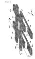
- Figure 5 is a perspective view showing an example of a quantum logic device according to an embodiment of the present invention.
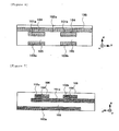
- Figure 6 is a sectional view taken along line A-A of Figure 5 .
- Figure 7 is a sectional view taken along line B-B of Figure 5 .
- a quantum logic device embodying the present invention includes a first conducting member 101a, a first conducting member 101b, a second conducting member 102a, a second conducting member 102b, a third conducting member 103a, and a third conducting member 103b.
- the quantum logic device shown in Figure 5 has two quantum logic devices and will be described in detail later.
- An insulating member 104 is formed between the first conducting members 101a and 101b and the second conducting members 102a and 102b, and an insulating member 105 is formed between the first conducting members idea and 101b and the third conducting members 103a and 103b.
- the insulating member 104 and the insulating member 105 can each be formed as one member in xy plane.
- FIG. 5 only shows a part interposed between the first conducting members 101a and 101b and the second conducting members 102a and 102b and a part interposed between the first conducting members 101a and 101b and the third conducting members 103a and 103b.
- An insulating member 106 (not shown in Figure 5 ) is formed on +z side of the second conducting members 102a and 102b, and an insulating member (not shown in Figures 5 to 7 ) is formed on -z side of the third conducting members 103a and 103b.
- an external electrode (not shown) for injecting and extracting carriers (electrons) is connected to each conducting member 102a, 101b, 102a, 102b, 103a, and 103b.
- the conducting members 101a, 101b, 102a, 102b, 103a, and 103b are members formed in straight lines and are disposed according to a spatial arrangement shown in Figure 5 . That is, the first conducting members 101a and 101b are formed in straight lines stretching in x direction and are arranged on xy plane.
- the second conducting members 102a and 102b are formed in straight lines stretching in y direction and are arranged on xy plane which is higher in z direction than the plane where the first conducting members 101a and 101b are arranged. That is, the first conducing members 101a and 101b and the second conducting members 102a and 102b intersect each other taken along z direction.
- the third conducting members 103a and 103b are formed in straight lines stretching in x direction, are arranged on xy plane which is lower in -z direction than the plane where the first conducting members 101a and 101b are arranged, and are arranged along the first conducting members 101a and 101b.
- the first conducting members 101a and 101b have a thickness of several nm in z direction
- the first conducting member 101a (first conducting member 101b), the insulating member 104, and the insulating member 105 constitute a quantum well (QW) in z direction.
- QW quantum well
- carriers electrons
- 2DEG two-dimensional electron gas
- the materials of the first conducting members 101a and 101b are not particularly limited as long as the conducting members constitute the quantum well
- the second conducting members 102a and 102b have a thickness of, e.g., several nm in z direction
- the second conducting member 102a (second conducting member 102b), the insulating member 104, and the insulating member 106 (not shown in Figure 5 ) provided in +z direction constitute a quantum well (QW) in z direction.
- QW quantum well
- the second conducting members 102a and 102b it is not necessary to quantize the second conducting members 102a and 102b in x direction and y direction, so that carriers are not confined in x direction and y direction.
- electrons in the second conducting members 102a and 102b become a two-dimensional electrons gas (2DEG) spreading over the xy plane.
- the materials of the second conducting members 102a and 102b are not particularly limited as long as the conducting members constitute the quantum well.
- the third conducting members 103a and 103b have the function of generating an electrostatic field affecting the first conducting members 101a and 101b.
- the materials of the third conducting members 103a and 103b are not particularly limited.
- the insulating member 104 is an insulating film formed between the first conducting members 101a and 101b and the second conducting members 102a and 102b.
- the insulating member 104 has a small thickness enough to pass a large tunnel current.
- the insulating member 104 is several nm or smaller in thickness.
- the material of the insulating member 104 is not particularly limited as long as the material can form the quantum well and the material can be small in thickness enough to pass tunnel current.
- the insulating member 105 is an insulating film formed between the first conducting members 101a and 101b and the third conducting members 103a and 103b.
- the insulating member 105 is larger in thickness than the insulating member 104 or is made of a material of a high tunnel barrier so as to pass a smaller tunnel current
- the insulating member 105 is several nm to several tens of nm in thickness.
- the material of the insulating member 105 is not particularly limited as long as the quantum well can be formed and the material has a preferred insulating characteristic.
- the first conducting member 101a, the second conducting member 102a, the third conducting member 103a, the insulating member 104, and the insulating member 105 constitute one quantum device
- the members are associated with the quantum device as follows: the first conducting member 101a corresponds to a first quantum structure area and a first electrode area in the quantum device, the second conducting member 102a corresponds to a second quantum structure area and a second electrode area in the quantum device, the third conducting member 103a corresponds to a carrier conduction area in the quantum device, a part of the insulating member 104 corresponds to a tunnel barrier area in the quantum device, and a part of the insulating member 105 corresponds to an isolation area in the quantum device.
- the first conducting member 101a and the second conducting member 102a intersect each other taken along z direction.
- An overlap at the intersection taken along the z direction forms a coupled quantum well of the quantum device.
- the overlap of the first conducting member 101a corresponds to the first quantum structure area of the quantum device and the portion other than the overlap of the first conducting member 101a corresponds to the first electrode area of the quantum device.
- the overlap of the second conducting member 102a corresponds to the second quantum structure area of the quantum device and the portion other than the overlap of the second conducting member 102a corresponds to the second electrode area of the quantum device.
- the portions other than the overlap of the first conducting member 101a and the second conducting member 102a are provided to inject carriers to the overlap from thexy plane orthogonal to z direction, and the portions other than the overlap do not disturb the quantum confined state of the overlap.
- Another three quantum devices are configured by combining the members in a similar manner.
- the another quantum devices are a combination of the first conducting member 101a, the second conducting member 102b, the third conducting member 103a, the insulating member 104, and the insulating member 105, a combination of the first conducting member 101b, the second conducting member 102a, the third conducting member 103b, the insulating member 104, and the insulating member 105, or a combination of the first conducting member 101b, the second conducting member 102b, the third conducting member 103b, the insulating member 104, and the insulating member 105.
- the quantum logic device of Figure 5 includes the four quantum devices. Of these quantum devices, two quantum devices along x direction constitute one quantum logic device. That is, the quantum logic device shown in Figure 5 includes two quantum logic devices.
- Figure 8 schematically shows a quantum logic device.
- the quantum logic device of Figure 8 is constituted of members shown in the sectional view of Figure 7 .
- the quantum devices included in the quantum logic device of Figure 5 are equivalents and thus it is not necessary to discriminate the members such as the first conducting member 101a by adding subscripts including "a” and "b".
- the members having the same function are indicated by common reference numerals and the discrimination using subscripts such as "a” and “b” is omitted unless otherwise specified.
- the common reference numerals are used in the schematic diagram of Figure 8.
- Figure 8 shows that negative differential resistance elements NDR are inserted between the first conducting member 101 and the second conducting member 102 and associate an I-V characteristic of the quantum device.
- an input IN, an output OUT, an input ⁇ , and an inverted input ⁇ bar are shown as inputs and outputs.
- the second conducting member fed with the ⁇ and ⁇ bar the second conducting member fed with the ⁇ bar is denoted as 102b.
- the NDR between the second conducting member 102b and the first conducting member 101 is denoted as NDRb.
- the two quantum devices are connected in parallel. That is, the first quantum structure area and a carrier conduction area of each quantum device are connected in parallel.
- the quantum logic device of Figure 8 is shown as an equivalent circuit in Figure 9.
- Figure 9 is a circuit diagram showing the equivalent circuit of the quantum logic device of Figure 8 .
- the subband of the first conducting member 101 (first quantum structure area) is controlled by an electrostatic field from a third conduction area via the insulating member 105.
- the Fermi level of the first conducting member 101 is so controlled as to match with one (or both) of the potentials of two second conduction areas (second quantum structure area) via NDR or NDRb. In this case, the potential of the output OUT matches with the Fermi level of the first conducting member 101.
- Figure 10 is a diagram for explaining the operations of the quantum logic device of Figure 8 .
- Figure 10(a) is a time chart
- Figure 10(b) is a band diagram
- Figure 10(c) is an I-V characteristic diagram.
- the vertical axis indicates the voltages of clock, input, and output signals and the horizontal axis indicates time.
- the input signal IN is inputted in synchronization with a first clock CLK in the uppermost part of Figure 10(a) .
- Reference character IN denotes a signal which is, e.g., 0.5 V in an equalized state (neutral state) and 0 V or 1 V during application (in an active state).
- the ⁇ and ⁇ bar are inputted in synchronization with a second clock CLKD in the second uppermost part of Figure 10(a) .
- the second clock CLKD is a clock signal which is delayed by a predetermined phase from the first clock CLK.
- the predetermined phase is about 2 ⁇ /8 to 2 ⁇ /3 and is not particularly limited as long as a normal operation is obtained.
- voltage is applied to IN generated from a circuit operating in synchronization with the first clock CLK, thereby obtaining a reliable operation.
- CLK and CLKD were described for comparison and association with a normal synchronous circuit. CLK and CLKD are not always necessary in the system of the present application.
- ⁇ denotes a signal which has 0.5 V in the equalized state (neutral state) and 1 V during application.
- the ⁇ bar denotes a signal which has 0.5 V in the equalized state and 0 V during application.
- the voltages 0 V, 0.5 V, and 1 V are just examples and thus a voltage amplitude may be reduced or increased.
- the voltage of 0.5 V in the equalized state is also an example. Any voltage is applicable in the equalized state as long as the voltage is an intermediate voltage of a signal amplitude.
- the band diagram of Figure 10(b) shows the potentials of the first conducting member 101, the second conducting member 102, and the second conducting member 102b when the signals are applied in the time chart.
- Figure 10(b) shows five band diagrams corresponding times t1 to t5 in the timing chart of Figure 10(a) .
- QW on the left corresponds to the second conducting member 102 connected to ⁇
- QW at the center corresponds to the first conducting member 101 connected to OUT
- QW on the right corresponds to the second conducting member 102b connected to the ⁇ bar.
- 2DEG is displayed on QW in each of the band diagrams.
- the lower end of 2DEG corresponds to a subband level and the upper end of 2DEG corresponds to the Fermi level.
- Figure 10(c) is a graph showing the I-V characteristics of the times t1 to t5 (i.e., the potential states of Figure 10(b) ).
- Each of the I-V characteristic graphs in Figure 10(c) shows two I-V curves.
- a solid line curve indicates an I-V characteristic between the second conducting member 102b and the first conducting member 101 (i.e., between the ⁇ bar and OUT) and a broken line curve indicates an I-V characteristic between the second conducting member 102 and the first conducting member 101 (i.e., between ⁇ and OUT).
- the intersection point of the dotted line curve and the broken line curve is an operating point of the first conducting member 101.
- the two NDRs (NDR and NDRb) are both turned on and there is continuity between the ⁇ and ⁇ bar (the I-V characteristic diagram corresponding to t1).
- the ⁇ and ⁇ bar are both equalized at 0.5 V, no current is fed and OUT has a voltage of 0.5 V.
- the I-V curve (solid line) between the first conducting member 101 and the second conducting member 102b increases in peak (moves in a direction of passing a larger current)
- the I-V curve (broken line) between the first conducting member 101 and the second conducting member 102 decreases in peak (moves in a direction of feeding a smaller current).
- the quantum logic device having the input/output configuration of Figure 8 acts as a latch circuit.
- Figure 12 shows a device schematic diagram and a truth table indicating that a quantum logic device similar to that of Figure 8 has a different input/output configuration.
- ORIN is inputted instead of IN of Figure 8
- IN1 is inputted instead of ⁇
- IN2 is inputted instead of the ⁇ bar.
- ORIN is a signal of "1 V" which is applied earlier than ⁇ , e.g., in synchronization with a clock CLK.
- "1 V" is variable as described above.
- the device of Figure 12 obtains an OR logic. The operations of the quantum logic device having the input/output configuration are evident from the above description.
- Figure 13 shows a device schematic diagram and a truth table indicating that a quantum logic device similar to that of Figure 8 has still another input/output configuration.
- ANDIN is inputted instead of IN of Figure 8
- IN1 is inputted instead of ⁇
- IN2 is inputted instead of the ⁇ bar.
- ANDIN is a signal of "0 V” which is applied earlier than ⁇ , e.g., in synchronization with the clock CLK. "0 V” is variable as described above.
- the device of Figure 13 obtains an AND logic. The operations of the quantum logic device having the input/output configuration are also evident from the above description.
- the logic circuits of latch, AND, and OR can be configured by changing the input/output configuration in the quantum logic device of the present embodiment.
- the quantum logic device shown in Figure 5 includes two quantum logic devices which can constitute the logic circuits of latch, AND, and OR.
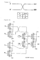
- a NOT logic can be readily implemented by causing the two quantum logic devices to perform differential operations in a complementary manner. That is, as shown in Figure 14 , the NOT logic can be readily implemented by causing the input IN and an inverse signal IN bar intersect each other to produce an output OUT and an OUT bar.
- the logic circuits AND and OR of the quantum logic device and the NOT logic of the complementary circuit configuration are implemented, achieving a basic logic circuit which can constitute a given logic circuit.
- a given logic can be configured using a combinational logic circuit of the basic logic circuits.
- a given sequential circuit can be implemented using the latch circuit composed of the quantum logic devices. That is, it is possible to achieve a system consistent with the implementation of a classical computers using existing sequential circuits.
- Figure 15 shows an example of a logic circuit when the quantum logic device of the present embodiment is applied to a circuit configuration in a differential mode.
- a charge supplied as an input is used as an output in logic circuits of AND, OR, and NOT.
- an inputted charge can be reused (charge recycling) in the logic circuit of the subsequent stage, thereby reducing power consumption.
- Charge recycling can be used over two or more stages as long as a sufficient energy can be obtained as an input.
- a latch circuit may be used.
- a known method of forming a thin film, lithography, and etching are applicable for manufacturing the quantum logic device of the present embodiment.
- the quantum logic device can be manufactured by properly combining the known thin-film forming and processing methods.
- manufacturing processes requiring the finest forming and processing techniques are a process of forming a thin film serving as the first conducting member, a process of forming a thin film serving as the insulating member 104, and a process of forming a thin film serving as the second conducting member.
- film formation and micromachining of several nm have difficulties particularly in the process of lithography and etching.
- a thin film on the order of several nm can be formed with relative ease by using molecular beam epitaxy and MO-CVD, so that the quantum logic device can be manufactured using these methods of forming thin films.
- the quantum well (QW) for generating 2DGE as a quantum structure area to be quantized.
- a quantum structure area of the present invention has quantization in one direction (z direction in the present embodiment) and quantization may be performed in x direction or both in x direction and y direction.
- the present invention relates to a quantum logic device and a logic circuit which can be implemented in a system consistent with the implementation of a classical computer.
- the present invention can be used in an information processing industry such as computer industry.
Landscapes
- Logic Circuits (AREA)
- Junction Field-Effect Transistors (AREA)
- Thin Film Transistor (AREA)
- Bipolar Transistors (AREA)
Claims (9)
- Unité logique quantique comprenant :un premier élément conducteur (101a) qui s'étend dans une première direction et disposé sur un premier plan ;une paire de seconds éléments conducteurs (102a, 102b) qui s'étendent dans une seconde direction différente de la première direction et disposés sur un deuxième plan parallèle au premier plan, chacun des seconds éléments conducteurs (102a, 102b) chevauchant le premier élément conducteur au niveau d'une intersection, la région du premier élément conducteur au niveau d'une telle intersection formant une première zone de structure quantique, la région de chaque second élément conducteur au niveau d'une telle intersection formant une seconde zone de la structure quantique, les première et seconde zones quantiques étant chacune destinée à confiner un porteur de charge au moins dans une direction perpendiculaire aux premier et second plans, la région du premier élément conducteur éloignée de l'intersection formant une première zone d'électrode pour injecter un porteur de charge dans la première zone de structure quantique à partir d'une direction parallèle au premier plan, la région de chaque second élément conducteur éloignée de l'intersection formant une seconde zone d'électrode pour injecter un porteur de charge dans la seconde zone de structure quantique correspondante à partir d'une direction parallèle au second plan ;un premier élément isolant (104) disposé entre les premier et second éléments conducteurs, la région de l'élément isolant au niveau de l'intersection formant une zone barrière à effet tunnel entre les première et seconde zones de structure quantique ;un troisième élément conducteur (103) qui s'étend dans la première direction et disposé sur un troisième plan parallèle au premier plan, la région du troisième élément conducteur au niveau de l'intersection formant une zone de conduction de porteur ;un second élément isolant (105) disposé entre les premier et troisième éléments conducteurs, la seconde zone isolante formant une zone d'isolement entre la première zone de structure quantique et la zone de conduction de porteur ;l'unité logique quantique pouvant être configuré, selon le cas, en : un circuit de verrouillage dans lequel la zone de conduction de porteur sert d'entrée, la première zone d'électrode sert de sortie, l'une des secondes zones d'électrode est mise à un état logique « 1 », et l'autre des secondes zones d'électrode est mise à un état logique « 0 » ; un circuit logique OU dans lequel la paire de secondes zones d'électrode sert d'entrées, la première zone d'électrode sert de sortie, et la zone de conduction de porteur est mise à un état logique « 1 » ; et, un circuit logique ET dans lequel la paire de secondes zones d'électrode sert d'entrées, la première zone d'électrode sert de sortie, et la zone de conduction de porteur est mise à un état logique « 0 ».
- Unité logique quantique comportant une unité quantique selon la revendication 1, comprenant des première et seconde zones de conduction de porteur.
- Système de commande de circuit logique pour une unité logique quantique selon la revendication 1 ou 2, dans lequel un signal est appliqué à la zone de conduction de porteur en synchronisme avec un premier signal d'horloge, et des signaux sont appliqués aux secondes zones d'électrode en synchronisme avec un second signal d'horloge retardé par rapport au signal d'horloge d'une phase prédéterminée.
- Système de commande de circuit logique de l'unité logique quantique selon la revendication 3, comprenant une période d'égalisation pour égaliser des potentiels de la première zone de structure quantique, la seconde zone de structure quantique, et la zone de conduction de porteur à partir du moment où des signaux sont appliqués aux secondes zones d'électrode jusqu'au moment où un signal est appliqué à la zone de conduction de porteur.
- Circuit logique de combinaison comprenant une ou plusieurs unités logiques quantiques selon la revendication 1.
- Unité logique quantique selon la revendication 1, dans lequel une tension appliquée à la zone de conduction de porteur modifie les caractéristiques I-IV entre la première zone d'électrode et la seconde zone d'électrode.
- Unité logique quantique selon la revendication 1, dans lequel les première et seconde zones de structure quantique sont, selon le cas, un puits quantique, un fil quantique, et un point quantique.
- Unité logique quantique selon la revendication 1, dans lequel un niveau de sous-bande des premières zones de structure quantique est commandé par un champ électrique généré par la zone de conduction de porteur, le niveau de sous-bande étant généré en confinant un porteur dans les premières zones de structure quantique ; et,
un niveau de Fermi du porteur des premières zones de structure quantique est commandé par un potentiel appliqué à la première zone d'électrode et des potentiels appliqués aux secondes zones d'électrode lorsque les premières zones de structure quantique et les secondes zones de structure quantique sont couplées en résonance. - Unité quantique selon la revendication 1, comprenant en outre :un état de résistance différentielle positive qui apparaît en raison d'un effet tunnel d'un couplage résonnant entre les premières zones de structure quantique et les secondes zones de structure quantique, le couplage résonnant se produisant entre des fonctions d'état des niveaux d'énergie des premières zones de structure quantique et des secondes zones de structure quantique en raison d'une différence de potentiel entre les premières zones de structure quantique et des secondes zones de structure quantique ;un état de résistance différentielle négative qui apparaît entre les premières zones de structure quantique et les secondes zones de structure quantique en raison d'un chevauchement des fonctions d'état des niveaux d'énergie se propageant vers la zone barrière à effet tunnel, et d'un couplage résonnant réduit ; etun état d'isolement entre les premières zones de structure quantique et les secondes zones de structure quantique, l'état d'isolement ayant un couplage résonnant ou un chevauchement des fonctions d'état négligeable.
Applications Claiming Priority (2)
| Application Number | Priority Date | Filing Date | Title |
|---|---|---|---|
| JP2004162425 | 2004-05-31 | ||
| PCT/JP2005/009693 WO2005117127A1 (fr) | 2004-05-31 | 2005-05-26 | Dispositif quantique, dispositif de logique quantique, méthode de commande de dispositif de logique quantique et de circuit logique par dispositif de logique quantique |
Publications (3)
| Publication Number | Publication Date |
|---|---|
| EP1753031A1 EP1753031A1 (fr) | 2007-02-14 |
| EP1753031A4 EP1753031A4 (fr) | 2011-06-01 |
| EP1753031B1 true EP1753031B1 (fr) | 2014-02-26 |
Family
ID=35451158
Family Applications (1)
| Application Number | Title | Priority Date | Filing Date |
|---|---|---|---|
| EP05743368.2A Expired - Lifetime EP1753031B1 (fr) | 2004-05-31 | 2005-05-26 | Dispositif de logique quantique et circuit logique par dispositif de logique quantique |
Country Status (7)
| Country | Link |
|---|---|
| US (1) | US7956348B2 (fr) |
| EP (1) | EP1753031B1 (fr) |
| JP (1) | JP4965248B2 (fr) |
| KR (1) | KR100843492B1 (fr) |
| CN (1) | CN1950944B (fr) |
| TW (1) | TWI330889B (fr) |
| WO (1) | WO2005117127A1 (fr) |
Families Citing this family (12)
| Publication number | Priority date | Publication date | Assignee | Title |
|---|---|---|---|---|
| AU2005307201A1 (en) * | 2004-11-22 | 2006-05-26 | Kent, Stephen Christopher | Electric field sensing device |
| JP2008306618A (ja) * | 2007-06-11 | 2008-12-18 | Nissan Motor Co Ltd | 電圧駆動型素子を駆動するための駆動回路 |
| US7667499B2 (en) * | 2007-06-11 | 2010-02-23 | Infineon Technologies Ag | MuGFET circuit for increasing output resistance |
| JP5573850B2 (ja) * | 2010-01-15 | 2014-08-20 | 独立行政法人国立高等専門学校機構 | 論理回路および集積回路 |
| TWI469325B (zh) * | 2012-07-31 | 2015-01-11 | 財團法人工業技術研究院 | 邏輯閘 |
| JP6150478B2 (ja) * | 2012-08-29 | 2017-06-21 | 公益財団法人電磁材料研究所 | 複相構造薄膜材料 |
| JP2018098338A (ja) | 2016-12-13 | 2018-06-21 | ソニーセミコンダクタソリューションズ株式会社 | トンネル電界効果トランジスタ |
| US11074382B2 (en) | 2018-01-30 | 2021-07-27 | International Business Machines Corporation | Quantum computing device design |
| JP7244388B2 (ja) * | 2019-08-05 | 2023-03-22 | 株式会社日立製作所 | 量子情報処理装置及び量子ビットアレイ |
| DE112021007421B4 (de) * | 2021-05-28 | 2025-01-23 | Mitsubishi Electric Corporation | Ladungssensor |
| CN117249914B (zh) * | 2022-06-09 | 2025-08-19 | 思特威(上海)电子科技股份有限公司 | 温度传感器的增益调节电路及温度传感器 |
| CN115374947B (zh) * | 2022-10-25 | 2022-12-20 | 上海芯联芯智能科技有限公司 | 量子点胞自动机电路与其运作方法 |
Family Cites Families (13)
| Publication number | Priority date | Publication date | Assignee | Title |
|---|---|---|---|---|
| JPH0783111B2 (ja) | 1986-10-07 | 1995-09-06 | ソニー株式会社 | 超高速半導体装置 |
| US5312684A (en) * | 1991-05-02 | 1994-05-17 | Dow Corning Corporation | Threshold switching device |
| US5347140A (en) * | 1991-08-27 | 1994-09-13 | Matsushita Electric Industrial Co., Ltd. | Resonant electron transfer device |
| JP3361135B2 (ja) | 1991-12-20 | 2003-01-07 | テキサス インスツルメンツ インコーポレイテツド | 量子効果論理ユニットとその製造方法 |
| US5414274A (en) | 1993-07-26 | 1995-05-09 | Motorola, Inc. | Quantum multifunction transistor with gated tunneling region |
| US6333516B1 (en) * | 1993-09-16 | 2001-12-25 | Kabushiki Kaisha Toshiba | Quantum effect device |
| JPH09312378A (ja) * | 1996-03-19 | 1997-12-02 | Fujitsu Ltd | 半導体装置及びその製造方法 |
| US5903170A (en) | 1997-06-03 | 1999-05-11 | The Regents Of The University Of Michigan | Digital logic design using negative differential resistance diodes and field-effect transistors |
| US6987282B2 (en) * | 2000-12-22 | 2006-01-17 | D-Wave Systems, Inc. | Quantum bit with a multi-terminal junction and loop with a phase shift |
| EP1262911A1 (fr) * | 2001-05-30 | 2002-12-04 | Hitachi Europe Limited | Ordinateur quantique |
| US6978070B1 (en) * | 2001-08-14 | 2005-12-20 | The Programmable Matter Corporation | Fiber incorporating quantum dots as programmable dopants |
| US7462857B2 (en) * | 2002-09-19 | 2008-12-09 | Sharp Kabushiki Kaisha | Memory device including resistance-changing function body |
| KR100662875B1 (ko) * | 2004-04-16 | 2007-01-02 | 한국광기술원 | 반가산기를 이용한 논리연산장치 |
-
2005
- 2005-05-02 TW TW094114080A patent/TWI330889B/zh not_active IP Right Cessation
- 2005-05-26 US US11/569,855 patent/US7956348B2/en active Active
- 2005-05-26 EP EP05743368.2A patent/EP1753031B1/fr not_active Expired - Lifetime
- 2005-05-26 WO PCT/JP2005/009693 patent/WO2005117127A1/fr not_active Ceased
- 2005-05-26 KR KR1020067021407A patent/KR100843492B1/ko not_active Expired - Lifetime
- 2005-05-26 CN CN2005800145508A patent/CN1950944B/zh not_active Expired - Lifetime
- 2005-05-26 JP JP2006513953A patent/JP4965248B2/ja not_active Expired - Lifetime
Also Published As
| Publication number | Publication date |
|---|---|
| TW200610145A (en) | 2006-03-16 |
| US7956348B2 (en) | 2011-06-07 |
| EP1753031A4 (fr) | 2011-06-01 |
| WO2005117127A1 (fr) | 2005-12-08 |
| TWI330889B (en) | 2010-09-21 |
| KR20070004846A (ko) | 2007-01-09 |
| JPWO2005117127A1 (ja) | 2008-07-31 |
| US20090051384A1 (en) | 2009-02-26 |
| KR100843492B1 (ko) | 2008-07-04 |
| CN1950944B (zh) | 2010-08-25 |
| EP1753031A1 (fr) | 2007-02-14 |
| CN1950944A (zh) | 2007-04-18 |
| JP4965248B2 (ja) | 2012-07-04 |
Similar Documents
| Publication | Publication Date | Title |
|---|---|---|
| EP1753031B1 (fr) | Dispositif de logique quantique et circuit logique par dispositif de logique quantique | |
| US5447873A (en) | Method of making a universal quantum dot logic cell | |
| JP3922466B2 (ja) | 半導体論理素子 | |
| Takahashi et al. | Silicon single-electron devices and their applications | |
| Ahmed et al. | Single-electron devices | |
| Wang | Issues of nanoelectronics: A possible roadmap | |
| EP1028472B1 (fr) | Dispsoitif à blocage de Coulomb et procédé pour sa fabrication | |
| Jain et al. | Quantum dot channel (QDC) FETs with wraparound II–VI gate insulators: Numerical simulations | |
| Gholipour et al. | Design investigation of nanoelectronic circuits using crossbar-based nanoarchitectures | |
| US7208753B2 (en) | Enhancement mode single electron transistor | |
| Bate | Nanoelectronics | |
| Schmid et al. | Robust circuit and system design methodologies for nanometer-scale devices and single-electron transistors | |
| Uemura et al. | A three-valued D-flip-flop and shift register using multiple-junction surface tunnel transistors | |
| Nakazato | Single-electron switch for phase-locked single-electron logic devices | |
| Eachempati et al. | Reconfigurable BDD based quantum circuits | |
| Jain et al. | Four-State Sub-12-nm FETs Employing Lattice-Matched II–VI Barrier Layers | |
| Liu et al. | A reconfigurable low-power BDD logic architecture using ferroelectric single-electron transistors | |
| JPH07161965A (ja) | 半導体装置及び多値論理回路 | |
| Goser et al. | System and circuit aspects of nanoelectronics | |
| Haron et al. | Emerging non-CMOS nanoelectronic devices-What are they? | |
| Baba et al. | Development of InGaAs-based multiple-junction surface tunnel transistors for multiple-valued logic circuits | |
| Wolpert et al. | Ballistic deflection transistors and the emerging nanoscale era | |
| Dongale et al. | Shifting towards Nanoelectronics: A device level overview | |
| Amakawa et al. | multiple-tunnel junctions | |
| EP0802633B1 (fr) | Circuit logique selon un diagramme de décision binaire |
Legal Events
| Date | Code | Title | Description |
|---|---|---|---|
| PUAI | Public reference made under article 153(3) epc to a published international application that has entered the european phase |
Free format text: ORIGINAL CODE: 0009012 |
|
| 17P | Request for examination filed |
Effective date: 20061127 |
|
| AK | Designated contracting states |
Kind code of ref document: A1 Designated state(s): AT BE BG CH CY CZ DE DK EE ES FI FR GB GR HU IE IS IT LI LT LU MC NL PL PT RO SE SI SK TR |
|
| DAX | Request for extension of the european patent (deleted) | ||
| A4 | Supplementary search report drawn up and despatched |
Effective date: 20110502 |
|
| 17Q | First examination report despatched |
Effective date: 20110715 |
|
| GRAP | Despatch of communication of intention to grant a patent |
Free format text: ORIGINAL CODE: EPIDOSNIGR1 |
|
| GRAJ | Information related to disapproval of communication of intention to grant by the applicant or resumption of examination proceedings by the epo deleted |
Free format text: ORIGINAL CODE: EPIDOSDIGR1 |
|
| GRAP | Despatch of communication of intention to grant a patent |
Free format text: ORIGINAL CODE: EPIDOSNIGR1 |
|
| INTG | Intention to grant announced |
Effective date: 20131003 |
|
| INTG | Intention to grant announced |
Effective date: 20131021 |
|
| GRAS | Grant fee paid |
Free format text: ORIGINAL CODE: EPIDOSNIGR3 |
|
| GRAA | (expected) grant |
Free format text: ORIGINAL CODE: 0009210 |
|
| AK | Designated contracting states |
Kind code of ref document: B1 Designated state(s): AT BE BG CH CY CZ DE DK EE ES FI FR GB GR HU IE IS IT LI LT LU MC NL PL PT RO SE SI SK TR |
|
| REG | Reference to a national code |
Ref country code: GB Ref legal event code: FG4D |
|
| REG | Reference to a national code |
Ref country code: CH Ref legal event code: NV Representative=s name: IBM RESEARCH GMBH ZURICH RESEARCH LABORATORY I, CH Ref country code: CH Ref legal event code: EP |
|
| REG | Reference to a national code |
Ref country code: AT Ref legal event code: REF Ref document number: 654033 Country of ref document: AT Kind code of ref document: T Effective date: 20140315 |
|
| REG | Reference to a national code |
Ref country code: GB Ref legal event code: 746 Effective date: 20140305 |
|
| REG | Reference to a national code |
Ref country code: IE Ref legal event code: FG4D |
|
| REG | Reference to a national code |
Ref country code: DE Ref legal event code: R096 Ref document number: 602005042761 Country of ref document: DE Effective date: 20140410 |
|
| REG | Reference to a national code |
Ref country code: DE Ref legal event code: R084 Ref document number: 602005042761 Country of ref document: DE Effective date: 20140304 |
|
| REG | Reference to a national code |
Ref country code: NL Ref legal event code: VDEP Effective date: 20140226 |
|
| REG | Reference to a national code |
Ref country code: AT Ref legal event code: MK05 Ref document number: 654033 Country of ref document: AT Kind code of ref document: T Effective date: 20140226 |
|
| REG | Reference to a national code |
Ref country code: LT Ref legal event code: MG4D |
|
| PG25 | Lapsed in a contracting state [announced via postgrant information from national office to epo] |
Ref country code: IS Free format text: LAPSE BECAUSE OF FAILURE TO SUBMIT A TRANSLATION OF THE DESCRIPTION OR TO PAY THE FEE WITHIN THE PRESCRIBED TIME-LIMIT Effective date: 20140626 Ref country code: LT Free format text: LAPSE BECAUSE OF FAILURE TO SUBMIT A TRANSLATION OF THE DESCRIPTION OR TO PAY THE FEE WITHIN THE PRESCRIBED TIME-LIMIT Effective date: 20140226 |
|
| PG25 | Lapsed in a contracting state [announced via postgrant information from national office to epo] |
Ref country code: AT Free format text: LAPSE BECAUSE OF FAILURE TO SUBMIT A TRANSLATION OF THE DESCRIPTION OR TO PAY THE FEE WITHIN THE PRESCRIBED TIME-LIMIT Effective date: 20140226 Ref country code: CY Free format text: LAPSE BECAUSE OF FAILURE TO SUBMIT A TRANSLATION OF THE DESCRIPTION OR TO PAY THE FEE WITHIN THE PRESCRIBED TIME-LIMIT Effective date: 20140226 Ref country code: SE Free format text: LAPSE BECAUSE OF FAILURE TO SUBMIT A TRANSLATION OF THE DESCRIPTION OR TO PAY THE FEE WITHIN THE PRESCRIBED TIME-LIMIT Effective date: 20140226 Ref country code: FI Free format text: LAPSE BECAUSE OF FAILURE TO SUBMIT A TRANSLATION OF THE DESCRIPTION OR TO PAY THE FEE WITHIN THE PRESCRIBED TIME-LIMIT Effective date: 20140226 Ref country code: PT Free format text: LAPSE BECAUSE OF FAILURE TO SUBMIT A TRANSLATION OF THE DESCRIPTION OR TO PAY THE FEE WITHIN THE PRESCRIBED TIME-LIMIT Effective date: 20140626 Ref country code: NL Free format text: LAPSE BECAUSE OF FAILURE TO SUBMIT A TRANSLATION OF THE DESCRIPTION OR TO PAY THE FEE WITHIN THE PRESCRIBED TIME-LIMIT Effective date: 20140226 |
|
| PG25 | Lapsed in a contracting state [announced via postgrant information from national office to epo] |
Ref country code: BE Free format text: LAPSE BECAUSE OF FAILURE TO SUBMIT A TRANSLATION OF THE DESCRIPTION OR TO PAY THE FEE WITHIN THE PRESCRIBED TIME-LIMIT Effective date: 20140226 |
|
| PG25 | Lapsed in a contracting state [announced via postgrant information from national office to epo] |
Ref country code: RO Free format text: LAPSE BECAUSE OF FAILURE TO SUBMIT A TRANSLATION OF THE DESCRIPTION OR TO PAY THE FEE WITHIN THE PRESCRIBED TIME-LIMIT Effective date: 20140226 Ref country code: EE Free format text: LAPSE BECAUSE OF FAILURE TO SUBMIT A TRANSLATION OF THE DESCRIPTION OR TO PAY THE FEE WITHIN THE PRESCRIBED TIME-LIMIT Effective date: 20140226 Ref country code: DK Free format text: LAPSE BECAUSE OF FAILURE TO SUBMIT A TRANSLATION OF THE DESCRIPTION OR TO PAY THE FEE WITHIN THE PRESCRIBED TIME-LIMIT Effective date: 20140226 Ref country code: CZ Free format text: LAPSE BECAUSE OF FAILURE TO SUBMIT A TRANSLATION OF THE DESCRIPTION OR TO PAY THE FEE WITHIN THE PRESCRIBED TIME-LIMIT Effective date: 20140226 |
|
| REG | Reference to a national code |
Ref country code: DE Ref legal event code: R097 Ref document number: 602005042761 Country of ref document: DE |
|
| PG25 | Lapsed in a contracting state [announced via postgrant information from national office to epo] |
Ref country code: ES Free format text: LAPSE BECAUSE OF FAILURE TO SUBMIT A TRANSLATION OF THE DESCRIPTION OR TO PAY THE FEE WITHIN THE PRESCRIBED TIME-LIMIT Effective date: 20140226 Ref country code: PL Free format text: LAPSE BECAUSE OF FAILURE TO SUBMIT A TRANSLATION OF THE DESCRIPTION OR TO PAY THE FEE WITHIN THE PRESCRIBED TIME-LIMIT Effective date: 20140226 Ref country code: SK Free format text: LAPSE BECAUSE OF FAILURE TO SUBMIT A TRANSLATION OF THE DESCRIPTION OR TO PAY THE FEE WITHIN THE PRESCRIBED TIME-LIMIT Effective date: 20140226 |
|
| PG25 | Lapsed in a contracting state [announced via postgrant information from national office to epo] |
Ref country code: LU Free format text: LAPSE BECAUSE OF FAILURE TO SUBMIT A TRANSLATION OF THE DESCRIPTION OR TO PAY THE FEE WITHIN THE PRESCRIBED TIME-LIMIT Effective date: 20140526 |
|
| REG | Reference to a national code |
Ref country code: CH Ref legal event code: PL |
|
| PLBE | No opposition filed within time limit |
Free format text: ORIGINAL CODE: 0009261 |
|
| STAA | Information on the status of an ep patent application or granted ep patent |
Free format text: STATUS: NO OPPOSITION FILED WITHIN TIME LIMIT |
|
| PG25 | Lapsed in a contracting state [announced via postgrant information from national office to epo] |
Ref country code: LI Free format text: LAPSE BECAUSE OF NON-PAYMENT OF DUE FEES Effective date: 20140531 Ref country code: MC Free format text: LAPSE BECAUSE OF FAILURE TO SUBMIT A TRANSLATION OF THE DESCRIPTION OR TO PAY THE FEE WITHIN THE PRESCRIBED TIME-LIMIT Effective date: 20140226 Ref country code: CH Free format text: LAPSE BECAUSE OF NON-PAYMENT OF DUE FEES Effective date: 20140531 |
|
| 26N | No opposition filed |
Effective date: 20141127 |
|
| REG | Reference to a national code |
Ref country code: IE Ref legal event code: MM4A |
|
| REG | Reference to a national code |
Ref country code: FR Ref legal event code: ST Effective date: 20150130 |
|
| REG | Reference to a national code |
Ref country code: DE Ref legal event code: R097 Ref document number: 602005042761 Country of ref document: DE Effective date: 20141127 |
|
| PG25 | Lapsed in a contracting state [announced via postgrant information from national office to epo] |
Ref country code: IT Free format text: LAPSE BECAUSE OF FAILURE TO SUBMIT A TRANSLATION OF THE DESCRIPTION OR TO PAY THE FEE WITHIN THE PRESCRIBED TIME-LIMIT Effective date: 20140226 |
|
| PG25 | Lapsed in a contracting state [announced via postgrant information from national office to epo] |
Ref country code: IE Free format text: LAPSE BECAUSE OF NON-PAYMENT OF DUE FEES Effective date: 20140526 |
|
| PG25 | Lapsed in a contracting state [announced via postgrant information from national office to epo] |
Ref country code: FR Free format text: LAPSE BECAUSE OF NON-PAYMENT OF DUE FEES Effective date: 20140602 Ref country code: SI Free format text: LAPSE BECAUSE OF FAILURE TO SUBMIT A TRANSLATION OF THE DESCRIPTION OR TO PAY THE FEE WITHIN THE PRESCRIBED TIME-LIMIT Effective date: 20140226 |
|
| PG25 | Lapsed in a contracting state [announced via postgrant information from national office to epo] |
Ref country code: BG Free format text: LAPSE BECAUSE OF FAILURE TO SUBMIT A TRANSLATION OF THE DESCRIPTION OR TO PAY THE FEE WITHIN THE PRESCRIBED TIME-LIMIT Effective date: 20140226 |
|
| PG25 | Lapsed in a contracting state [announced via postgrant information from national office to epo] |
Ref country code: GR Free format text: LAPSE BECAUSE OF FAILURE TO SUBMIT A TRANSLATION OF THE DESCRIPTION OR TO PAY THE FEE WITHIN THE PRESCRIBED TIME-LIMIT Effective date: 20140527 |
|
| PG25 | Lapsed in a contracting state [announced via postgrant information from national office to epo] |
Ref country code: TR Free format text: LAPSE BECAUSE OF FAILURE TO SUBMIT A TRANSLATION OF THE DESCRIPTION OR TO PAY THE FEE WITHIN THE PRESCRIBED TIME-LIMIT Effective date: 20140226 Ref country code: HU Free format text: LAPSE BECAUSE OF FAILURE TO SUBMIT A TRANSLATION OF THE DESCRIPTION OR TO PAY THE FEE WITHIN THE PRESCRIBED TIME-LIMIT; INVALID AB INITIO Effective date: 20050526 |
|
| REG | Reference to a national code |
Ref country code: DE Ref legal event code: R082 Ref document number: 602005042761 Country of ref document: DE Representative=s name: KUISMA, SIRPA, FI |
|
| P01 | Opt-out of the competence of the unified patent court (upc) registered |
Effective date: 20230423 |
|
| PGFP | Annual fee paid to national office [announced via postgrant information from national office to epo] |
Ref country code: GB Payment date: 20240529 Year of fee payment: 20 |
|
| PGFP | Annual fee paid to national office [announced via postgrant information from national office to epo] |
Ref country code: DE Payment date: 20240523 Year of fee payment: 20 |
|
| REG | Reference to a national code |
Ref country code: DE Ref legal event code: R079 Ref document number: 602005042761 Country of ref document: DE Free format text: PREVIOUS MAIN CLASS: H01L0029060000 Ipc: H10D0062100000 |
|
| REG | Reference to a national code |
Ref country code: DE Ref legal event code: R071 Ref document number: 602005042761 Country of ref document: DE |
|
| REG | Reference to a national code |
Ref country code: GB Ref legal event code: PE20 Expiry date: 20250525 |
|
| PG25 | Lapsed in a contracting state [announced via postgrant information from national office to epo] |
Ref country code: GB Free format text: LAPSE BECAUSE OF EXPIRATION OF PROTECTION Effective date: 20250525 |