EP1753032A1 - Halbleitersubstrat für eine solarzelle, herstellungsverfahren dafür und solarzelle - Google Patents
Halbleitersubstrat für eine solarzelle, herstellungsverfahren dafür und solarzelle Download PDFInfo
- Publication number
- EP1753032A1 EP1753032A1 EP05743744A EP05743744A EP1753032A1 EP 1753032 A1 EP1753032 A1 EP 1753032A1 EP 05743744 A EP05743744 A EP 05743744A EP 05743744 A EP05743744 A EP 05743744A EP 1753032 A1 EP1753032 A1 EP 1753032A1
- Authority
- EP
- European Patent Office
- Prior art keywords
- solar cell
- semiconductor substrate
- polycrystalline silicon
- irregularities
- solution
- Prior art date
- Legal status (The legal status is an assumption and is not a legal conclusion. Google has not performed a legal analysis and makes no representation as to the accuracy of the status listed.)
- Withdrawn
Links
- 239000000758 substrate Substances 0.000 title claims abstract description 182
- 239000004065 semiconductor Substances 0.000 title claims abstract description 68
- 238000000034 method Methods 0.000 title claims description 81
- 238000004519 manufacturing process Methods 0.000 title claims description 16
- 229910021420 polycrystalline silicon Inorganic materials 0.000 claims description 79
- 239000000243 solution Substances 0.000 claims description 43
- -1 silver ions Chemical class 0.000 claims description 30
- 229910052709 silver Inorganic materials 0.000 claims description 29
- 239000004332 silver Substances 0.000 claims description 29
- HEMHJVSKTPXQMS-UHFFFAOYSA-M Sodium hydroxide Chemical compound [OH-].[Na+] HEMHJVSKTPXQMS-UHFFFAOYSA-M 0.000 claims description 24
- 239000012670 alkaline solution Substances 0.000 claims description 15
- 239000007864 aqueous solution Substances 0.000 claims description 14
- 239000002253 acid Substances 0.000 claims description 9
- 229910002651 NO3 Inorganic materials 0.000 claims description 8
- 238000005406 washing Methods 0.000 claims description 8
- JPVYNHNXODAKFH-UHFFFAOYSA-N Cu2+ Chemical compound [Cu+2] JPVYNHNXODAKFH-UHFFFAOYSA-N 0.000 claims description 7
- 229910001431 copper ion Inorganic materials 0.000 claims description 7
- KWYUFKZDYYNOTN-UHFFFAOYSA-M Potassium hydroxide Chemical compound [OH-].[K+] KWYUFKZDYYNOTN-UHFFFAOYSA-M 0.000 claims description 6
- OAKJQQAXSVQMHS-UHFFFAOYSA-N Hydrazine Chemical compound NN OAKJQQAXSVQMHS-UHFFFAOYSA-N 0.000 claims description 4
- CDBYLPFSWZWCQE-UHFFFAOYSA-L Sodium Carbonate Chemical compound [Na+].[Na+].[O-]C([O-])=O CDBYLPFSWZWCQE-UHFFFAOYSA-L 0.000 claims description 4
- BWHMMNNQKKPAPP-UHFFFAOYSA-L potassium carbonate Chemical compound [K+].[K+].[O-]C([O-])=O BWHMMNNQKKPAPP-UHFFFAOYSA-L 0.000 claims description 4
- VHUUQVKOLVNVRT-UHFFFAOYSA-N Ammonium hydroxide Chemical compound [NH4+].[OH-] VHUUQVKOLVNVRT-UHFFFAOYSA-N 0.000 claims description 2
- 239000000908 ammonium hydroxide Substances 0.000 claims description 2
- 229910000027 potassium carbonate Inorganic materials 0.000 claims description 2
- 229910000029 sodium carbonate Inorganic materials 0.000 claims description 2
- XUIMIQQOPSSXEZ-UHFFFAOYSA-N Silicon Chemical compound [Si] XUIMIQQOPSSXEZ-UHFFFAOYSA-N 0.000 description 62
- 229910052710 silicon Inorganic materials 0.000 description 57
- 239000010703 silicon Substances 0.000 description 57
- 238000006243 chemical reaction Methods 0.000 description 52
- KRHYYFGTRYWZRS-UHFFFAOYSA-N Fluorane Chemical compound F KRHYYFGTRYWZRS-UHFFFAOYSA-N 0.000 description 33
- 239000010410 layer Substances 0.000 description 32
- 239000003929 acidic solution Substances 0.000 description 28
- GRYLNZFGIOXLOG-UHFFFAOYSA-N Nitric acid Chemical compound O[N+]([O-])=O GRYLNZFGIOXLOG-UHFFFAOYSA-N 0.000 description 19
- 229910017604 nitric acid Inorganic materials 0.000 description 19
- BQCADISMDOOEFD-UHFFFAOYSA-N Silver Chemical compound [Ag] BQCADISMDOOEFD-UHFFFAOYSA-N 0.000 description 18
- XLYOFNOQVPJJNP-UHFFFAOYSA-N water Substances O XLYOFNOQVPJJNP-UHFFFAOYSA-N 0.000 description 17
- MWUXSHHQAYIFBG-UHFFFAOYSA-N Nitric oxide Chemical compound O=[N] MWUXSHHQAYIFBG-UHFFFAOYSA-N 0.000 description 14
- VYPSYNLAJGMNEJ-UHFFFAOYSA-N Silicium dioxide Chemical compound O=[Si]=O VYPSYNLAJGMNEJ-UHFFFAOYSA-N 0.000 description 12
- 238000005530 etching Methods 0.000 description 11
- 230000008569 process Effects 0.000 description 11
- 239000013078 crystal Substances 0.000 description 10
- 229910021419 crystalline silicon Inorganic materials 0.000 description 10
- 230000000694 effects Effects 0.000 description 10
- 239000002585 base Substances 0.000 description 9
- 238000009792 diffusion process Methods 0.000 description 9
- 238000001579 optical reflectometry Methods 0.000 description 9
- 239000011259 mixed solution Substances 0.000 description 8
- 229910052681 coesite Inorganic materials 0.000 description 6
- 229910052906 cristobalite Inorganic materials 0.000 description 6
- 239000000377 silicon dioxide Substances 0.000 description 6
- 229910052682 stishovite Inorganic materials 0.000 description 6
- 229910052905 tridymite Inorganic materials 0.000 description 6
- RYGMFSIKBFXOCR-UHFFFAOYSA-N Copper Chemical compound [Cu] RYGMFSIKBFXOCR-UHFFFAOYSA-N 0.000 description 5
- 230000015572 biosynthetic process Effects 0.000 description 5
- ABTOQLMXBSRXSM-UHFFFAOYSA-N silicon tetrafluoride Chemical compound F[Si](F)(F)F ABTOQLMXBSRXSM-UHFFFAOYSA-N 0.000 description 5
- 235000004522 Pentaglottis sempervirens Nutrition 0.000 description 4
- 241000084978 Rena Species 0.000 description 4
- 229910004014 SiF4 Inorganic materials 0.000 description 4
- GWEVSGVZZGPLCZ-UHFFFAOYSA-N Titan oxide Chemical compound O=[Ti]=O GWEVSGVZZGPLCZ-UHFFFAOYSA-N 0.000 description 4
- 239000003513 alkali Substances 0.000 description 4
- 238000005266 casting Methods 0.000 description 4
- 229910052802 copper Inorganic materials 0.000 description 4
- 239000010949 copper Substances 0.000 description 4
- 238000007654 immersion Methods 0.000 description 4
- 235000012431 wafers Nutrition 0.000 description 4
- VEXZGXHMUGYJMC-UHFFFAOYSA-N Hydrochloric acid Chemical compound Cl VEXZGXHMUGYJMC-UHFFFAOYSA-N 0.000 description 3
- NHNBFGGVMKEFGY-UHFFFAOYSA-N Nitrate Chemical compound [O-][N+]([O-])=O NHNBFGGVMKEFGY-UHFFFAOYSA-N 0.000 description 3
- 239000012535 impurity Substances 0.000 description 3
- 150000002500 ions Chemical class 0.000 description 3
- 230000031700 light absorption Effects 0.000 description 3
- 238000012545 processing Methods 0.000 description 3
- 238000002310 reflectometry Methods 0.000 description 3
- QTBSBXVTEAMEQO-UHFFFAOYSA-M Acetate Chemical compound CC([O-])=O QTBSBXVTEAMEQO-UHFFFAOYSA-M 0.000 description 2
- NBIIXXVUZAFLBC-UHFFFAOYSA-N Phosphoric acid Chemical compound OP(O)(O)=O NBIIXXVUZAFLBC-UHFFFAOYSA-N 0.000 description 2
- OAICVXFJPJFONN-UHFFFAOYSA-N Phosphorus Chemical compound [P] OAICVXFJPJFONN-UHFFFAOYSA-N 0.000 description 2
- 229910004074 SiF6 Inorganic materials 0.000 description 2
- QAOWNCQODCNURD-UHFFFAOYSA-L Sulfate Chemical compound [O-]S([O-])(=O)=O QAOWNCQODCNURD-UHFFFAOYSA-L 0.000 description 2
- 230000002378 acidificating effect Effects 0.000 description 2
- XAGFODPZIPBFFR-UHFFFAOYSA-N aluminium Chemical compound [Al] XAGFODPZIPBFFR-UHFFFAOYSA-N 0.000 description 2
- 229910052782 aluminium Inorganic materials 0.000 description 2
- 238000004458 analytical method Methods 0.000 description 2
- 239000000460 chlorine Substances 0.000 description 2
- 229910052801 chlorine Inorganic materials 0.000 description 2
- 238000012937 correction Methods 0.000 description 2
- 230000002708 enhancing effect Effects 0.000 description 2
- 238000009499 grossing Methods 0.000 description 2
- 229910000040 hydrogen fluoride Inorganic materials 0.000 description 2
- XLYOFNOQVPJJNP-UHFFFAOYSA-M hydroxide Chemical compound [OH-] XLYOFNOQVPJJNP-UHFFFAOYSA-M 0.000 description 2
- 239000000463 material Substances 0.000 description 2
- 238000005259 measurement Methods 0.000 description 2
- 239000003863 metallic catalyst Substances 0.000 description 2
- 230000003287 optical effect Effects 0.000 description 2
- NBIIXXVUZAFLBC-UHFFFAOYSA-K phosphate Chemical compound [O-]P([O-])([O-])=O NBIIXXVUZAFLBC-UHFFFAOYSA-K 0.000 description 2
- 229910052698 phosphorus Inorganic materials 0.000 description 2
- 239000011574 phosphorus Substances 0.000 description 2
- 238000001020 plasma etching Methods 0.000 description 2
- SQGYOTSLMSWVJD-UHFFFAOYSA-N silver(1+) nitrate Chemical compound [Ag+].[O-]N(=O)=O SQGYOTSLMSWVJD-UHFFFAOYSA-N 0.000 description 2
- 239000000126 substance Substances 0.000 description 2
- 230000003746 surface roughness Effects 0.000 description 2
- 230000004304 visual acuity Effects 0.000 description 2
- 229910003638 H2SiF6 Inorganic materials 0.000 description 1
- 229910020489 SiO3 Inorganic materials 0.000 description 1
- RTAQQCXQSZGOHL-UHFFFAOYSA-N Titanium Chemical compound [Ti] RTAQQCXQSZGOHL-UHFFFAOYSA-N 0.000 description 1
- 150000007513 acids Chemical class 0.000 description 1
- 230000009471 action Effects 0.000 description 1
- 229910000147 aluminium phosphate Inorganic materials 0.000 description 1
- 229910052785 arsenic Inorganic materials 0.000 description 1
- RQNWIZPPADIBDY-UHFFFAOYSA-N arsenic atom Chemical compound [As] RQNWIZPPADIBDY-UHFFFAOYSA-N 0.000 description 1
- 150000001732 carboxylic acid derivatives Chemical class 0.000 description 1
- 230000003197 catalytic effect Effects 0.000 description 1
- 230000008859 change Effects 0.000 description 1
- 238000003486 chemical etching Methods 0.000 description 1
- 238000001311 chemical methods and process Methods 0.000 description 1
- 239000003795 chemical substances by application Substances 0.000 description 1
- 150000001805 chlorine compounds Chemical class 0.000 description 1
- 238000007796 conventional method Methods 0.000 description 1
- 230000007547 defect Effects 0.000 description 1
- 229910003460 diamond Inorganic materials 0.000 description 1
- 239000010432 diamond Substances 0.000 description 1
- 238000009826 distribution Methods 0.000 description 1
- 238000002474 experimental method Methods 0.000 description 1
- 238000010304 firing Methods 0.000 description 1
- 229910052731 fluorine Inorganic materials 0.000 description 1
- 239000011737 fluorine Substances 0.000 description 1
- 239000007789 gas Substances 0.000 description 1
- XLYOFNOQVPJJNP-ZSJDYOACSA-N heavy water Substances [2H]O[2H] XLYOFNOQVPJJNP-ZSJDYOACSA-N 0.000 description 1
- 239000001257 hydrogen Substances 0.000 description 1
- 229910052739 hydrogen Inorganic materials 0.000 description 1
- 230000006872 improvement Effects 0.000 description 1
- 230000001788 irregular Effects 0.000 description 1
- 238000006386 neutralization reaction Methods 0.000 description 1
- 230000001590 oxidative effect Effects 0.000 description 1
- 239000002245 particle Substances 0.000 description 1
- 238000010248 power generation Methods 0.000 description 1
- 230000001737 promoting effect Effects 0.000 description 1
- 238000009790 rate-determining step (RDS) Methods 0.000 description 1
- 230000009467 reduction Effects 0.000 description 1
- 238000011160 research Methods 0.000 description 1
- 150000003376 silicon Chemical class 0.000 description 1
- 229910001961 silver nitrate Inorganic materials 0.000 description 1
- 241000894007 species Species 0.000 description 1
- 239000002344 surface layer Substances 0.000 description 1
- 239000004094 surface-active agent Substances 0.000 description 1
- ZEFWRWWINDLIIV-UHFFFAOYSA-N tetrafluorosilane;dihydrofluoride Chemical compound F.F.F[Si](F)(F)F ZEFWRWWINDLIIV-UHFFFAOYSA-N 0.000 description 1
- 239000010936 titanium Substances 0.000 description 1
- 229910052719 titanium Inorganic materials 0.000 description 1
- 230000008016 vaporization Effects 0.000 description 1
- 239000002699 waste material Substances 0.000 description 1
- 238000001039 wet etching Methods 0.000 description 1
Images



Classifications
-
- H—ELECTRICITY
- H10—SEMICONDUCTOR DEVICES; ELECTRIC SOLID-STATE DEVICES NOT OTHERWISE PROVIDED FOR
- H10F—INORGANIC SEMICONDUCTOR DEVICES SENSITIVE TO INFRARED RADIATION, LIGHT, ELECTROMAGNETIC RADIATION OF SHORTER WAVELENGTH OR CORPUSCULAR RADIATION
- H10F77/00—Constructional details of devices covered by this subclass
- H10F77/70—Surface textures, e.g. pyramid structures
- H10F77/703—Surface textures, e.g. pyramid structures of the semiconductor bodies, e.g. textured active layers
-
- Y—GENERAL TAGGING OF NEW TECHNOLOGICAL DEVELOPMENTS; GENERAL TAGGING OF CROSS-SECTIONAL TECHNOLOGIES SPANNING OVER SEVERAL SECTIONS OF THE IPC; TECHNICAL SUBJECTS COVERED BY FORMER USPC CROSS-REFERENCE ART COLLECTIONS [XRACs] AND DIGESTS
- Y02—TECHNOLOGIES OR APPLICATIONS FOR MITIGATION OR ADAPTATION AGAINST CLIMATE CHANGE
- Y02E—REDUCTION OF GREENHOUSE GAS [GHG] EMISSIONS, RELATED TO ENERGY GENERATION, TRANSMISSION OR DISTRIBUTION
- Y02E10/00—Energy generation through renewable energy sources
- Y02E10/50—Photovoltaic [PV] energy
Definitions
- the present invention relates to a semiconductor substrate for a solar cell, a method for manufacturing the same, and a solar cell. More specifically, the present invention relates to a semiconductor substrate for a solar cell having a reduced light reflectivity, a method for manufacturing the same at low cost, and a high-performance solar cell manufactured by use of the method.
- Solar cells wherein pn junctions are formed in a semiconductor substrate are main current solar cell products.
- Fig. 4 is a schematic cross-sectional view of a polycrystalline silicon solar cell.
- This polycrystalline silicon solar cell 1 is manufactured, for example, as follows. First, a silicon ingot manufactured by a casting method is sliced by a multi-wire method, so as to obtain a p-type silicon substrate 2. Next, at least the whole of the light-receiving face of the p-type silicon substrate 2 is chemically treated with an aqueous alkaline solution to make fine irregularities (height: about 10 ⁇ m). Next, an impurity is diffused to the side of a light-receiving face of the p-type silicon substrate 2 by a thermal diffusion method, so as to form an n-type diffusion layer 3.
- a TiO 2 or SiN film having a film thickness of about 800 ⁇ is formed, as an antireflection film, on the surface of the n-type diffusion layer 3.
- a material made mainly of aluminum is printed over the substantially entire rear face of the p-type silicon substrate 2, and then fired, thereby forming a rear face electrode 4.
- a light-receiving face electrode 7 is formed by printing using a silver paste for electrodes.
- the pattern form of the light-receiving electrode 7 is composed of thin line portions having a width of about 200 ⁇ m (referred to as grid electrodes hereinafter), and thick line portions having a width of about 2 mm (not illustrated).
- the reference number 9 represents a base.
- Fig. 3 is an enlarged schematic view of the surface vicinity at the light-receiving face side in the polycrystalline silicon solar cell.
- the surface of the n-type diffusion layer 3, that is, the silicon substrate surface at the side of light incidence microscopically has a form of irregularities having heights from 1 to 10 ⁇ m.
- the surface form thereof, which is varied by the crystal orientation, basically has an irregularity structure wherein straight lines and planes microscopically get together.
- a structure of fine pyramidal irregularities is generally formed by isotropic etching with an aqueous alkaline solution (such as an aqueous solution of sodium hydroxide).
- an aqueous alkaline solution such as an aqueous solution of sodium hydroxide
- the above-mentioned technique is a technique of forming the texture structure by use of such a difference in etching rate between crystal orientations that the etching rate of single crystalline silicon with an aqueous alkaline solution is largest for its (100) face and is smallest for its (111) face.
- a sufficient texture structure as obtained in single crystalline silicon cannot be obtained in polycrystalline silicon having, in its faces, various crystal orientations.
- polycrystalline silicon the orientation of the substrate surface which becomes a light-receiving face of a solar cell is varied by crystal grains therein; thus, there exist crystal grains wherein pyramids of a texture structure are beautifully formed as seen in their (100) faces while there exist flat crystal grains wherein an irregularity structure is hardly formed as seen in their (111) faces.
- polycrystalline silicon there have been investigated various techniques for forming an irregularity structure apart from etching with an aqueous alkaline solution, which is used for single crystalline silicon.
- Patent Document 1 discloses a technique for forming an irregularity structure having a V-shaped cross section (V grooves) mechanically in a surface of a polycrystalline silicon substrate (Technique 1). This technique is a technique of bringing rotating blades having tips in which a material harder than silicon, such as diamond, is embedded into contact with a silicon substrate so as to make V grooves in a surface of the substrate, and adjusting the pitch of the V grooves by the interval between the blades.
- Patent Document 2 discloses a technique for forming a structure of pyramidal irregularities in a surface of a polycrystalline silicon substrate by an etching method called RIE (Reactive Ion Etching) (Technique 2). This technique is a technique of causing silicon in a surface of a polycrystalline silicon substrate to react with chlorine ions and chlorine radicals generated by plasma under a reduced pressure, thereby vaporizing and removing silicon as chlorides so as to form an irregularity structure in the substrate surface.
- RIE Reactive Ion Etching
- Patent Document 3 discloses a technique of using an oxidizing solution containing fluorine ions to oxidize some portions of a surface of a polycrystalline silicon substrate chemically to form a porous layer, and dissolving this layer to form concaves having a regular shape regardless of the crystal orientation, the concave being called pits.
- Patent Document 4 discloses a method of treating a surface of a semiconductor substrate with a mixed acid composed of nitric acid and hydrofluoric acid to which phosphoric acid or carboxylic acid, which becomes an agent for adjusting etching rate, is added or a mixed acid composed of nitric acid and hydrofluoric acid to which a surfactant is added.
- the semiconductor substrate surface treated by this method is composed of irregular planes wherein fine spherical concaves gather with a measure of regularity.
- Non-Patent Document 1 describes a technique of forming an irregularity structure, using a catalytic effect based on silver particles deposited on a polycrystalline silicon substrate.
- Non-Patent Document 2 “Isotropic Texturing of Polycrystalline Silicon Wafers with Acidic Texturing Solutions", 26th IEEE Photovoltaic Specialists Conference (26th IEEE PVSC), 30th September to 3rd October, 1997, Anaheim, CA in USA, conference minutes, pp. 167-170 (Non-Patent Document 2), and A.
- Non-Patent Document 3 discloses a technique of etching a polycrystalline silicon substrate in which damage generated in slicing process remains with hydrofluoric acid and nitric acid while controlling chemical reaction conditions such as the concentrations of these acids, temperature and time, thereby forming irregularities on a surface of the substrate.
- Isotropic texturing method obtained by improving this technique has been put into practical use by RENA Sondermaschinen GMBH in Germany.
- the above Technique 1 can attain a high-performance reduction in reflection on a polycrystalline silicon substrate, but has a problem that the mass productivity thereof is poor since treatment for each of silicon substrates is necessary and further necessary is the treatment such as a wet etching for removing defects formed at the same time when V-grooves are formed. Furthermore, the V-grooves cannot be formed at very small intervals since the pitch of the V-grooves is restricted by the pitch of rotating blades; thus, the technique has a problem that it is indispensable to form deep V-grooves in order to obtain an effective light-confining effect.
- the above Technique 2 has a problem that the mass producing power thereof is poor since the processing capacity is low because of the use of a vacuum process machine and costs for treatment of exhaust gas is high.
- the above Technique 3 has a problem that the effect of reducing the optical reflectivity of a semiconductor substrate is insufficient.
- the isotropic texturing method put into practical use by RENA Sondermaschinen GMBH is a method about which only low costs are necessary.
- the surface area of a surface irregularity structure formed in a polycrystalline silicon substrate is from 1.2 to 1.7 times larger than the base area thereof.
- the grain sizes of the irregularities are from 3 to 5 ⁇ m, and thus the standard deviation of the heights thereof becomes larger than 1.0 ⁇ m.
- electrodes having a width of 50 ⁇ m or less are formed on a surface of a polycrystalline silicon substrate having such irregularities, the shapes of the electrodes are distorted by the effect of the irregularities, so that the electric resistances of the electrodes increase.
- a solar cell manufactured by use of such a polycrystalline silicon substrate has a problem that characteristics thereof are deteriorated.
- the isotropic texturing method is a method of using the surface state of a polycrystalline silicon substrate damaged in slicing process as a standard to form a surface irregularity structure by chemical etching. Accordingly, the method has a problem that in such a substrate, from which a damage layer is removed, a surface irregularity structure is not sufficiently formed. Additionally, the states of damage layers formed by slicing process are not constant. Therefore, there also arises a problem that when such polycrystalline silicon substrates are treated by the above-mentioned method, a scattering in qualities of products is amplified.
- An object of the present invention is to provide a semiconductor substrate for a solar cell having a reduced light reflectivity, a method for manufacturing the semiconductor substrate for solar cell capable of attaining mass production at low costs without depending on the states of substrates; and a high-performance solar cell which is manufactured by the method and has a higher photoelectric conversion property.
- a semiconductor substrate for a solar cell comprising the semiconductor substrate having a surface which constitutes a light incident face of the solar cell and having a surface irregularities structure, wherein the surface has an surface area from 1.2 to 2.2 times that of an imaginary smooth face and the standard deviation of the heights of the irregularities is 1.0 ⁇ m or less.
- a solar cell manufactured by use of the above-mentioned semiconductor substrate for the solar cell.
- a method for manufacturing a semiconductor substrate for a solar cell comprising the step of subjecting the semiconductor substrate successively to immersing treatment in an acid solution containing silver ions or copper ions, fluoride ions, and nitrate ions, water-washing treatment, immersing treatment in an alkaline solution, and water-washing treatment, thereby obtaining the above-mentioned semiconductor substrate for the solar cell.
- a semiconductor substrate which has an in-plane distribution of low light reflectivities and small light reflectivities and is useful for a solar cell, and a method for manufacturing the same.
- the photoelectric conversion efficiency is made better by 0.5 to 0.9 point and the power output is made better by 2 to 10% than in the solar cell manufactured by use of the semiconductor substrate manufactured by alkali etching method or the isotropic texturing method, which is a conventional method.
- the semiconductor substrate for solar cell of the present invention is a polycrystalline silicon substrate, the surface thereof exhibits a homogenous surface color similar to that of the single crystalline silicon substrate subjected to a conventional treatment. Thus, this is excellent as a semiconductor substrate for a solar cell.
- the "surface area containing irregularities" and the “standard deviation of the heights of the irregularities” of the semiconductor substrate in the present invention can be measured by use of a confocal laser scanning microscope using a semiconductor laser light having a wavelength of 408 nm, such as a microscope, model No. LEXT OLS3000, manufactured by Olympus Corporation.
- the "surface area containing irregularities” and the “surface area of the imaginary smooth face” are obtained, and in accordance with a surface roughness menu, the "standard deviation (SRq) of the heights of the irregularities” is obtained. These operations are repeated about the 9-25 measured points. The respective averages of the resultant numerical values are used as the "surface area containing irregularities", the “surface area of the imaginary smooth face”, and the “standard deviation (SRq) of the heights of the irregularities"
- Electrode-unformed sections occupies 85 to 96% of the whole.
- the surface area containing irregularities in this electrode-unformed sections is from 1.2 to 2.2 times, preferably from 1.3 to 1.6 times the surface area of the imaginary smooth face, the reflection of incident light is restrained so that the incident light can be effectively taken in.
- the standard deviation of the heights of the irregularities is 1.0 ⁇ m or less, more preferably 0.7 ⁇ m or less, the irregularities, which underlie linear grid electrodes that are formed on the surface of the irregularities and each have a width of 5 to 200 ⁇ m and a height being from 0.1 to 0.5 times the width, become fine so that the electric resistance against electric current flowing the electrodes can be lowered.
- the lower limit of the standard deviation of the heights of the irregularities is about 0.1 ⁇ m.
- the solar cell manufactured by use of such a semiconductor substrate has an improved power generation performance and a higher photoelectric conversion property.
- Fig. 1 is a process flowchart of a typical solar cell production, which is ordinarily used for a polycrystalline silicon solar cell or the like.
- a silicon ingot (F-1) which is manufactured by the FZ method, the CZ method, the casting method or the like and has semiconductor property is sliced by a multi-wire method or the like, so as to obtain a p-type silicon substrate (F-2).
- irregularities are made in at least a light incident side surface of the p-type silicon substrate (F-3).
- phosphorus, arsenic or the like is diffused as an impurity into a surface of the silicon substrate so as to give a concentration of 1 x 10 18 to 1 x 10 21 , thereby forming an n-type diffusion layer (F-4).
- An antireflection film made of SiN, TiO 2 or the like and having a film thickness of about 0.05 to 0.15 ⁇ m is formed thereon (F-5), and a rear face electrode made of aluminum, silver, or the like and having a film thickness of about 1 to 60 ⁇ m is formed (F-6).
- a front face electrode made of titanium, silver or the like and having a film thickness of about 1 to 60 ⁇ m is formed (F-7), so as to complete a solar cell.
- the above-mentioned steps can be carried out by a known method.
- the order thereof may be changed, and a vacuum process may be partially used therein.
- the semiconductor substrate may be single crystalline or polycrystalline.
- the crystal orientation of single crystalline silicon obtained by the FZ method and CZ method may be any orientation. Needless to say, the crystal orientation of polycrystalline silicon obtained by the casting method is at random for every crystal grain.
- the semiconductor substrate may be of a p-type or an n-type.
- a p-type diffusion layer should be formed in the step (F-4).
- the method for manufacturing a semiconductor substrate for a solar cell of the present invention can be most preferably applied to polycrystalline silicon substrates; however, irregularities can be formed in single crystalline silicon substrates.
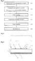
- the method for manufacturing a semiconductor substrate for a solar cell of the present invention corresponds to the step (F-3), and the step is shown in a process flowchart for forming an irregularity structure in Fig. 2.
- the silicon substrate sliced in the previous step (F-2) is usually treated with an aqueous acidic solution or an aqueous alkaline solution to remove a fracture layer (residues from slicing) on the substrate surface chemically.
- the removed thickness which depends on conditions for the slicing, is generally from 5 to 20 ⁇ m.
- the method for manufacturing a semiconductor substrate for a solar cell of the present invention can be applied thereto.
- an acidic solution (containing silver or copper) is manufactured (prepared) (G-1).
- Fig. 2 shows a case of the silver-containing solution.
- the acidic solution is a solution containing silver ions or copper ions, fluoride ions, and nitrate ions.
- the acidic solution can be obtained by dissolving 60 cc of a 60% nitric acid solution and 0.5 g of pure silver powder into 2 liters of a 50% hydrofluoric acid solution at room temperature.
- the mol concentration of silver in the silver-containing solution ranges from 1 x 10 -6 to 1 x 10 -2 mol/L, preferably from 1 x 10 -5 to 1 x 10 -3 mol/L.
- the mass of copper should be about 2.5 times the mass of silver.
- the mol concentration of silver in the copper-containing solution ranges from 1 x 10 -6 to 1 x 10 -2 mol/L, preferably from 1 x 10 -5 to 1 x 10 -3 mol/L.
- the acidic solution is preferably an aqueous solution further containing one or more species selected from acetate ions, sulfate ions, and phosphate ions.
- the reaction rate is restrained so that irregularities can be formed in the surface of the semiconductor substrate with a good control.
- the viscosity of the aqueous solution becomes high so that the irregularity shapes formed in the surface of the semiconductor substrate can be made gentler. This causes an improvement in the contact resistance with electrodes formed by printing and firing.
- the semiconductor substrate is immersed in the resultant acidic solution to form a surface irregularity structure of the present invention in the semiconductor substrate (G-2).
- This step is an isotropic etching with an acid.
- the silicon substrate is immersed in the acidic solution for 5 minutes.
- the semiconductor substrate is taken out from the acidic solution, and then washed sufficiently with water (G-3).
- the silicon substrate taken out from the acidic solution is washed with water for about 3 minutes.
- the surface of the silicon substrate washed with water changes from silvery white, which is an original color of silicon, to black, which is optically high in light absorption.
- this layer is referred to as a "stain layer”, “stain film”, “silicon porous layer” or “porous layer”.
- the inventors of the present invention have observed the stain layer with an electron microscope. As a result, ascertained have been crepe-pattern irregularities wherein the width and the depth are each from 0.1 to 10 ⁇ m inwards from the surface of the silicon substrate.
- the semiconductor substrate is immersed in an alkaline solution to remove the stain layer (G-4).
- the alkaline solution is preferably an aqueous solution containing one or more selected from sodium hydroxide, potassium hydroxide, ammonium hydroxide, hydrazine, sodium carbonate and potassium carbonate.
- an aqueous sodium hydroxide solution is particularly preferable. It is advisable to set the conditions for the concentration of the solution, the immersion, and others appropriately. For example, the silicon substrate is immersed in a 10% aqueous solution of sodium hydroxide at room temperature. At this time, fine bubbles are generated from the silicon substrate surface. The reaction will be detailed later.
- This immersion makes it possible to remove projections having a height of about 0.1 ⁇ m or less, which block the conduction of electrons generated by light absorption.
- the semiconductor substrate is taken out from the alkaline solution after the generation of the bubbles stops.
- the semiconductor substrate is sufficiently washed with water (G-5).
- the silicon substrate taken out from the alkaline solution is washed with water for about 3 minutes.
- the alkaline solution adhering to the semiconductor substrate is neutralized with an acidic solution or the like (G-6). It is advisable to set conditions for the neutralization appropriately.
- the silicon substrate is immersed in a 1% or 10% aqueous solution of diluted hydrochloric acid to neutralize alkaline components in the silicon substrate surface.
- the silicon substrate surface is oxidized with nitric acid to produce SiO 2 , thereby generating nitrogen monoxide (NO).
- NO nitrogen monoxide
- Silver (Ag) deposited at this time reacts with nitric acid as described in the following formula, so as to turn immediately into silver nitrate, then silver ions.
- the silver ions in the solution are recycled, so that the concentration of the silver ions in the solution does not change.
- SiO 2 formed in the silicon surface according to the reaction (1) reacts with hydrogen fluoride (HF) as follows. SiO 2 + 4HF ⁇ SiF 4 ⁇ + H 2 O (4)
- Tetrafluorosilane (SiF 4 ) generated reacts with hydrogen fluoride to form complex ions (hexafluorosilanoate ions: SiF 6 2- ).
- Hexafluorosilanoic acid shows strong acidity, and is ionized in the aqueous solution at a far higher ratio than hydrofluoric acid (HF), which is a weak acid.
- the nitrate ion concentration in the acidic solution is preferably from 0.01 to 1 mol/L.
- SiO 2 formed in the silicon surface in the reaction (1) is immediately pulled off from the silicon surface through the reaction (4). At the same time, bubbles are generated. As shown in the reactions (1) to (5), the bubbles contain NO, NO 2 , H 2 and SiF 4 . When NO 2 in the bubbles and dissolved NO 2 in the solution are brought into contact with the silicon, the following reaction is caused. Si + 2NO 2 ⁇ SiO 2 + 2NO ⁇ (6)
- reaction (2) does not take place but the following reaction, wherein hydrogen ions (H + ) acts mainly, takes place.
- NO 2 is generated in the same manner as in the reaction (2).
- the number of molecules and ions concerned therewith is required to be larger than that in the reaction (2), and further the ratio of the generation thereof is lower since nitrogen monoxide (NO) is slightly soluble in water. Accordingly, the amount of generated NO 2 relative to the number of silicon atoms concerned with the reaction (1) also becomes smaller so that a reaction corresponding to the reaction (3) does not take place.
- the reaction (6) gives an effect for promoting the formation of an irregularity structure in the silicon substrate surface; when a larger amount of NO 2 is brought into contact with the silicon surface portion that is once scrapped off, the formation of the irregularity structure is further promoted.
- the generation of NO 2 has a rate-determining step of the reaction (7), the reaction possibility of which is low; therefore, an irregularity structure is far less formed, as compared with the case that silver ions are present.
- the following describes a principle of removing the stain layer with an alkaline solution.
- crepe-pattern irregularities wherein the width and the depth are each from about 0.1 to 20 ⁇ m are formed in the silicon substrate surface.
- a silicon porous layer having fine irregularities the sizes of which range from 1 to 100 nm is formed in the surface layer regions of the silicon substrate.
- This layer is a blackened layer, so that reflection thereon is hardly observed within a range of visible light wavelengths.
- This silicon porous layer blocks the conduction of electrons generated by light absorption; therefore, it is necessary to remove this layer from the surface in order to obtain a solar cell properties.
- silicon gets radicals. Therefore, even if concentrated nitric acid is used, the reaction (1), for which 4 nitric acid molecules per 3 silicon atoms are necessary, is hardly caused. However, at room temperature, silicon reacts with an alkali as follows. Si + 2OH + H 2 O ⁇ SiO 3 2- + 2H 2 (8)
- the hydroxide ion concentration in the acidic solution is preferably from 0.025 to 2.5 mol/L, more preferably from 0.1 to 1.0 mol/L.
- the silicon substrate surface from which the porous layer is removed has a surface irregularity structure wherein the surface area containing irregularities is from 1.2 to 2.2 times the surface area of the imaginary smooth face and the standard deviation of the heights of the irregularities is 1.0 ⁇ m or less; or a surface irregularity structure wherein aggregate sections of irregularities having irregularity heights ranging from 0.1 to 2 ⁇ m are mixed with sections having irregularity heights ranging from 5 to 20 ⁇ m.
- the reflectivity, including scattered light is 15% or less within a wavelength range from 500 to 1000 nm.
- Any silicon substrate having such a surface irregularity structure acts normally and is electrically stable even if a pn junction is formed in its surface by phosphorus diffusion or the like.
- a solar cell manufactured by use of a semiconductor substrate for a solar cell manufactured by the above-mentioned method has an irregularity structure having good properties, and is low in reflectivity and high in efficiency.
- the resultant square pole was sliced into a thickness of 300 ⁇ m with a wire saw to obtain 200 polycrystalline silicon substrates.
- the pole was cut into four out of the 200 polycrystalline silicon substrates, the four substrates were successively separated into 4 groups.
- group A, groups B, group C and group Z were obtained, in each of which the number of the substrates was 50.
- the polycrystalline silicon substrates of the respective obtained groups were washed by the RCA method.
- the polycrystalline silicon substrates of groups A and B were each immersed in a solution wherein a 60% nitric acid solution and a 50% hydrofluoric acid solution were mixed at 3/1 for 1 minute, so as to be etched into a depth of about 10 ⁇ m, thereby removing a damaged layer generated by the slicing.
- the polycrystalline silicon substrates of groups A and B were each immersed in a 10% aqueous solution of sodium hydroxide at room temperature. Fine bubbles were generated from the surface of the polycrystalline silicon substrate during the immersion. After the generation of the bubbles stopped, the polycrystalline silicon substrate was taken out from the aqueous solution of sodium hydroxide, and washed with pure water for 5 minutes. Thereafter, the polycrystalline silicon substrate was immersed in a 10% aqueous solution of diluted hydrochloric acid for 5 minutes to neutralize the alkaline component on the substrate surface. The resultant was again washed with pure water for 3 minutes, and dried.
- the isotropic texturing device manufactured by RENA Sondermaschinen GMBH was used to form irregularities in each of the surfaces of the polycrystalline silicon substrates of group C by a method recommended by this company.
- Irregularities were formed in each of the surfaces of the polycrystalline silicon substrates of group Z by alkali etching, which is widely used to form irregularities in single crystalline silicon substrates.
- the polycrystalline silicon substrates were each immersed in a 3% aqueous solution of sodium hydroxide, having a temperature of 85 to 90°C, for 20 minutes, and further immersed in a 10% aqueous solution of diluted hydrochloric acid for 10 minutes to neutralize the alkaline component on the substrate surface, thereby forming irregularities in the substrate surface.
- the "surface area containing irregularities" and the "standard deviation of the heights of the irregularities” of each of the semiconductor substrates were measured by use of a confocal laser scanning microscope using a semiconductor laser light having a wavelength of 408 nm, such as a microscope, model No. LEXT OLS3000, manufactured by Olympus Corporation. Specifically, from the surface of the semiconductor substrate, 16 points were selected at will.
- the above-mentioned microscope with an objective lens of 100 magnifications was used under 1-power optical zooming in an enhancing mode to take in height data on its surface irregularities in a step search manner at a height resolving power of 0.01 ⁇ m.
- the resultant height data on the irregularities were subjected to smoothing correction one time along an XY direction in a median mode with a mask size of 5. In this way, measurement noises were removed.
- the "surface area containing irregularities” and the "surface area of the imaginary smooth face” were obtained, and in accordance with a surface roughness menu, the "standard deviation (SRq) of the heights of the irregularities” was obtained. These operations were repeated about the 16 measured points.
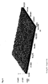
- Figs. 5 to 7 are graphics showing the typical bird's eye observation images of the surfaces of the polycrystalline silicon substrates of group A, group B and group C, respectively.
- Table 1 Group Method Short circuit current (A) Open Circuit current (V) Fill factor (%) Conversion efficiency (%) Surface area/base area Standard deviation of heights ( ⁇ m) A Silver ions 3.18 0.614 77.5 15.1 1.44 0.45 B Copper ions 3.16 0.613 77.2 15.0 1.35 0.50 C RENA GMBH 3.17 0.609 75.8 14.6 1.47 1.40 Z Alkali 3.09 0.613 74.9 14.2 1.17 0.89
- the polycrystalline silicon substrates of groups A, B and C are each have a surface area 1.4 times the base area so as to exhibit an excellent effect of preventing light reflection, and thus similar short circuit currents are obtained.
- each of the polycrystalline silicon substrates of group C has larger irregularity undulations on its surfaces.
- steps that cannot be neglected are generated, in the direction along which electric current flows, in the electrodes.
- the electric resistance somewhat increases.
- the solar cells of groups A and B have a better fill factor and give a higher conversion efficiency than the solar cells of group C.
- the ratio of the surface area to the base area, and the standard deviation of the heights each exhibit a large scattering, depending on locations, and thus the effect of preventing light reflection is insufficient. Furthermore, the steps of the electrodes are large in number, and thus the electric resistance increases and the fill factor becomes a low value.
- Example 2 250 polycrystalline silicon substrates were obtained. Whenever five out of the 250 polycrystalline silicon substrates was cut off, the five substrates were successively separated into 5 groups. Thus, group A, group D, group E, group F and group Z were obtained, in each of which the number of the substrates was 50. The polycrystalline silicon substrates of the resultant respective groups were washed by the RCA method.
- the polycrystalline silicon substrates of groups A, D, E and F were each immersed in a solution wherein a 60% nitric acid solution and a 50% hydrofluoric acid solution were mixed at 3/1 for 1 minute, so as to be etched into a depth of about 10 ⁇ m, thereby removing a damaged layer generated by the slicing.
- the present invention is concerned with Japanese Patent Application No. 2004-159721 filed on May 28, 2004 , and the present application therefor is filed with a priority claim thereof. The content thereof is incorporated herein for reference.
Landscapes
- Photovoltaic Devices (AREA)
- Weting (AREA)
Applications Claiming Priority (2)
| Application Number | Priority Date | Filing Date | Title |
|---|---|---|---|
| JP2004159721 | 2004-05-28 | ||
| PCT/JP2005/009675 WO2005117138A1 (ja) | 2004-05-28 | 2005-05-26 | 太陽電池用半導体基板とその製造方法および太陽電池 |
Publications (1)
| Publication Number | Publication Date |
|---|---|
| EP1753032A1 true EP1753032A1 (de) | 2007-02-14 |
Family
ID=35451161
Family Applications (1)
| Application Number | Title | Priority Date | Filing Date |
|---|---|---|---|
| EP05743744A Withdrawn EP1753032A1 (de) | 2004-05-28 | 2005-05-26 | Halbleitersubstrat für eine solarzelle, herstellungsverfahren dafür und solarzelle |
Country Status (5)
| Country | Link |
|---|---|
| US (1) | US20090038682A1 (de) |
| EP (1) | EP1753032A1 (de) |
| JP (1) | JPWO2005117138A1 (de) |
| CN (1) | CN100472817C (de) |
| WO (1) | WO2005117138A1 (de) |
Cited By (3)
| Publication number | Priority date | Publication date | Assignee | Title |
|---|---|---|---|---|
| WO2009119995A3 (en) * | 2008-03-26 | 2009-12-10 | Lg Electronics Inc. | Method of texturing solar cell and method of manufacturing solar cell |
| EP2182556A4 (de) * | 2007-10-24 | 2011-05-18 | Mitsubishi Electric Corp | Prozess zum herstellen einer solarzelle |
| EP2551915A1 (de) * | 2011-07-29 | 2013-01-30 | LG Electronics Inc. | Solarzelle |
Families Citing this family (15)
| Publication number | Priority date | Publication date | Assignee | Title |
|---|---|---|---|---|
| NL2000248C2 (nl) * | 2006-09-25 | 2008-03-26 | Ecn Energieonderzoek Ct Nederl | Werkwijze voor het vervaardigen van kristallijn-silicium zonnecellen met een verbeterde oppervlaktepassivering. |
| KR101494153B1 (ko) | 2007-12-21 | 2015-02-23 | 주성엔지니어링(주) | 박막형 태양전지 및 그 제조방법 |
| KR20100124660A (ko) * | 2009-05-19 | 2010-11-29 | 주성엔지니어링(주) | 태양전지 및 그의 제조방법 |
| CN102181936A (zh) * | 2010-10-26 | 2011-09-14 | 江阴浚鑫科技有限公司 | 一种制作多晶硅绒面的方法及腐蚀液 |
| JP5921091B2 (ja) * | 2011-06-03 | 2016-05-24 | 林純薬工業株式会社 | エッチング液組成物およびエッチング方法 |
| JP5715509B2 (ja) * | 2011-06-22 | 2015-05-07 | シャープ株式会社 | 太陽電池、及び太陽電池の製造方法 |
| JP5912538B2 (ja) * | 2012-01-10 | 2016-04-27 | 株式会社半導体エネルギー研究所 | シリコンからなる半導体基板および光電変換装置 |
| CN102646758A (zh) * | 2012-05-05 | 2012-08-22 | 云南师范大学 | 一种太阳电池用单晶硅片表面改性方法 |
| WO2013180221A1 (ja) * | 2012-05-31 | 2013-12-05 | 日本化成株式会社 | 太陽電池用シリコンウエハー及びその製造方法 |
| CN105142763B (zh) * | 2013-04-25 | 2019-11-12 | 索尔维公司 | 用于纯化氢氟酸和硝酸的混合物的反渗透 |
| CN103346209B (zh) * | 2013-06-24 | 2016-02-17 | 陕西师范大学 | 用于增强太阳光利用率的表面修饰基材的修饰方法 |
| CN105576074A (zh) * | 2014-10-08 | 2016-05-11 | 上海神舟新能源发展有限公司 | 一种n型双面电池的湿法刻蚀方法 |
| CN105671641A (zh) * | 2014-11-20 | 2016-06-15 | 日本化成株式会社 | 太阳能电池用硅晶片的制造方法 |
| CN105220235B (zh) * | 2015-10-12 | 2017-12-08 | 常州捷佳创精密机械有限公司 | 一种单多晶制绒方法 |
| CN105870263B (zh) * | 2016-06-27 | 2018-07-31 | 苏州阿特斯阳光电力科技有限公司 | 一种晶体硅太阳能电池绒面结构的制备方法 |
Family Cites Families (15)
| Publication number | Priority date | Publication date | Assignee | Title |
|---|---|---|---|---|
| US4431858A (en) * | 1982-05-12 | 1984-02-14 | University Of Florida | Method of making quasi-grain boundary-free polycrystalline solar cell structure and solar cell structure obtained thereby |
| JPH07105518B2 (ja) * | 1989-08-10 | 1995-11-13 | シャープ株式会社 | 光電変換装置用基板の加工方法 |
| FR2741194B1 (fr) * | 1995-11-13 | 1998-01-30 | Photowatt Int | Cellule solaire comportant du silicium multicristallin et procede de texturisation de la surface du silicium multicristallin de type p |
| US5846522A (en) * | 1996-02-13 | 1998-12-08 | Kosti; Carl | Fluoridation and refluoridation of water based compositions |
| US5919311A (en) * | 1996-11-15 | 1999-07-06 | Memc Electronic Materials, Inc. | Control of SiO2 etch rate using dilute chemical etchants in the presence of a megasonic field |
| JP3772456B2 (ja) * | 1997-04-23 | 2006-05-10 | 三菱電機株式会社 | 太陽電池及びその製造方法、半導体製造装置 |
| JP2000332279A (ja) * | 1999-05-24 | 2000-11-30 | Kyocera Corp | 太陽電池の製造方法 |
| JP2001326370A (ja) * | 2000-05-12 | 2001-11-22 | Mitsubishi Electric Corp | 太陽電池の製造方法及びその太陽電池 |
| WO2002031892A1 (fr) * | 2000-10-06 | 2002-04-18 | Shin-Etsu Handotai Co., Ltd. | Cellule solaire et procede de fabrication correspondant |
| JP4340031B2 (ja) * | 2001-09-26 | 2009-10-07 | 京セラ株式会社 | 太陽電池用基板の粗面化方法 |
| AU2003242229A1 (en) * | 2002-06-06 | 2003-12-22 | Kansai Technology Licensing Organization Co., Ltd. | Method for producing polycrystalline silicon substrate for solar cell |
| JP2004172271A (ja) * | 2002-11-19 | 2004-06-17 | Mitsubishi Electric Corp | 太陽電池の製造方法及び太陽電池 |
| JP2004235274A (ja) * | 2003-01-28 | 2004-08-19 | Kyocera Corp | 多結晶シリコン基板およびその粗面化法 |
| JP3925867B2 (ja) * | 2003-12-17 | 2007-06-06 | 関西ティー・エル・オー株式会社 | 多孔質層付きシリコン基板を製造する方法 |
| JP7105518B2 (ja) * | 2020-10-16 | 2022-07-25 | 株式会社トライフォース・マネジメント | 力覚センサ |
-
2005
- 2005-05-26 WO PCT/JP2005/009675 patent/WO2005117138A1/ja not_active Ceased
- 2005-05-26 CN CNB2005800171860A patent/CN100472817C/zh not_active Expired - Fee Related
- 2005-05-26 JP JP2006513946A patent/JPWO2005117138A1/ja active Pending
- 2005-05-26 US US11/597,425 patent/US20090038682A1/en not_active Abandoned
- 2005-05-26 EP EP05743744A patent/EP1753032A1/de not_active Withdrawn
Non-Patent Citations (1)
| Title |
|---|
| See references of WO2005117138A1 * |
Cited By (11)
| Publication number | Priority date | Publication date | Assignee | Title |
|---|---|---|---|---|
| EP2182556A4 (de) * | 2007-10-24 | 2011-05-18 | Mitsubishi Electric Corp | Prozess zum herstellen einer solarzelle |
| US8119438B2 (en) | 2007-10-24 | 2012-02-21 | Mitsubishi Electric Corporation | Method of manufacturing solar cell |
| WO2009119995A3 (en) * | 2008-03-26 | 2009-12-10 | Lg Electronics Inc. | Method of texturing solar cell and method of manufacturing solar cell |
| US7858426B2 (en) | 2008-03-26 | 2010-12-28 | Lg Electronics Inc. | Method of texturing solar cell and method of manufacturing solar cell |
| KR101168589B1 (ko) | 2008-03-26 | 2012-07-30 | 엘지전자 주식회사 | 계면 활성제를 이용한 실리콘 태양전지의 텍스처링 방법 |
| US8232128B2 (en) | 2008-03-26 | 2012-07-31 | Lg Electronics Inc. | Method of texturing solar cell and method of manufacturing solar cell |
| EP2551915A1 (de) * | 2011-07-29 | 2013-01-30 | LG Electronics Inc. | Solarzelle |
| CN102903768A (zh) * | 2011-07-29 | 2013-01-30 | Lg电子株式会社 | 太阳能电池 |
| US9166082B2 (en) | 2011-07-29 | 2015-10-20 | Lg Electronics Inc. | Solar cell |
| CN102903768B (zh) * | 2011-07-29 | 2015-11-25 | Lg电子株式会社 | 太阳能电池 |
| US9412885B2 (en) | 2011-07-29 | 2016-08-09 | Lg Electronics Inc. | Solar cell |
Also Published As
| Publication number | Publication date |
|---|---|
| CN100472817C (zh) | 2009-03-25 |
| JPWO2005117138A1 (ja) | 2008-04-03 |
| CN1961430A (zh) | 2007-05-09 |
| WO2005117138A1 (ja) | 2005-12-08 |
| US20090038682A1 (en) | 2009-02-12 |
Similar Documents
| Publication | Publication Date | Title |
|---|---|---|
| EP1753032A1 (de) | Halbleitersubstrat für eine solarzelle, herstellungsverfahren dafür und solarzelle | |
| EP2182556B1 (de) | Verfahren zum Herstellen einer Solarzelle | |
| AU2005264235B2 (en) | Electrode material, solar cell and process for producing solar cell | |
| US9583652B2 (en) | Method for the wet-chemical etching back of a solar cell emitter | |
| US11251318B2 (en) | Efficient black silicon photovoltaic devices with enhanced blue response | |
| JP6435340B2 (ja) | 結晶シリコン系太陽電池の製造方法、及び太陽電池モジュールの製造方法 | |
| JP2003258285A (ja) | 表面凹凸構造の作製方法及び太陽電池 | |
| EP1936698A1 (de) | Herstellungsverfahren für Solarzellen | |
| JP4766880B2 (ja) | 結晶シリコンウエハ、結晶シリコン太陽電池、結晶シリコンウエハの製造方法および結晶シリコン太陽電池の製造方法 | |
| KR20080014751A (ko) | 태양전지의 제조 방법 및 태양전지 | |
| KR20140010155A (ko) | 태양 전지용 웨이퍼의 제조방법, 태양 전지 셀의 제조방법, 및 태양 전지 모듈의 제조방법 | |
| Ju et al. | A new vapor texturing method for multicrystalline silicon solar cell applications | |
| Sreejith et al. | A low cost additive-free acid texturing process for large area commercial diamond-wire-sawn multicrystalline silicon solar cells | |
| JP5509410B2 (ja) | 太陽電池用シリコン基板の製造方法 | |
| JP5408022B2 (ja) | 太陽電池セル及びその製造方法 | |
| CN119452759A (zh) | 带纹理表面的生成、串联太阳能电池的制造以及串联太阳能电池 | |
| KR101642045B1 (ko) | 태양전지용 웨이퍼, 태양전지용 웨이퍼의 제조 방법, 태양전지 셀의 제조 방법, 및 태양전지 모듈의 제조 방법 | |
| KR101528864B1 (ko) | 태양전지용 웨이퍼 및 그 제조 방법 | |
| JP3602323B2 (ja) | 太陽電池の製造方法 | |
| JP2005340643A (ja) | 太陽電池用半導体基板の製造方法 | |
| JP2005136062A (ja) | 太陽電池の製造方法 | |
| JP5724718B2 (ja) | 太陽電池用ウェーハの製造方法、太陽電池セルの製造方法、および太陽電池モジュールの製造方法 | |
| JP2005327871A (ja) | 太陽電池及びその製造方法 | |
| Li et al. | Facile fabrication of Si nanowire arrays for solar cell application |
Legal Events
| Date | Code | Title | Description |
|---|---|---|---|
| PUAI | Public reference made under article 153(3) epc to a published international application that has entered the european phase |
Free format text: ORIGINAL CODE: 0009012 |
|
| 17P | Request for examination filed |
Effective date: 20061120 |
|
| AK | Designated contracting states |
Kind code of ref document: A1 Designated state(s): DE ES FR IT |
|
| DAX | Request for extension of the european patent (deleted) | ||
| RBV | Designated contracting states (corrected) |
Designated state(s): DE ES FR IT |
|
| STAA | Information on the status of an ep patent application or granted ep patent |
Free format text: STATUS: THE APPLICATION HAS BEEN WITHDRAWN |
|
| 18W | Application withdrawn |
Effective date: 20130328 |