EP1754809A2 - Monocristaux volumineux et orientés présentant un indice de réfraction homogène et une faible biréfringence par compression - Google Patents
Monocristaux volumineux et orientés présentant un indice de réfraction homogène et une faible biréfringence par compression Download PDFInfo
- Publication number
- EP1754809A2 EP1754809A2 EP06023376A EP06023376A EP1754809A2 EP 1754809 A2 EP1754809 A2 EP 1754809A2 EP 06023376 A EP06023376 A EP 06023376A EP 06023376 A EP06023376 A EP 06023376A EP 1754809 A2 EP1754809 A2 EP 1754809A2
- Authority
- EP
- European Patent Office
- Prior art keywords
- crystal
- melt
- temperature
- heating
- crucible
- Prior art date
- Legal status (The legal status is an assumption and is not a legal conclusion. Google has not performed a legal analysis and makes no representation as to the accuracy of the status listed.)
- Withdrawn
Links
- 239000013078 crystal Substances 0.000 title claims abstract description 123
- 238000010438 heat treatment Methods 0.000 claims abstract description 59
- 239000000155 melt Substances 0.000 claims abstract description 28
- 230000008018 melting Effects 0.000 claims description 49
- 238000002844 melting Methods 0.000 claims description 49
- 239000002994 raw material Substances 0.000 claims description 14
- 230000005501 phase interface Effects 0.000 claims description 11
- 238000002425 crystallisation Methods 0.000 claims description 9
- 230000008025 crystallization Effects 0.000 claims description 9
- 239000007787 solid Substances 0.000 claims description 6
- 239000007788 liquid Substances 0.000 claims description 3
- 229910016036 BaF 2 Inorganic materials 0.000 claims description 2
- 229910004261 CaF 2 Inorganic materials 0.000 claims description 2
- 230000017525 heat dissipation Effects 0.000 claims description 2
- 230000001747 exhibiting effect Effects 0.000 claims 1
- 238000000034 method Methods 0.000 abstract description 37
- 230000008569 process Effects 0.000 abstract description 11
- 239000007791 liquid phase Substances 0.000 abstract description 3
- 239000007790 solid phase Substances 0.000 abstract description 3
- 238000005452 bending Methods 0.000 abstract 1
- 238000001816 cooling Methods 0.000 description 15
- OKTJSMMVPCPJKN-UHFFFAOYSA-N Carbon Chemical compound [C] OKTJSMMVPCPJKN-UHFFFAOYSA-N 0.000 description 13
- 229910002804 graphite Inorganic materials 0.000 description 12
- 239000010439 graphite Substances 0.000 description 12
- 238000004519 manufacturing process Methods 0.000 description 11
- 239000012071 phase Substances 0.000 description 10
- 230000003287 optical effect Effects 0.000 description 8
- 239000000463 material Substances 0.000 description 7
- 238000000265 homogenisation Methods 0.000 description 5
- 239000007789 gas Substances 0.000 description 4
- 239000012535 impurity Substances 0.000 description 4
- 239000011261 inert gas Substances 0.000 description 4
- 239000011810 insulating material Substances 0.000 description 4
- 238000009413 insulation Methods 0.000 description 4
- 230000005855 radiation Effects 0.000 description 4
- XLYOFNOQVPJJNP-UHFFFAOYSA-N water Substances O XLYOFNOQVPJJNP-UHFFFAOYSA-N 0.000 description 4
- WUKWITHWXAAZEY-UHFFFAOYSA-L calcium difluoride Chemical compound [F-].[F-].[Ca+2] WUKWITHWXAAZEY-UHFFFAOYSA-L 0.000 description 3
- 229910001634 calcium fluoride Inorganic materials 0.000 description 3
- 239000012212 insulator Substances 0.000 description 3
- 239000000203 mixture Substances 0.000 description 3
- IJGRMHOSHXDMSA-UHFFFAOYSA-N Atomic nitrogen Chemical compound N#N IJGRMHOSHXDMSA-UHFFFAOYSA-N 0.000 description 2
- -1 SrF 2 Inorganic materials 0.000 description 2
- QVGXLLKOCUKJST-UHFFFAOYSA-N atomic oxygen Chemical compound [O] QVGXLLKOCUKJST-UHFFFAOYSA-N 0.000 description 2
- 239000003990 capacitor Substances 0.000 description 2
- 230000008859 change Effects 0.000 description 2
- 239000012774 insulation material Substances 0.000 description 2
- 238000001459 lithography Methods 0.000 description 2
- 239000001301 oxygen Substances 0.000 description 2
- 229910052760 oxygen Inorganic materials 0.000 description 2
- 230000002028 premature Effects 0.000 description 2
- 230000001681 protective effect Effects 0.000 description 2
- 239000000126 substance Substances 0.000 description 2
- 235000012431 wafers Nutrition 0.000 description 2
- 229910000851 Alloy steel Inorganic materials 0.000 description 1
- 229910052582 BN Inorganic materials 0.000 description 1
- PZNSFCLAULLKQX-UHFFFAOYSA-N Boron nitride Chemical compound N#B PZNSFCLAULLKQX-UHFFFAOYSA-N 0.000 description 1
- 229910004573 CdF 2 Inorganic materials 0.000 description 1
- 229910001209 Low-carbon steel Inorganic materials 0.000 description 1
- 229910008449 SnF 2 Inorganic materials 0.000 description 1
- 238000000137 annealing Methods 0.000 description 1
- 230000005540 biological transmission Effects 0.000 description 1
- 230000015572 biosynthetic process Effects 0.000 description 1
- 238000009395 breeding Methods 0.000 description 1
- 230000001488 breeding effect Effects 0.000 description 1
- 238000012364 cultivation method Methods 0.000 description 1
- 238000000354 decomposition reaction Methods 0.000 description 1
- 230000007547 defect Effects 0.000 description 1
- 210000003298 dental enamel Anatomy 0.000 description 1
- 238000000151 deposition Methods 0.000 description 1
- 238000009792 diffusion process Methods 0.000 description 1
- 238000001704 evaporation Methods 0.000 description 1
- 239000002657 fibrous material Substances 0.000 description 1
- 230000004907 flux Effects 0.000 description 1
- 239000003779 heat-resistant material Substances 0.000 description 1
- 238000009776 industrial production Methods 0.000 description 1
- 238000011031 large-scale manufacturing process Methods 0.000 description 1
- 230000002045 lasting effect Effects 0.000 description 1
- 229910052757 nitrogen Inorganic materials 0.000 description 1
- 238000013021 overheating Methods 0.000 description 1
- 230000001590 oxidative effect Effects 0.000 description 1
- 238000000206 photolithography Methods 0.000 description 1
- 229920002120 photoresistant polymer Polymers 0.000 description 1
- 239000004033 plastic Substances 0.000 description 1
- 238000010926 purge Methods 0.000 description 1
- 239000002516 radical scavenger Substances 0.000 description 1
- 238000001953 recrystallisation Methods 0.000 description 1
- 230000009467 reduction Effects 0.000 description 1
- 239000000523 sample Substances 0.000 description 1
- 238000010583 slow cooling Methods 0.000 description 1
- 238000007711 solidification Methods 0.000 description 1
- 230000008023 solidification Effects 0.000 description 1
- 239000010935 stainless steel Substances 0.000 description 1
- 229910001220 stainless steel Inorganic materials 0.000 description 1
- 239000007858 starting material Substances 0.000 description 1
- 230000007704 transition Effects 0.000 description 1
- 238000002604 ultrasonography Methods 0.000 description 1
- 238000013022 venting Methods 0.000 description 1
- 210000002268 wool Anatomy 0.000 description 1
Images


Classifications
-
- C—CHEMISTRY; METALLURGY
- C30—CRYSTAL GROWTH
- C30B—SINGLE-CRYSTAL GROWTH; UNIDIRECTIONAL SOLIDIFICATION OF EUTECTIC MATERIAL OR UNIDIRECTIONAL DEMIXING OF EUTECTOID MATERIAL; REFINING BY ZONE-MELTING OF MATERIAL; PRODUCTION OF A HOMOGENEOUS POLYCRYSTALLINE MATERIAL WITH DEFINED STRUCTURE; SINGLE CRYSTALS OR HOMOGENEOUS POLYCRYSTALLINE MATERIAL WITH DEFINED STRUCTURE; AFTER-TREATMENT OF SINGLE CRYSTALS OR A HOMOGENEOUS POLYCRYSTALLINE MATERIAL WITH DEFINED STRUCTURE; APPARATUS THEREFOR
- C30B11/00—Single-crystal growth by normal freezing or freezing under temperature gradient, e.g. Bridgman-Stockbarger method
- C30B11/003—Heating or cooling of the melt or the crystallised material
-
- C—CHEMISTRY; METALLURGY
- C30—CRYSTAL GROWTH
- C30B—SINGLE-CRYSTAL GROWTH; UNIDIRECTIONAL SOLIDIFICATION OF EUTECTIC MATERIAL OR UNIDIRECTIONAL DEMIXING OF EUTECTOID MATERIAL; REFINING BY ZONE-MELTING OF MATERIAL; PRODUCTION OF A HOMOGENEOUS POLYCRYSTALLINE MATERIAL WITH DEFINED STRUCTURE; SINGLE CRYSTALS OR HOMOGENEOUS POLYCRYSTALLINE MATERIAL WITH DEFINED STRUCTURE; AFTER-TREATMENT OF SINGLE CRYSTALS OR A HOMOGENEOUS POLYCRYSTALLINE MATERIAL WITH DEFINED STRUCTURE; APPARATUS THEREFOR
- C30B11/00—Single-crystal growth by normal freezing or freezing under temperature gradient, e.g. Bridgman-Stockbarger method
-
- C—CHEMISTRY; METALLURGY
- C30—CRYSTAL GROWTH
- C30B—SINGLE-CRYSTAL GROWTH; UNIDIRECTIONAL SOLIDIFICATION OF EUTECTIC MATERIAL OR UNIDIRECTIONAL DEMIXING OF EUTECTOID MATERIAL; REFINING BY ZONE-MELTING OF MATERIAL; PRODUCTION OF A HOMOGENEOUS POLYCRYSTALLINE MATERIAL WITH DEFINED STRUCTURE; SINGLE CRYSTALS OR HOMOGENEOUS POLYCRYSTALLINE MATERIAL WITH DEFINED STRUCTURE; AFTER-TREATMENT OF SINGLE CRYSTALS OR A HOMOGENEOUS POLYCRYSTALLINE MATERIAL WITH DEFINED STRUCTURE; APPARATUS THEREFOR
- C30B29/00—Single crystals or homogeneous polycrystalline material with defined structure characterised by the material or by their shape
- C30B29/10—Inorganic compounds or compositions
- C30B29/12—Halides
-
- Y—GENERAL TAGGING OF NEW TECHNOLOGICAL DEVELOPMENTS; GENERAL TAGGING OF CROSS-SECTIONAL TECHNOLOGIES SPANNING OVER SEVERAL SECTIONS OF THE IPC; TECHNICAL SUBJECTS COVERED BY FORMER USPC CROSS-REFERENCE ART COLLECTIONS [XRACs] AND DIGESTS
- Y10—TECHNICAL SUBJECTS COVERED BY FORMER USPC
- Y10S—TECHNICAL SUBJECTS COVERED BY FORMER USPC CROSS-REFERENCE ART COLLECTIONS [XRACs] AND DIGESTS
- Y10S117/00—Single-crystal, oriented-crystal, and epitaxy growth processes; non-coating apparatus therefor
- Y10S117/90—Apparatus characterized by composition or treatment thereof, e.g. surface finish, surface coating
-
- Y—GENERAL TAGGING OF NEW TECHNOLOGICAL DEVELOPMENTS; GENERAL TAGGING OF CROSS-SECTIONAL TECHNOLOGIES SPANNING OVER SEVERAL SECTIONS OF THE IPC; TECHNICAL SUBJECTS COVERED BY FORMER USPC CROSS-REFERENCE ART COLLECTIONS [XRACs] AND DIGESTS
- Y10—TECHNICAL SUBJECTS COVERED BY FORMER USPC
- Y10T—TECHNICAL SUBJECTS COVERED BY FORMER US CLASSIFICATION
- Y10T117/00—Single-crystal, oriented-crystal, and epitaxy growth processes; non-coating apparatus therefor
- Y10T117/10—Apparatus
Definitions
- the invention relates to a method for growing large-volume single crystals of uniform orientation from a melt, to an apparatus for carrying out this method and to the use of crystals produced in this way.
- Single crystals are characterized by having a uniform orientation over their entire volume, which is a prerequisite for high optical homogeneity in the entire crystal volume. For this reason, they are outstandingly suitable for use in the optical industry or as a starting material for optical components in DUV photolithography as well as for stepper or excimer laser.
- Crystal Growth describes the most varied methods for growing crystals, of which the most frequent techniques are briefly mentioned below.
- crystals can be grown from the gas phase, the melt, from solutions or even from a solid phase by recrystallization or solid-state diffusion.
- these are usually intended only for the laboratory scale and not suitable for large-scale industrial production.
- the main commercial melt-growing processes for the production of crystals will be briefly explained below.
- a slightly cooled seed crystal is dipped in a crucible with molten crystal raw material by means of a finger and slowly pulled out, preferably under rotation. It grows when pulling out a larger crystal.
- This method has the disadvantage that relatively large temperature changes are produced by the cooling on the crystal, which lead to a stress-induced anisotropy.
- a crucible is melted in a mobile crucible by means of a heating mantle, and then the crucible is slowly lowered from the mantle in an axial temperature gradient established by the heater, or alternatively a movable heater re-establishes with the crucible stationary shifted above, with the melt cools and a seed added slowly grows.
- the so-called Bridgman Stockbager method the movable crucible is slowly lowered to form a crystal in an axial gradient between two superposed heating jackets, between which a sharp temperature step is formed.
- VVF method In the so-called vertical gradient freeze method (VGF method), a plurality of concentric heating circuits arranged one above the other are arranged in the form of a jacket around the stationary crucible. Each of these heating circuits can be controlled separately. By slowly shutting down the heating power of each individual heating circuit arranged around the crucible wall, the temperature can be slowly reduced below the crystallization point, whereby a radial temperature gradient occurs, along which crystal growth takes place.
- GSM gradient solidification method
- oriented single crystals usually do not show homogeneous optical and mechanical properties. It is desirable to form such crystals with a crystal orientation suitable for the particular use. However, this poses particular problems in the production of large single crystals, as these spontaneously give orientation in their culture, i. Change the position of the crystal axis, resulting in optically inhomogeneous crystals in which the refraction of light is not the same in all areas.
- the invention therefore has for its object to provide such large-volume crystals, which are in any chosen Adjustment along their ⁇ h, k, l axes ⁇ are preferably grown in the ⁇ 111 ⁇ or ⁇ 112 ⁇ orientation.
- a further object of the invention is to provide such large-volume crystals which extend far in all three spatial directions.
- the melting vessel is preferably round. In special cases, however, it may also be expedient for the melting vessel to have an oval or quadrangular cross section.
- the melting vessel comprises an inner receiving space, or melting space, which is formed by the melting vessel bottom, side walls and an upper opening opposite the bottom.
- the bottom opening opposite the upper opening is closed by a cover.
- the cover is preferably designed such that it does not rest gas-tight on the side walls, but leaves emerging during the melting evaporating impurities from the melting or crystal space.
- the cover is preferably designed such that it does not rest gas-tight on the side walls, but leaves emerging during the melting evaporating impurities from the melting or crystal space.
- the lateral elements are heat insulators, in particular those of heat-insulating material.
- the inventive device has a laterally spaced from the crucible support heating, which should prevent lateral heat flow. Conveniently, this support heater is arranged at a distance from the melting vessel, which is sufficient so that their heat generated can exert no direct influence on the processes in the melt.
- the support heater serves only to possibly, between the crucible and the surrounding, heat flow preventing elements and the environment occurring temperature gradients compensate. It is therefore usually spaced from the walls of the crucible by an intermediate layer of thermal insulation elements.
- the support heater is designed as a jacket heater.
- the bottom of the melting vessel can be configured as desired. Usually, however, it is lowered cone-shaped. He forms a pyramid or preferably a cone, with truncated pyramids or cones are particularly preferred.
- the bottom of the crucible preferably has a downwardly exiting pocket, which serves to receive a seed or seed crystal with a predetermined orientation.
- the germ pocket is preferably in the middle of the bottom, i. arranged on the cone or pyramid tip.
- the germ pocket has a cooling element, in particular at its lower end. This cooling element is preferably a water-filled cooling element, which protects the seed crystal present in the seed bag from being prematurely on or melted during melting of the crystal raw material.
- the cooling element is heatable.
- the crucible on an above the melting chamber arranged expanded buffer space, which serves as a funnel for filling the crystal raw material.
- it serves to equilibrate the amount of heat emitted by a cover heater, so that a uniformly acting on the crystal mass heat flow is generated and possibly resulting from the heating local temperature differences are compensated.
- the actual melting chamber is provided with a heat-conducting cover which separates the insulation space and the actual melting space. It also serves to equilibrate the temperature and consists of a material that is only slightly insulating or insulating.
- the device according to the invention now has at least one heating element arranged above the melting vessel.
- a lateral heat flow preventing insulating element is formed by heating this above the melting vessel arranged heating element, in the melting vessel exclusively axially extending heat flow.
- a lateral heat flow is prevented by the insulation elements.
- This upper heating element is expediently a lid heater.
- the bottom heating is arranged below the bottom of the crucible so that it does not include the seed bag or at least with respect to this insulating spaced to avoid premature unwanted melting of the crystal nucleus / seed crystal.
- all the heating elements are enclosed in an envelope of insulating material surrounding the melting vessel in order to avoid unwanted and uncontrolled heat flow in this way.
- the one or more temperature-measuring elements are / is formed as a sliding element, which are mounted slidably from the outside during operation of the device along the side wall so as to measure the temperature gradient running axially from the vessel bottom to the vessel lid.
- Preferred measuring elements are thermocouples, thermistors and in particular pyrometers.
- the device according to the invention has a device with which the boundary between solid crystalline and molten liquid phase can be determined.
- a phase sensor has proven to be useful, which comprises a running in a hollow guide tube probe rod, which extends into the melting vessel and the rod in the guide tube can be lowered slowly down, wherein the solid crystalline phase is felt.
- the phase sensor consists of an ultrasound device, which dips into the melt from above and measures the sound waves reflected at the phase interface and in this way determines the crystal growth.
- the device has a capacitor which is arranged above the opening of the crucible and which separates any material vapors that escape.
- the housing of the device according to the invention comprises a closable and openable cover, via which the melting vessel can be charged with crystal raw material and the finished crystal can be removed.
- the housing of the device has at least one opening for venting the entire interior. About this opening, the interior of the device can be placed under vacuum and / or possibly filled with a protective gas.
- the arranged within the housing elements of the inventive device are preferably made of graphite.
- the melting vessel is formed from a good heat-conducting pressed graphite.
- the insulation material preferably consists of a loosely packed graphite, in particular fiber materials of graphite wool or graphite mats.
- the Heating elements are expediently formed from graphite, with heat-generating, electrically conductive graphite paths meander around the area to be heated and generate heat as current resistance heating. To avoid short circuits, the current-carrying elements are kept apart from the adjacent graphite parts by means of insulators.
- Preferred insulators are boron nitride.
- the housing of the system according to the invention usually consists of a chemically resistant, heat-resistant material and is preferably a steel alloy, with stainless steel being particularly preferred. However, in many cases also mild steel has been found to be sufficient.
- the invention also relates to a process for the production of large-volume single crystals.
- the procedure is such that melting a crystal raw material in a vessel having a bottom, lateral walls, an upper opening and, optionally, a cover which at least partially closes the upper opening.
- it is also possible to introduce the crystal raw material already in the molten state in the melting vessel.
- the procedure according to the invention is to slowly cool the melt from the bottom of the crucible towards the surface of the melt or cover heating above the melt surface, forming a crystal nucleus on the bottom of the vessel, which then travels along the temperature gradient or along the temperature gradient Heat flux axis grows.
- the procedure is such that only a heat flow or temperature gradient is formed between the vessel bottom and the melt surface or the cover or lid heater. This means that in the crucible superimposed temperature surfaces are formed which are flat, the temperature increases from the bottom of the crucible to the surface of the melt or lid heating, wherein within a temperature surface or temperature level at all points, the temperature is the same, ie ° C varies.
- the temperature increase between the vessel bottom and the surface of the melt is continuous. If the areas in which the temperature is the same have a minimal curvature, then their radius ⁇ 1 m. Radii> 2 m are particularly preferred, with radii> 4 m being particularly preferred.
- phase interface is formed between the solid crystalline and the liquid molten phases that propagate along the temperature profile, i. parallel to the planes of equal temperature and grows perpendicular to these planes.
- the necessary for the inventive crystal growth planar phase interface is achieved by avoiding a lateral, ie radial heat flow.
- This is achieved by means of lateral elements arranged in particular around the walls of the melting vessel.
- Such elements are preferably a support heater and / or an insulating material.
- spaced apart heating elements along the side walls, which serve exclusively for temperature support.
- the between the melting vessel and spaced heating which is preferably designed as a jacket heating, resulting gap filled with insulation material, which on the one hand prevents lateral heat dissipation and thus the formation of a radial temperature gradient and which on the other hand prevents the support heater generates local overheating in the melting vessel.
- the support heater is used in essential to counteract any heat losses through the insulation jacket and thus supports the radial leveling of the temperature profile.
- the seed crystal is preferably a monocrystal which is introduced into a seed pocket attached to the bottom of the vessel, preferably such that its orientation corresponds to the desired later orientation of the bulky single crystal.
- the procedure is then such that the crystal raw material present in the vessel is melted by heating the cover heating and preferably the bottom heating.
- the jacket heater is used here to assist.
- the crucible is preferably heated to a temperature at which any water of crystallization is released first. Thereafter, the temperature is further increased, optionally dissolved gases or gaseous parts bound in the crystal bulk mass, as well as formed by heating gaseous decomposition products, are released.
- the enamel is homogenized.
- This is achieved, in particular, by adjusting the heating power of the heating elements in such a way that convection occurs in the melt, as a result of which they are continuously mixed is so that dissolved and undesirable impurities reach the melt surface, where in particular quite volatile substances can evaporate.
- evaporated crystal material is deposited in a preferably cooled condenser.
- the homogenization of the melt is carried out for at least two days, but in particular for at least five days, at least one week being very particularly preferred.
- the seed present in the seed bag is preferably cooled in order to avoid premature melting or melting. This is usually done by means of a water cooling.
- the cooling is advantageously carried out by means of a water cooled graphite rod.
- the seed is carefully melted. This is usually done by reducing the cooling capacity and / or by employing a germ pocket heater.
- the seed crystal is carefully melted from top to bottom, resulting in a uniform transition between the seed and the melt.
- the axial temperature gradient is formed by either the heating power of the lid heater and / or the floor heating is slowly lowered.
- the procedure is such that the ceiling heating is adjusted to a temperature which is the same or above, preferably slightly above the crystallization temperature of the crystal to be produced.
- Appropriate lid heating temperatures are 200-300 ° C above the crystallization temperature.
- the temperature of the bottom heating is expediently at least 650 ° C., preferably at least 900 ° C., but is lower than the melting temperature in the case of crystal growth. Thereafter, the heating power of Floor heating slowly lowered. By moving the bottom heater down to a temperature below the crystallization temperature, the melt slowly cools down along the axial temperature gradient, the phase interface which forms at the plane of the crystallization temperature slowly shifts from top to bottom in the melting vessel, causing the crystal to grow. In principle, it is also possible to shut down the temperature of the lid heater. In this case, the temperature is reduced at a rate at which the crystal growth is 0.01 to 5 mm / hour, preferably 0.1 to 1 mm / hour and in particular 0.2 to 0.5 mm / hour. These values are usually achieved at a cooling rate of 0.001 to 5 ° C per hour.
- the lower cone-shaped bottom part of the crucible i. in the part that forms the bottom between the germ pocket and the crucible wall, at the beginning of crystal growth form a non-planar up to the lid curved phase interface having a radius ⁇ 1 m, preferably ⁇ 0.8 m, in particular ⁇ 0.5 m having.
- the crystal thus obtained is tempered.
- any existing crystalline inhomogeneities at elevated temperature are compensated, ie crystal defects are annealed at this temperature.
- the Whole large volume single crystal slowly cooled to room temperature.
- Such cooling is usually carried out over several days to several weeks and, depending on the phase and stage preferably with a cooling rate of about 0.001 ° C / hour to 15 ° C / hour, especially up to 10 ° C / hour and preferably to 1 ° C / hour, with 0.01 ° C / hour to 8 ° C / hour, especially 3 ° C / hour being preferred.
- Even when cooling a substantially axial temperature gradient is preferably maintained.
- the cooling rate is preferably controlled by means of a plurality of temperature sensors arranged in the device according to the invention. In this way, the temperature profile of the cooling can also regulate, which is carried out as well as in the crystal growth expediently by means of a computer.
- the crystal raw material used in the process according to the invention comprises, in particular, raw materials which, in addition to the crystal material, also contain scavengers which, in a homogenization phase, react with possibly present impurities to form readily volatile substances.
- Preferred crystal materials are MgF 2 , BaF 2 , SrF 2 , LiF and NaF, with CaF 2 being particularly preferred.
- large-volume single crystals are obtained which have a diameter of at least 200 mm, preferably at least 250 mm and in particular at least 300 mm and a height of at least 100 mm, preferably 130 mm and in particular at least 140 mm.
- the resulting optical homogeneity over the entire crystal volume is extremely large, ie that the maximum change the refractive index of the refraction of light across the crystal volume has a maximum difference of ⁇ n ⁇ 3 ⁇ 10 -6, preferably ⁇ 2 ⁇ 10 -6, in particular ⁇ 1 ⁇ 10 -6 , and the stress birefringence SDB ⁇ 3 nm / cm, in particular ⁇ 2 nm / cm, in particular ⁇ 1 nm / cm.
- the inventive method is preferably carried out in a vacuum between 10 -3 to 10 -6 mbar (corresponding to 10 -1 to 10 -4 Pa) and preferably between 10 -4 and 10 -5 mbar (10 -2 to 10 -3 Pa) , It is particularly preferred to carry out the process according to the invention in a protective gas atmosphere, in particular a non-oxidizing atmosphere. In this case, the entire apparatus according to the invention is flushed with an inert gas or an inert gas mixture before or even during the heating.
- the device according to the invention is preferably stored vibration-free.
- the melting vessel and the heating elements are fixed and immutable to each other during operation.
- the large-volume crystals obtained by the process according to the invention are particularly suitable for the production of optical components for DUV lithography and for the production of photoresist-coated wafers and thus for the production of electronic devices.
- the invention therefore also relates to the use of the single crystals produced by means of the method according to the invention and / or in the device according to the invention for the production of lenses, prisms, light guide rods, optical windows and optical devices for DUV lithography, in particular for the production of steppers and excimer lasers and thus also for the manufacture of integrated circuits and electronic devices such as computers containing computer chips and other electronic devices containing chip-type integrated circuits.
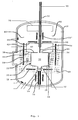
- the inventive device comprises a particularly double-walled housing 10, in which the formed of pressed graphite crucible 20 is arranged.
- the crucible 20 has an inner space 30 (melting or crystallization space) which is formed by walls 22, a cone-shaped bottom 24 in the form of a blunt cone and an upper crucible opening 26 which is partially closed by means of a cover 28.
- a funnel-shaped buffer space 40 is arranged, which is formed from the same material as the crucible 20 and connected to this preferably in one piece.
- the buffer space 40 itself also has side walls 42, a cover 48 and a bottom 44, which is connected to the side walls 22 of the melting vessel 20.
- a cover heater 50, 50 ' is arranged, which is opposite to a bottom heater 52.
- the floor heating 52 is arranged laterally of the germ pocket 32 and kept apart from this, so that the seed crystal present therein does not prematurely melt.
- a water-cooled graphite rod 70 At the bottom of the seed bag contains a water-cooled graphite rod 70. Side of the germ pocket and the water-cooled graphite rod 70 side heating elements 56 are arranged for targeted melting of the seed crystal.
- a temperature measuring element 60 designed as a sliding element is arranged laterally of the crucible 20, with which the exact axial temperature profile can be determined.
- the side walls 22 of the vessel 20 are completely surrounded by an insulating jacket 82.
- the insulating jacket 82 spaces a lateral jacket-shaped support heater 54.
- the heating elements 50, 50 ', 52, 54 and 56 and the crucible 20 with germ pocket 32 and the overlying buffer member 40 are surrounded by an insulating material 80 formed of graphite, which prevents lateral heat flow and only one formed between the cover heating and crucible bottom 24 and bottom heating 52 axial temperature gradient allowed.
- the inventive device has an opening, not shown, for purging with an inert gas or for applying a vacuum.
- a phase sensor 90 extending from the outside through the housing is provided, which contains a displaceable rod 94 located in an outer tube 92, which can be lowered slowly downwards and with which the solid phase interface can be felt.
- the tube 92 may also be connected to the rod 94.
- a capacitor 95 is arranged above the crucible.
- the interior space 30 of the melting vessel 20 is filled with a calcium fluoride mixture which contains additional scavenger materials having a high affinity for oxygen, such as PbF 2 , SnF 2 or CdF 2 , by means of a device not shown in FIG Cover closed and rinsed with nitrogen as inert gas to remove unwanted atmospheric oxygen. Thereafter, a vacuum of 10 -4 mbar (10 -2 Pa) is applied and the cover heater 50, 50 ', the bottom heater 52 and optionally the jacket heater 54 employed and cooled slowly over several hours to 1450 ° C while cooling the germ pocket. The mixture is then homogenized for five days at this temperature, whereby convection is maintained in the melt.
- additional scavenger materials having a high affinity for oxygen such as PbF 2 , SnF 2 or CdF 2
- the bottom heating is driven down to a temperature of 1200 ° C and carefully melted by the seed pocket heater 26 of the seed crystal.
- the lid heater 50, 50 ' is kept constant and the bottom heating is slowly driven down to a temperature below the crystallization point for several days, wherein starting from the seed a monocrystal grows in the direction of the surface of the melt.
- the resulting single crystal has the same orientation as the crystal nucleus.
- the resulting single crystal is annealed and cooled to room temperature over a period of three weeks. In this way, a single crystal having a diameter of 385 cm and a height of 161 mm (without a seed pocket) is obtained.
- the single crystal has a fluctuation of the refractive index ⁇ n of ⁇ 1 ⁇ 10 -6 over the entire crystal volume. Its stress birefringence SDB is ⁇ 1 nm / cm. In addition, the crystal thus obtained exhibits an extremely high radiation resistance.
Landscapes
- Chemical & Material Sciences (AREA)
- Engineering & Computer Science (AREA)
- Crystallography & Structural Chemistry (AREA)
- Materials Engineering (AREA)
- Metallurgy (AREA)
- Organic Chemistry (AREA)
- Inorganic Chemistry (AREA)
- Crystals, And After-Treatments Of Crystals (AREA)
- Liquid Deposition Of Substances Of Which Semiconductor Devices Are Composed (AREA)
- Fodder In General (AREA)
Applications Claiming Priority (2)
| Application Number | Priority Date | Filing Date | Title |
|---|---|---|---|
| DE10010484A DE10010484A1 (de) | 2000-03-03 | 2000-03-03 | Verfahren und Vorrichtung zur Züchtung von großvolumigen orientierten Einkristallen |
| EP01921157A EP1259663B1 (fr) | 2000-03-03 | 2001-03-02 | Procede et dispositif de culture de monocristaux orientes de gros volume |
Related Parent Applications (2)
| Application Number | Title | Priority Date | Filing Date |
|---|---|---|---|
| EP01921157A Division EP1259663B1 (fr) | 2000-03-03 | 2001-03-02 | Procede et dispositif de culture de monocristaux orientes de gros volume |
| EP01921157.2 Division | 2001-03-02 |
Publications (2)
| Publication Number | Publication Date |
|---|---|
| EP1754809A2 true EP1754809A2 (fr) | 2007-02-21 |
| EP1754809A3 EP1754809A3 (fr) | 2010-03-17 |
Family
ID=7633434
Family Applications (2)
| Application Number | Title | Priority Date | Filing Date |
|---|---|---|---|
| EP01921157A Expired - Lifetime EP1259663B1 (fr) | 2000-03-03 | 2001-03-02 | Procede et dispositif de culture de monocristaux orientes de gros volume |
| EP06023376A Withdrawn EP1754809A3 (fr) | 2000-03-03 | 2001-03-02 | Monocristaux volumineux et orientés présentant un indice de réfraction homogène et une faible biréfringence par compression |
Family Applications Before (1)
| Application Number | Title | Priority Date | Filing Date |
|---|---|---|---|
| EP01921157A Expired - Lifetime EP1259663B1 (fr) | 2000-03-03 | 2001-03-02 | Procede et dispositif de culture de monocristaux orientes de gros volume |
Country Status (7)
| Country | Link |
|---|---|
| US (1) | US6969502B2 (fr) |
| EP (2) | EP1259663B1 (fr) |
| JP (1) | JP4195222B2 (fr) |
| AT (1) | ATE447053T1 (fr) |
| AU (1) | AU2001248256A1 (fr) |
| DE (2) | DE10010484A1 (fr) |
| WO (1) | WO2001064975A2 (fr) |
Cited By (1)
| Publication number | Priority date | Publication date | Assignee | Title |
|---|---|---|---|---|
| FR2951739A1 (fr) * | 2009-11-30 | 2011-04-29 | Commissariat Energie Atomique | Dispositif de controle de l'etat d'avancement de la cristallisation d'un bain de materiau fondu dans un procede de solidification dirigee utilisant les ultrasons |
Families Citing this family (29)
| Publication number | Priority date | Publication date | Assignee | Title |
|---|---|---|---|---|
| JP4017863B2 (ja) * | 2001-12-18 | 2007-12-05 | 信越石英株式会社 | アニール炉及び光学用合成石英ガラスの製造方法 |
| RU2002115062A (ru) * | 2002-05-31 | 2004-02-20 | Корнинг Инкорпорейтид (Us) | Способ выращивания монокристаллов фторида кальция |
| US20040099205A1 (en) * | 2002-09-03 | 2004-05-27 | Qiao Li | Method of growing oriented calcium fluoride single crystals |
| US7033433B2 (en) * | 2003-01-24 | 2006-04-25 | Corning Incorporated | Crystal growth methods |
| EP1475464A1 (fr) * | 2003-05-06 | 2004-11-10 | Corning Incorporated | Procédé pour la production d'un cristal optique |
| EP1643017A4 (fr) * | 2003-07-03 | 2009-05-06 | Hitachi Chemical Co Ltd | Creuset et procede de croissance d'un monocristal a l'aide de ce creuset |
| DE10347430B4 (de) * | 2003-10-13 | 2006-04-27 | Schott Ag | Ofen zur Züchtung von Einkristallen aus geschmolzener Kristallrohmasse |
| DE102004003829A1 (de) | 2004-01-26 | 2005-08-18 | Schott Ag | Verfahren zum Reinigen von Kristallmaterial und zum Herstellen von Kristallen, eine Vorrichtung hierzu sowie die Verwendung der so erhaltenen Kristalle |
| DE102004008753A1 (de) | 2004-02-23 | 2005-09-08 | Schott Ag | Herstellung von spannungsarmen, großvolumigen Kristallen mit geringer Spannungsdoppelbrechung und homogener Brechzahl, sowie deren Verwendung |
| DE102004008749A1 (de) * | 2004-02-23 | 2005-09-08 | Schott Ag | Verfahren zur Herstellung eines großvolumigen CaF2-Einkristalles mit geringer Streuung und verbesserter Laserstabilität, sowie ein solcher Kristall und dessen Verwendung |
| DE102004008754A1 (de) * | 2004-02-23 | 2005-09-08 | Schott Ag | Herstellung von spannungsarmen, nicht (111)-orientierten, großvolumigen Einkristallen mit geringer Spannungsdoppelbrechung und homogener Brechzahl, sowie deren Verwendung |
| ATE511089T1 (de) * | 2004-02-23 | 2011-06-15 | Hellma Materials Gmbh & Co Kg | Verfahren zur herstellung von caf2- linsenrohlingen, insbesodere für die 193-nm- und 157-nm-lithographie mit minimierten defekten |
| DE102004008752A1 (de) * | 2004-02-23 | 2005-09-08 | Schott Ag | Herstellung von großvolumigen CaF2-Einkristallen für die Verwendung als optische Bauelemente mit einer optischen Achse parallel zur (100) oder (110)-Kristallachse |
| US20060201412A1 (en) * | 2005-03-08 | 2006-09-14 | Christian Poetisch | Method of making highly uniform low-stress single crystals with reduced scattering |
| DE102005059531A1 (de) | 2005-12-13 | 2007-06-14 | Schott Ag | Herstellung hochreiner, besonders strahlungsbeständiger großvolumiger Einkristalle aus Kristallscherben |
| DE102006017621B4 (de) * | 2006-04-12 | 2008-12-24 | Schott Ag | Vorrichtung und Verfahren zur Herstellung von multikristallinem Silizium |
| JP4388538B2 (ja) * | 2006-09-21 | 2009-12-24 | 新日本製鐵株式会社 | 炭化珪素単結晶製造装置 |
| DE102008033548A1 (de) | 2008-07-17 | 2010-01-21 | Schott Ag | Verfahren zur Optimierung der Zerteilung eines kristallinen Körpers |
| DE102009015113A1 (de) | 2009-03-31 | 2010-10-14 | Schott Ag | Vorrichtung und Verfahren zur Züchtung von Kristallen |
| KR101136143B1 (ko) * | 2009-09-05 | 2012-04-17 | 주식회사 크리스텍 | 사파이어 단결정 성장방법과 그 장치 |
| WO2013019399A2 (fr) * | 2011-08-04 | 2013-02-07 | Gtat Corporation | Procédé de fabrication d'un produit monocristallin |
| CN103160934B (zh) * | 2011-12-18 | 2016-05-18 | 洛阳金诺机械工程有限公司 | 一种生长晶体材料时的温度梯度控制装置及其方法 |
| CN102660767B (zh) * | 2012-05-28 | 2015-06-10 | 哈尔滨工业大学 | 用于电磁冷坩埚定向凝固设备中的冷却过渡接头 |
| CN102766901B (zh) * | 2012-08-20 | 2015-09-30 | 元亮科技有限公司 | 实时可调温度梯度法生长大尺寸高温晶体的装置及方法 |
| CN103409790B (zh) * | 2013-08-01 | 2016-02-03 | 安徽大晟新能源设备科技有限公司 | 准单晶铸锭炉的下加热器升降机构 |
| US20170239386A1 (en) | 2014-08-18 | 2017-08-24 | University Of Cincinnati | Magnesium single crystal for biomedical applications and methods of making same |
| CN108821340B (zh) * | 2018-09-17 | 2024-05-14 | 大冶市都鑫摩擦粉体有限公司 | 一种硫化锑提纯装置 |
| DE102020111456B4 (de) * | 2020-04-27 | 2023-11-16 | Ebner Industrieofenbau Gmbh | Vorrichtung und Verfahren zum Erwärmen mehrerer Tiegel |
| CN115233214A (zh) * | 2022-07-25 | 2022-10-25 | 江苏大学 | 一种振动辅助全域瞬态加热轴类零件熔覆装置及方法 |
Citations (5)
| Publication number | Priority date | Publication date | Assignee | Title |
|---|---|---|---|---|
| JPS6470880A (en) | 1987-09-10 | 1989-03-16 | Minolta Camera Kk | Digital image processor |
| EP0338411A2 (fr) | 1988-04-18 | 1989-10-25 | Solon Technologies, Inc. | Appareil et méthode pour la croissance de grands monocristaux en forme de plaque/plaque épaisse |
| EP0875778A1 (fr) | 1997-03-18 | 1998-11-04 | Nikon Corporation | Système optique de focalisation d'image pour laser ultraviolet |
| JPH11240787A (ja) | 1998-02-27 | 1999-09-07 | Nikon Corp | 蛍石の製造方法及び光リソグラフィー用の蛍石 |
| EP0972863A1 (fr) | 1998-07-16 | 2000-01-19 | Nikon Corporation | Méthode pour le traitement thermique d'un monocristal d'un fluorure et méthode pour sa préparation |
Family Cites Families (11)
| Publication number | Priority date | Publication date | Assignee | Title |
|---|---|---|---|---|
| US4086424A (en) * | 1977-03-31 | 1978-04-25 | Mellen Sr Robert H | Dynamic gradient furnace and method |
| US4286424A (en) * | 1980-04-11 | 1981-09-01 | Deere & Company | Blockage detector for a cotton harvester |
| DE3323896A1 (de) * | 1983-07-02 | 1985-01-17 | Leybold-Heraeus GmbH, 5000 Köln | Verfahren und vorrichtung zum gerichteten erstarren von schmelzen |
| US5372088A (en) * | 1991-12-30 | 1994-12-13 | At&T Bell Laboratories | Crystal growth method and apparatus |
| JPH10101484A (ja) * | 1996-09-30 | 1998-04-21 | Canon Inc | 結晶製造装置及び方法 |
| JP3988217B2 (ja) * | 1997-09-09 | 2007-10-10 | 株式会社ニコン | 大口径蛍石の製造装置および製造方法 |
| JP4154744B2 (ja) | 1997-12-01 | 2008-09-24 | 株式会社ニコン | フッ化カルシウム結晶の製造方法および原料の処理方法 |
| DE69910863T2 (de) | 1998-02-26 | 2004-07-15 | Nikon Corp. | Verfahren zur Herstellung von Calciumfluorid und Calciumfluorid für Fotolithographie |
| DE19912484A1 (de) * | 1999-03-19 | 2000-09-28 | Freiberger Compound Mat Gmbh | Vorrichtung zur Herstellung von Einkristallen |
| US6580098B1 (en) | 1999-07-27 | 2003-06-17 | Toyoda Gosei Co., Ltd. | Method for manufacturing gallium nitride compound semiconductor |
| US6806069B2 (en) * | 2001-01-09 | 2004-10-19 | Pharmachem Laboratories, Inc. | Ubiquinone composition and methods related thereto |
-
2000
- 2000-03-03 DE DE10010484A patent/DE10010484A1/de not_active Withdrawn
-
2001
- 2001-03-02 EP EP01921157A patent/EP1259663B1/fr not_active Expired - Lifetime
- 2001-03-02 WO PCT/DE2001/000790 patent/WO2001064975A2/fr not_active Ceased
- 2001-03-02 US US10/220,115 patent/US6969502B2/en not_active Expired - Fee Related
- 2001-03-02 AU AU2001248256A patent/AU2001248256A1/en not_active Abandoned
- 2001-03-02 AT AT01921157T patent/ATE447053T1/de not_active IP Right Cessation
- 2001-03-02 DE DE50115195T patent/DE50115195D1/de not_active Expired - Lifetime
- 2001-03-02 EP EP06023376A patent/EP1754809A3/fr not_active Withdrawn
- 2001-03-02 JP JP2001563657A patent/JP4195222B2/ja not_active Expired - Fee Related
Patent Citations (5)
| Publication number | Priority date | Publication date | Assignee | Title |
|---|---|---|---|---|
| JPS6470880A (en) | 1987-09-10 | 1989-03-16 | Minolta Camera Kk | Digital image processor |
| EP0338411A2 (fr) | 1988-04-18 | 1989-10-25 | Solon Technologies, Inc. | Appareil et méthode pour la croissance de grands monocristaux en forme de plaque/plaque épaisse |
| EP0875778A1 (fr) | 1997-03-18 | 1998-11-04 | Nikon Corporation | Système optique de focalisation d'image pour laser ultraviolet |
| JPH11240787A (ja) | 1998-02-27 | 1999-09-07 | Nikon Corp | 蛍石の製造方法及び光リソグラフィー用の蛍石 |
| EP0972863A1 (fr) | 1998-07-16 | 2000-01-19 | Nikon Corporation | Méthode pour le traitement thermique d'un monocristal d'un fluorure et méthode pour sa préparation |
Non-Patent Citations (1)
| Title |
|---|
| SPIE, vol. 3424, pages 0277 - 786 |
Cited By (2)
| Publication number | Priority date | Publication date | Assignee | Title |
|---|---|---|---|---|
| FR2951739A1 (fr) * | 2009-11-30 | 2011-04-29 | Commissariat Energie Atomique | Dispositif de controle de l'etat d'avancement de la cristallisation d'un bain de materiau fondu dans un procede de solidification dirigee utilisant les ultrasons |
| WO2011064391A1 (fr) * | 2009-11-30 | 2011-06-03 | Commissariat à l'énergie atomique et aux énergies alternatives | Dispositif de contrôle de l'état d'avancement de la cristallisation d'un bain de matériau fondu dans un procédé de solidification dirigée utilisant les ultrasons |
Also Published As
| Publication number | Publication date |
|---|---|
| WO2001064975A3 (fr) | 2001-12-06 |
| DE50115195D1 (de) | 2009-12-10 |
| EP1754809A3 (fr) | 2010-03-17 |
| AU2001248256A1 (en) | 2001-09-12 |
| US6969502B2 (en) | 2005-11-29 |
| WO2001064975A2 (fr) | 2001-09-07 |
| US20030089307A1 (en) | 2003-05-15 |
| WO2001064975A8 (fr) | 2002-04-11 |
| JP4195222B2 (ja) | 2008-12-10 |
| EP1259663A2 (fr) | 2002-11-27 |
| JP2003525196A (ja) | 2003-08-26 |
| DE10010484A1 (de) | 2001-09-13 |
| ATE447053T1 (de) | 2009-11-15 |
| EP1259663B1 (fr) | 2009-10-28 |
Similar Documents
| Publication | Publication Date | Title |
|---|---|---|
| EP1259663B1 (fr) | Procede et dispositif de culture de monocristaux orientes de gros volume | |
| DE69604452T2 (de) | Verfahren zur Herstellung polykristalliner Halbleiter | |
| Chani et al. | Growth of Y3Al5O12: Nd fiber crystals by micro-pulling-down technique | |
| DE102017206741B4 (de) | Vorrichtung und Verfahren zur Herstellung eines Galliumoxidkristalls | |
| DE69832846T2 (de) | Verfahren und Vorrichtung zur Herstellung polykristalliner Halbleiter-blöcke | |
| DE69830024T2 (de) | Verfahren zur Herstellung polykristalliner Halbleiter | |
| DE112008003497B4 (de) | Verfahren zum Aufwachsen eines Siliziumcarbideinkristalls | |
| DE2461553A1 (de) | Verfahren zum erzeugen von einkristallen | |
| DE10340589A1 (de) | Verfahren zur Züchtung orientierter Calciumfluorid Einkristalle | |
| Chani et al. | Growth of Tb3Ga5O12 fiber and bulk crystals using micro-pulling-down apparatus | |
| DE10124423A1 (de) | Züchten von orientierten Einkristallen mit wiederverwendbaren Kristallkeimen | |
| DE69724612T2 (de) | Vorrichtung und verfahren zur herstellung von kristallen durch die czochralskimethode und durch diese methode hergestellte kristallen | |
| DE10296668T5 (de) | Verfahren zur Züchtung von Kalziumfluorid-Monokristallen | |
| Chen et al. | Growth of AgGaS2 single crystals by modified furnace | |
| DE102005037393B4 (de) | Verfahren sowie Vorrichtung zur Züchtung von grossvolumigen Einkristallen unter Ausbildung einer konvexen Phasengrenzfläche während des Kristallisationsprozesses | |
| DE20122681U1 (de) | Großvolumige orientierte Einkristalle mit homogener Brechzahl und geringer Spannungsdoppelbrechung | |
| DE3587038T2 (de) | Verfahren zur herstellung von polykristallinem material und vorrichtung dafuer. | |
| DE102004003829A1 (de) | Verfahren zum Reinigen von Kristallmaterial und zum Herstellen von Kristallen, eine Vorrichtung hierzu sowie die Verwendung der so erhaltenen Kristalle | |
| DE102009015113A1 (de) | Vorrichtung und Verfahren zur Züchtung von Kristallen | |
| DE68912686T2 (de) | Verfahren zur Herstellung eines Einkristalls aus einer Halbleiter-Verbindung. | |
| Yoon et al. | Compositional homogeneity of potassium lithium niobate crystals grown by micro pulling down method | |
| DE60205904T2 (de) | Vorrichtung zur herstellung von legierungskristallen | |
| DE10324451A1 (de) | Verfahren zum Züchten optischer Fluorit-Einkristalle | |
| EP1475464A1 (fr) | Procédé pour la production d'un cristal optique | |
| DE102020106291B4 (de) | Heizvorrichtung und Verfahren zur Kristallzüchtung mit beweglicher Impfkristallhalterung |
Legal Events
| Date | Code | Title | Description |
|---|---|---|---|
| PUAI | Public reference made under article 153(3) epc to a published international application that has entered the european phase |
Free format text: ORIGINAL CODE: 0009012 |
|
| 17P | Request for examination filed |
Effective date: 20061206 |
|
| AC | Divisional application: reference to earlier application |
Ref document number: 1259663 Country of ref document: EP Kind code of ref document: P |
|
| AK | Designated contracting states |
Kind code of ref document: A2 Designated state(s): AT BE CH CY DE DK ES FI FR GB GR IE IT LI LU MC NL PT SE TR |
|
| RIN1 | Information on inventor provided before grant (corrected) |
Inventor name: SCHATTER, RICHARD Inventor name: ELZNER, PETER Inventor name: AXMANN, HANS-JOERG Inventor name: REICHHARDT, THORSTEN Inventor name: MOERSEN, EWALD, DR. Inventor name: WEHRHAHN, GUNTHER, DR. |
|
| PUAL | Search report despatched |
Free format text: ORIGINAL CODE: 0009013 |
|
| AK | Designated contracting states |
Kind code of ref document: A3 Designated state(s): AT BE CH CY DE DK ES FI FR GB GR IE IT LI LU MC NL PT SE TR |
|
| RIC1 | Information provided on ipc code assigned before grant |
Ipc: C30B 11/00 20060101AFI20100208BHEP Ipc: C30B 29/12 20060101ALI20100208BHEP Ipc: G02B 5/30 20060101ALI20100208BHEP |
|
| 17Q | First examination report despatched |
Effective date: 20100824 |
|
| RAP1 | Party data changed (applicant data changed or rights of an application transferred) |
Owner name: HELLMA MATERIALS GMBH & CO. KG |
|
| AKX | Designation fees paid |
Designated state(s): AT BE CH CY DE DK ES FI FR GB GR IE IT LI LU MC NL PT SE TR |
|
| STAA | Information on the status of an ep patent application or granted ep patent |
Free format text: STATUS: THE APPLICATION IS DEEMED TO BE WITHDRAWN |
|
| 18D | Application deemed to be withdrawn |
Effective date: 20111004 |