EP1755073A2 - RFID inlay et méthodes de fabrication - Google Patents
RFID inlay et méthodes de fabrication Download PDFInfo
- Publication number
- EP1755073A2 EP1755073A2 EP06119025A EP06119025A EP1755073A2 EP 1755073 A2 EP1755073 A2 EP 1755073A2 EP 06119025 A EP06119025 A EP 06119025A EP 06119025 A EP06119025 A EP 06119025A EP 1755073 A2 EP1755073 A2 EP 1755073A2
- Authority
- EP
- European Patent Office
- Prior art keywords
- rfid
- strap
- der
- substrate
- manufacturing
- Prior art date
- Legal status (The legal status is an assumption and is not a legal conclusion. Google has not performed a legal analysis and makes no representation as to the accuracy of the status listed.)
- Withdrawn
Links
Images










Classifications
-
- G—PHYSICS
- G06—COMPUTING OR CALCULATING; COUNTING
- G06K—GRAPHICAL DATA READING; PRESENTATION OF DATA; RECORD CARRIERS; HANDLING RECORD CARRIERS
- G06K19/00—Record carriers for use with machines and with at least a part designed to carry digital markings
- G06K19/06—Record carriers for use with machines and with at least a part designed to carry digital markings characterised by the kind of the digital marking, e.g. shape, nature, code
- G06K19/067—Record carriers with conductive marks, printed circuits or semiconductor circuit elements, e.g. credit or identity cards also with resonating or responding marks without active components
- G06K19/07—Record carriers with conductive marks, printed circuits or semiconductor circuit elements, e.g. credit or identity cards also with resonating or responding marks without active components with integrated circuit chips
- G06K19/077—Constructional details, e.g. mounting of circuits in the carrier
- G06K19/07745—Mounting details of integrated circuit chips
-
- G—PHYSICS
- G06—COMPUTING OR CALCULATING; COUNTING
- G06K—GRAPHICAL DATA READING; PRESENTATION OF DATA; RECORD CARRIERS; HANDLING RECORD CARRIERS
- G06K19/00—Record carriers for use with machines and with at least a part designed to carry digital markings
- G06K19/06—Record carriers for use with machines and with at least a part designed to carry digital markings characterised by the kind of the digital marking, e.g. shape, nature, code
- G06K19/067—Record carriers with conductive marks, printed circuits or semiconductor circuit elements, e.g. credit or identity cards also with resonating or responding marks without active components
- G06K19/07—Record carriers with conductive marks, printed circuits or semiconductor circuit elements, e.g. credit or identity cards also with resonating or responding marks without active components with integrated circuit chips
- G06K19/077—Constructional details, e.g. mounting of circuits in the carrier
- G06K19/07718—Constructional details, e.g. mounting of circuits in the carrier the record carrier being manufactured in a continuous process, e.g. using endless rolls
-
- G—PHYSICS
- G06—COMPUTING OR CALCULATING; COUNTING
- G06K—GRAPHICAL DATA READING; PRESENTATION OF DATA; RECORD CARRIERS; HANDLING RECORD CARRIERS
- G06K19/00—Record carriers for use with machines and with at least a part designed to carry digital markings
- G06K19/06—Record carriers for use with machines and with at least a part designed to carry digital markings characterised by the kind of the digital marking, e.g. shape, nature, code
- G06K19/067—Record carriers with conductive marks, printed circuits or semiconductor circuit elements, e.g. credit or identity cards also with resonating or responding marks without active components
- G06K19/07—Record carriers with conductive marks, printed circuits or semiconductor circuit elements, e.g. credit or identity cards also with resonating or responding marks without active components with integrated circuit chips
- G06K19/077—Constructional details, e.g. mounting of circuits in the carrier
- G06K19/07749—Constructional details, e.g. mounting of circuits in the carrier the record carrier being capable of non-contact communication, e.g. constructional details of the antenna of a non-contact smart card
-
- G—PHYSICS
- G06—COMPUTING OR CALCULATING; COUNTING
- G06K—GRAPHICAL DATA READING; PRESENTATION OF DATA; RECORD CARRIERS; HANDLING RECORD CARRIERS
- G06K19/00—Record carriers for use with machines and with at least a part designed to carry digital markings
- G06K19/06—Record carriers for use with machines and with at least a part designed to carry digital markings characterised by the kind of the digital marking, e.g. shape, nature, code
- G06K19/067—Record carriers with conductive marks, printed circuits or semiconductor circuit elements, e.g. credit or identity cards also with resonating or responding marks without active components
- G06K19/07—Record carriers with conductive marks, printed circuits or semiconductor circuit elements, e.g. credit or identity cards also with resonating or responding marks without active components with integrated circuit chips
- G06K19/077—Constructional details, e.g. mounting of circuits in the carrier
- G06K19/07749—Constructional details, e.g. mounting of circuits in the carrier the record carrier being capable of non-contact communication, e.g. constructional details of the antenna of a non-contact smart card
- G06K19/0775—Constructional details, e.g. mounting of circuits in the carrier the record carrier being capable of non-contact communication, e.g. constructional details of the antenna of a non-contact smart card arrangements for connecting the integrated circuit to the antenna
- G06K19/07752—Constructional details, e.g. mounting of circuits in the carrier the record carrier being capable of non-contact communication, e.g. constructional details of the antenna of a non-contact smart card arrangements for connecting the integrated circuit to the antenna using an interposer
-
- H—ELECTRICITY
- H05—ELECTRIC TECHNIQUES NOT OTHERWISE PROVIDED FOR
- H05K—PRINTED CIRCUITS; CASINGS OR CONSTRUCTIONAL DETAILS OF ELECTRIC APPARATUS; MANUFACTURE OF ASSEMBLAGES OF ELECTRICAL COMPONENTS
- H05K3/00—Apparatus or processes for manufacturing printed circuits
- H05K3/30—Assembling printed circuits with electric components, e.g. with resistors
- H05K3/32—Assembling printed circuits with electric components, e.g. with resistors electrically connecting electric components or wires to printed circuits
-
- H—ELECTRICITY
- H10—SEMICONDUCTOR DEVICES; ELECTRIC SOLID-STATE DEVICES NOT OTHERWISE PROVIDED FOR
- H10W—GENERIC PACKAGES, INTERCONNECTIONS, CONNECTORS OR OTHER CONSTRUCTIONAL DETAILS OF DEVICES COVERED BY CLASS H10
- H10W90/00—Package configurations
-
- H—ELECTRICITY
- H05—ELECTRIC TECHNIQUES NOT OTHERWISE PROVIDED FOR
- H05K—PRINTED CIRCUITS; CASINGS OR CONSTRUCTIONAL DETAILS OF ELECTRIC APPARATUS; MANUFACTURE OF ASSEMBLAGES OF ELECTRICAL COMPONENTS
- H05K2201/00—Indexing scheme relating to printed circuits covered by H05K1/00
- H05K2201/03—Conductive materials
- H05K2201/0332—Structure of the conductor
- H05K2201/0335—Layered conductors or foils
- H05K2201/0347—Overplating, e.g. for reinforcing conductors or bumps; Plating over filled vias
-
- H—ELECTRICITY
- H05—ELECTRIC TECHNIQUES NOT OTHERWISE PROVIDED FOR
- H05K—PRINTED CIRCUITS; CASINGS OR CONSTRUCTIONAL DETAILS OF ELECTRIC APPARATUS; MANUFACTURE OF ASSEMBLAGES OF ELECTRICAL COMPONENTS
- H05K2201/00—Indexing scheme relating to printed circuits covered by H05K1/00
- H05K2201/10—Details of components or other objects attached to or integrated in a printed circuit board
- H05K2201/10613—Details of electrical connections of non-printed components, e.g. special leads
- H05K2201/10621—Components characterised by their electrical contacts
- H05K2201/10727—Leadless chip carrier [LCC], e.g. chip-modules for cards
-
- H—ELECTRICITY
- H05—ELECTRIC TECHNIQUES NOT OTHERWISE PROVIDED FOR
- H05K—PRINTED CIRCUITS; CASINGS OR CONSTRUCTIONAL DETAILS OF ELECTRIC APPARATUS; MANUFACTURE OF ASSEMBLAGES OF ELECTRICAL COMPONENTS
- H05K2203/00—Indexing scheme relating to apparatus or processes for manufacturing printed circuits covered by H05K3/00
- H05K2203/07—Treatments involving liquids, e.g. plating, rinsing
- H05K2203/0703—Plating
- H05K2203/0723—Electroplating, e.g. finish plating
-
- H—ELECTRICITY
- H05—ELECTRIC TECHNIQUES NOT OTHERWISE PROVIDED FOR
- H05K—PRINTED CIRCUITS; CASINGS OR CONSTRUCTIONAL DETAILS OF ELECTRIC APPARATUS; MANUFACTURE OF ASSEMBLAGES OF ELECTRICAL COMPONENTS
- H05K2203/00—Indexing scheme relating to apparatus or processes for manufacturing printed circuits covered by H05K3/00
- H05K2203/15—Position of the PCB during processing
- H05K2203/1545—Continuous processing, i.e. involving rolls moving a band-like or solid carrier along a continuous production path
-
- H—ELECTRICITY
- H05—ELECTRIC TECHNIQUES NOT OTHERWISE PROVIDED FOR
- H05K—PRINTED CIRCUITS; CASINGS OR CONSTRUCTIONAL DETAILS OF ELECTRIC APPARATUS; MANUFACTURE OF ASSEMBLAGES OF ELECTRICAL COMPONENTS
- H05K3/00—Apparatus or processes for manufacturing printed circuits
- H05K3/22—Secondary treatment of printed circuits
- H05K3/24—Reinforcing of the conductive pattern
- H05K3/241—Reinforcing of the conductive pattern characterised by the electroplating method; means therefor, e.g. baths or apparatus
- H05K3/242—Reinforcing of the conductive pattern characterised by the electroplating method; means therefor, e.g. baths or apparatus characterised by using temporary conductors on the printed circuit for electrically connecting areas which are to be electroplated
-
- H—ELECTRICITY
- H05—ELECTRIC TECHNIQUES NOT OTHERWISE PROVIDED FOR
- H05K—PRINTED CIRCUITS; CASINGS OR CONSTRUCTIONAL DETAILS OF ELECTRIC APPARATUS; MANUFACTURE OF ASSEMBLAGES OF ELECTRICAL COMPONENTS
- H05K3/00—Apparatus or processes for manufacturing printed circuits
- H05K3/22—Secondary treatment of printed circuits
- H05K3/24—Reinforcing of the conductive pattern
- H05K3/245—Reinforcing conductive patterns made by printing techniques or by other techniques for applying conductive pastes, inks or powders; Reinforcing other conductive patterns by such techniques
- H05K3/246—Reinforcing conductive paste, ink or powder patterns by other methods, e.g. by plating
-
- H—ELECTRICITY
- H10—SEMICONDUCTOR DEVICES; ELECTRIC SOLID-STATE DEVICES NOT OTHERWISE PROVIDED FOR
- H10W—GENERIC PACKAGES, INTERCONNECTIONS, CONNECTORS OR OTHER CONSTRUCTIONAL DETAILS OF DEVICES COVERED BY CLASS H10
- H10W72/00—Interconnections or connectors in packages
- H10W72/01—Manufacture or treatment
- H10W72/0198—Manufacture or treatment batch processes
Definitions
- the present invention relates to radio frequency identification (RFID). More particularly, the present invention relates to RFID inlays and methods of their manufacture. BACKGROUND OF THE INVENTION
- Radio frequency identification is a technology having many applications including, for example, inventory control, supply chain management, and anti-theft of merchandise in stores.
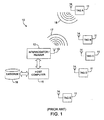
- a typical RFID system 10 comprises a plurality of transponders (or “tags”) 11 and one or more transceivers (referred to in the art as “interrogators” or “readers”) 12, as illustrated in FIG. 1.
- the tags 11 are attached to objects, such as for example, products in a supermarket.
- An interrogator/reader 12 includes an antenna 13.
- the tags 11 also have their own respective antennas 14.
- the interrogator/reader 12 "interrogates" a particular tag 11 by transmitting a radio frequency interrogation signal 17 to the tag (e.g. TAG A in FIG. 1).
- the interrogation signal 17 activates the interrogated tag, which then transmits or reflects a radio frequency signal 18 carrying a unique identifier or other related information back to the interrogator/reader 12.
- the interrogator/reader 12 "reads" the information by demodulating the radio frequency signal 18. The information is then either communicated directly to a host computer 15 and stored in a database 16, or is stored locally in the interrogator/reader 12 and later uploaded to the host computer 15 for processing.
- An RFID tag comprises: (1) an RFID integrated circuit (or "chip"), which contains circuitry and memory for storing the unique identifiers and possibly other information; (2) a substrate upon which the RFID chip is mounted; and (3) an antenna that is properly tuned for communication with the interrogator/reader. While substantial strides have been made in reducing the costs involved in fabricating the RFID chips, inexpensive methods of assembling the RFID chips with the remaining components that make up the tag have lagged. In other words, expensive assembly and manufacturing costs remain as bottlenecks to achieving the economies of scale necessary to render RFID economically feasible. Various of the assembly and manufacturing challenges faced by RFID tag manufactures, and some of the attempts to overcome the challenges are described below.
- RFID chips are manufactured using integrated circuit technology.
- the size of a resulting RFID chip may be as small as the size of a grain of salt.
- the required length of a typical RFID tag antenna may be on the order of 100 mm. This length of antenna is necessary for the antenna to be able to transmit and receive radio frequency signals of the wavelength used in RFID systems. Consequently, in nearly all applications, the antenna dimensions prohibit integration of the antenna in the RFID chip fabrication process.
- the antenna must therefore be manufactured separately, i.e. on a separate substrate, and then somehow assembled with and electrically connected to the RFID chip.
- One known method of assembling an RFID chip to its respective antenna employs a robot to precisely position contacts of the RFID chip to contact positions of the RFID tag antenna formed on an antenna substrate. Once properly positioned, a bonding process is performed to form a permanent electrical connection between the chip contacts and the antenna. Because the dimensions of the RFID chip and its contacts are extremely small compared to the dimensions of the antenna, the process of properly aligning the chip contacts to the antenna contact positions is slow and tedious. Further, because the chips are so small, even very sophisticated robots have difficulty picking up and handling the chips.
- a strap 20 comprises an RFID chip 22, a substrate 21 that functions as a carrier of the RFID chip, and electrically conductive pads 24 formed on the strap substrate surface.
- the pads 24 on the strap substrate 21 are used to electrically connect the chip contacts to the antenna contact positions 26 on an antenna substrate 27. Because the strap pads 24 are much larger and spaced a greater distance apart than the chip contacts are, forming an electrical connection between the chip contacts and the antenna 28 is substantially less difficult than forming the connections without the benefit of the strap 20.
- a plurality of strap substrates may be formed in a single operation by embossing a long strip or web of substrate material using an embossing tool. Such an approach is shown in FIG. 3.
- a plurality of recessed regions 30 is formed by rolling an embossing tool 32 over a rigid or semi-rigid substrate 34 and applying pressure and/or heat.
- the recessed regions 30 are of a predetermined size approximating the dimensions of the chip.
- a drawback of the embossing tool is that sophisticated equipment and machinery are needed to apply and control the applied pressure and/or heat.
- the substrate material is heated and cooled under pressure for efficient embossing.
- the equipment is necessarily large and lacks flexibility.
- embossing approach Another drawback of the embossing approach is that, unless the thickness, Y, of the substrate material is large enough, embossing the topside of the substrate 34 results in protrusions 36 extending out from the backside surface of the substrate 34 and/or strained areas around the embossed features, and the strained areas result in high yield loss.
- the protrusions 36 also make it difficult to assemble the strap to the antenna substrate.
- the protrusions 36 can be avoided by using a more rigid substrate material or by increasing the thickness Y. However, increased rigidity makes embossing more difficult. Increased rigidity or thickness Y of the substrate also prevents the substrate from being rolled onto a reel. In some applications, it is desirable to form straps on a flexible substrate that can be rolled onto a reel. This allows for easier handling and delivery to customers.
- the RFID chips are placed in the recessed regions 30 by hand or by a robot (similar to as described above).
- the RFID chips are assembled into the recessed regions using a process known as fluidic self-assembly (FSA).
- FSA fluidic self-assembly
- FIG. 4 the FSA process involves flowing a slurry 40 containing numerous RFID chips 42 over the surface of the strap substrate 34 having the recessed regions 30. Gravity pulls the RFID chips into the recessed regions 30.
- edges 44 of the RFID chips 42 may beveled so that they more easily fall into the recessed regions 30 with the correct orientation.
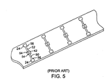
- first and second leads 50 and 52 are formed for each RFID chip 42.
- the first and second leads 50, 52 both have proximate ends 54 that electrically connect to the RFID chip contacts (not shown) and distal ends 56.
- the first and second leads 50, 52 are formed so that they extend in opposite directions away from the RFID chip 42 and toward the longitudinal edges of the substrate, where they terminate in the form of pads (i.e. pads 24).
- the leads and pads are formed by a photoresist, cure, and etching process, similar to that used in the manufacture of integrated circuits.
- the photoresist, cure, and etching process requires multiple steps and is slow.
- Such a process is also environmentally unfriendly, since it uses harmful chemicals and generates byproducts that are both harmful to the manufacturer and to the environment.
- the process is expensive.
- a second prior art technique for forming the interconnecting leads and pads is described in U.S. Patent No. 6,867,983 ('983 Patent).
- a catalyst layer is selectively formed on the substrate where the leads and pads are to be located.
- a metal such as copper, is plated on the activated layers using an electroless plating process.
- the '983 patent explains that the catalyst layer is made up of elements from Group 1B or VIII of the periodic table.
- a variety of suitable materials that can be used for the catalyst layer include PVC powder, palladium dichloride bisacetonitrile (PdC12BAN), lithium chloride (LiCl) in tetrahydorfuran (THF) solution, PdCl 2 , and Pd(NO 3 ) 2 .
- Electroless plating techniques also require extensive process lines requiring high water consumption, are waste intensive, and generate large amounts of toxic waste.
- Electroless plating cannot be used to reliably form electrical interconnects between the conductive pads on the strap and the antenna contacts on the antenna substrate because it has poor bridging capabilities.
- FIG. 6 shows a prior art RFID inlay 60 in which a conductive epoxy is used to form electrical interconnections between the electroless plated strap pads and antenna contacts.
- the RFID inlay 60 includes an antenna substrate 61 having antenna contacts 62.
- a strap substrate 63 is physically mounted and secured to the antenna substrate 61 by an adhesive 64.
- the strap substrate 63 includes electroless plated strap pads 65, and a recessed region 66 within which an RFID chip 67 is held.
- the electroless plated strap pads 65 are electrically connected to chip contacts 68 of the RFID chip 67.
- a conductive epoxy 69 is formed between the electroless plated strap pads 65 on the strap substrate 63 and the antenna contacts 62 on the antenna substrate 61.
- conductive epoxies may be used to form the electrical interconnects between the strap pads and the antenna contacts, multiple processing steps are still needed to complete the electrical interconnections and the mechanical assembly of the RFID inlay. Further, because the conductive adhesives must cure over a period of time (typically minutes or even hours), completed RFID inlays cannot be tested immediately following assembly. With production rates measured in thousands of units per hour, this means that any delay in testing can result in substantial yield losses before a defect in the manufacturing process is detected.
- An exemplary RFID inlay structure comprises an inlay substrate having an antenna and antenna contacts; a strap substrate carrying an RFID chip and having at least one surface coated with a directly electroplateable resin (DER) or other electrically conductive material; and an electroplated metal interconnection layer interconnecting contacts of the RFID chip to the antenna contacts on the inlay substrate.
- DER directly electroplateable resin
- a method of manufacturing an RFID inlay structure includes providing a strap substrate having a recessed region for accommodating an RFID chip. Strap pad patterns, adjacent to the recessed regions, are formed from known prior art techniques or using a directly electroplateable resin (DER). The strap substrate is then attached to an inlay substrate having an electrically conductive antenna and antenna contact patterns. The strap pad patterns, antenna pattern and antenna contacts, any of which may be formed using DER, are electroplated. In this manner a seamless metal interconnect is formed between contacts of the RFID chip and the antenna contacts on the inlay substrate, thereby eliminating the need to deposit conductive epoxies or glues to achieve the electrical interconnection between the chip contacts and the antenna contacts.
- DER directly electroplateable resin
- the strap substrate may be obtained from a web or sheet of strap substrates formed by a casting process.
- the casting process comprises casting a low viscosity material onto a casting drum or conveyor having predetermined casting patterns.
- the substrates are formed by curing the low viscosity material (e.g., using one or more ultraviolet sources, heat or other methods) as the material is conveyed around the casting drum or conveyor.
- RFID chips may then be assembled into the recessed regions of the strap substrate (web or sheet form) using a fluidic self-assembly (FSA), vibration self-assembly, or other suitable technique.
- FSA fluidic self-assembly
- vibration self-assembly or other suitable technique.
- the strap pad patterns (and possibly other features, e.g., loop antenna patterns) are formed on the substrate (web or sheet). Edges of the strap substrate may also be dipped into a DER solution in preparation of an electroplating process. The DER coated edges facilitate the electroplating to form seamless metal coverage of all required electrical paths.
- the web or sheet of strap substrates may then be either plated or separated into long strips, each strip having a succession of strap substrates with corresponding RFID chips in associated recessed regions and corresponding strap pad patterns or loop antenna patterns.
- the DER material is formulated to form a DER ink capable of being applied to the web of strap substrates to form strap pad patterns or loop antenna patterns.
- DER may also be used to form antenna features and antenna contact patterns on the inlay substrate.
- the DER ink may also be formulated so that it can be applied by a pen of a pen-plotter apparatus.
- the DER ink comprises a binder or co-binder and at least one conductive powder having a mean particle size of less than 2 microns or less.
- the conductive powder may contain carbon black and/or graphite. Use of graphite may also operate as a lubricant to provide lubrication for the pen of the pen-plotter apparatus.
- DER antenna loop patterns are formed on the same substrate that the RFID chips are mounted.
- the RFID chips are mounted to the substrate prior to forming the DER antenna loop patterns.
- the antenna loop patterns are formed.
- the DER ink is also applied onto the RFID chip contacts.
- One or more bus bars are also formed on the substrate using the DER ink to facilitate an electroplating process that electroplates the antenna loop patterns and the DER that was applied to the RFID chip contacts.
- FIG. 1 is a conceptual drawing of a conventional RFID system.
- FIG. 2 is a perspective view drawing of a prior art RFID inlay substrate having an antenna and its association with a strap containing an RFID chip.
- FIG. 3 is a drawing illustrating a known embossing technique used to form recessed regions in a strap substrate.
- FIG. 4 is a drawing illustrating a prior art fluidic self-assembly (FSA) technique.
- FIG. 5 is a perspective drawing of a plurality of recesses, for holding a corresponding plurality of RFID chips, and associated leads for electrically interconnecting contacts of the RFID chips to antenna contact positions on an inlay substrate.
- FIG. 6 is a cross-sectional drawing of a prior art RFID inlay that employs a conductive epoxy or conductive glue to form the electrical interconnections between electroless plated strap pads of a strap substrate and antenna contacts of an antenna substrate.
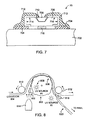
- FIG. 7 is a cross-sectional drawing of an RFID inlay structure, according to an embodiment of the present invention.
- FIG. 8 is a drawing of a casting technique that uses a casting drum, which can be used to form a web containing a plurality of strap substrates, in accordance with the present invention.
- FIG. 9 is a drawing of a casting technique that uses conveyor having a casting belt, which can be used to form a web containing a plurality of strap substrates, in accordance with the present invention.
- FIG. 10 is a perspective view drawing of a web containing a plurality of recessed regions formed, for example, by the casting technique shown in FIG. 8 or the belt-conveyor casting technique shown in FIG. 9.
- FIG. 11 is a flow diagram illustrating the manufacture of a directly electroplateable resin (DER) ink that is suitable for application by a pen plotter apparatus, according with an aspect of the present invention.
- DER directly electroplateable resin
- FIG. 12 is a flow diagram illustrating a method of forming DER patterns on strap and/or inlay substrates using a DER ink printing technique, in accordance with an aspect of the present invention.
- FIG. 13 is a top view drawing of a web of strap substrates following performance of the DER printing method shown in FIG. 12.
- FIG. 14 is a top view drawing of a portion of an inlay substrate roll following performance of the DER printing method shown in FIG. 12.
- FIG. 15 is a flow diagram illustrating a strap preparation process, in accordance with an aspect of the present invention.
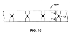
- FIG. 16 is a top view drawing of a strip containing a plurality of straps following the web-cutting step in the strap preparation process shown in FIG. 15.
- FIG. 17 is a perspective view drawing of a strip containing a plurality of straps following a DER edge-dipping step in the strap preparation process shown in FIG. 15.
- FIG. 18 is a top view drawing of a DER edge treated strap following the DER edge dipping and strap cutting steps in the strap preparation process shown in FIG. 15.
- FIG. 19 is a flow diagram illustrating a strap mounting process for assembling the DER edge treated straps in FIG. 18 onto the inlay substrates of the inlay roll in FIG. 14, according to an aspect of the present invention.
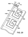
- FIG. 20 is a top perspective view drawing illustrating the mounting of a strap onto an inlay substrate, according to an aspect of the present invention.
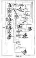
- FIG. 21 is a flow diagram illustrating an electroplating process and various label lamination techniques, in accordance with aspects of the present invention.
- FIG. 22 is a cross-sectional drawing of an exemplary RFID label manufactured in accordance with the methods of the present invention.
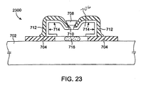
- FIG. 23 is a cross-sectional drawing of an RFID inlay structure, according to an alternative embodiment of the present invention.
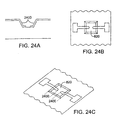
- FIG. 24A-C are cross-sectional, top and perspective view drawings, respectively, of a strap with DER strap pad extension patterns for the RFID inlay structure shown in FIG. 23.
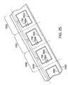
- FIG. 25 shows a perspective drawing of a plurality of RFID inlay structures, according to an embodiment of the present invention.
- FIG. 26 is a drawing of a test/inspection apparatus, according to an embodiment of the present invention.
- FIG. 27 is a top view drawing of an exemplary sheet of RFID inlays containing different RFID tag types that can be tested using the test/inspection apparatus shown in FIG. 26.
- the RFID inlay structure 70 comprises an inlay substrate (i.e. antenna substrate) 702, upon which an antenna having antenna contacts 704 are formed; a strap substrate 706; and an RFID chip 708.
- Conductive bumps (or other chip contacts) 710 of the RFID chip 708 are electrically connected to the antenna contacts 704 by way of an electroplated metal layer 712 formed over a layer of directly electroplateable resin (DER) 714.
- DER directly electroplateable resin
- Edges of the strap substrate 706 may also be coated with a DER layer, which as explained in more detail below helps to ensure that the electroplating layer 712, when formed, forms a continuous electrical connection between the antenna contacts 704 and the chip contacts 710.
- a pressure sensitive adhesive (PSA) 816 or other suitable adhesive may also be applied between the strap substrate 706 and the inlay substrate 702. The PSA 816 prevents movement of the strap during the electroplating process.
- the inlay substrate 702 may be formed from various polymeric materials, e.g., polyethylene, or may be formed from paper, laminations of paper and a polymeric film. Further, the inlay substrate 702 may be rigid or flexible. If flexible, a plurality of antennas formed on a single long roll of substrates may be conveniently wound on a reel.
- the plurality of antennas and corresponding antenna contacts 704 may be formed from a conductive ink, DER (e.g. when the strap pad patterns are patterned using DER), electroplating, deposition or sputtering methods (e.g. vapor deposition), conventional etching techniques, or other suitable method.
- the DER used to print the antennas and corresponding antenna contacts 704 is formulated so that it is compatible with the DER formula used to form the strap pad patterns. This helps to ensure that even plating occurs during the electroplating process.
- the strap substrate 706 may be formed using conventional embossing methods such as, for example, those describe above.
- a plurality of straps may be formed using a casting technique, according to an embodiment of the present invention.
- a low viscosity material e.g. a UV curable acrylate epoxy or low-shrinkage polymer ((UV curable or non-UV curable) that can be cast in liquid form
- the casting drum 802 has a plurality of casting patterns 806 around the drum's circumference, and a first ultraviolet source 808 in its interior.
- Rollers 810 and 812 continuously convey the conveyor belt 804 around the casting drum 802 while the low viscosity material 800 is injected from an injector 814 between the drum surface and the bottom surface of the conveyor belt 804.
- the first ultraviolet source 808 operates to partially cure the low viscosity material 800 as the casting drum 802 turns.
- a separator 816 separates the semi-cured material, as a second ultraviolet source 818 cures the material to its final form.
- an endless belt 902, as shown in FIG. 9, having casting patterns 904 may be employed to forma plurality of straps.
- An advantage of this approach is that the casted patterns are formed on a flat surface, and therefore a better representation of the desired features may be obtained than can be achieved with a casting drum.
- the above casting techniques are suitable for reel-to-reel processing, whereby the finished web may be rolled onto a reel for easy storage and transport to further processing and assembly stations.
- rigid flat sheets of substrates may be preferable.
- a glass plate e.g. 18" x 24
- the low-viscosity material may be cast over it using, for example, a drawdown coater. In this manner, very thin, yet rigid substrates can be created.
- the resulting substrate sheet (or "web") 1000 contains a plurality of recessed regions 820 formed by the casting process.
- the recessed regions 820 are used to accommodate RFID chips 708 placed, for example, using a fluidic or vibration assembly process.
- the cured substrate sheet may be stored in roll form by winding the finished product on a reel.
- different drums having different casting patterns 806 may be employed to cast recessed regions 820 having different dimensions (e.g. to accommodate RFID chips of different sizes; or to vary recess-to-recess spacing).
- the thickness of the substrate sheet can be easily changed and controlled, depending on the application.
- the material is not stressed to create the recessed regions 820, and the recessed regions 820 retain their dimensional characteristics much better than recessed regions formed by embossing methods.
- a first step in the method is that of providing a substrate, web or sheet 1000, for example similar to that shown in FIG. 10, having a plurality of recessed regions 820 sufficient in size to accommodate the RFID chips 708.
- the RFID chips 708 are assembled into the recessed regions 820 of the web using a fluidic self assembly (FSA) process, as described for example in U.S. Patent No. 5,545,291 .
- FSA fluidic self assembly
- the RFID chips 708, which have been preformed with beveled edges (as previously described) are mixed in a fluid (e.g. water, acetone and/or alcohol) to form a slurry.
- the slurry is flowed over the top surface of the web, whereupon the chips fall and self-align into the recessed regions 820.
- Other assembly methods besides FSA may be used.
- vibration self-assembly whereby the RFID chips are vibrated over the web surface until the RFID chips self-align into the recessed regions 820, may also be used.
- directly electroplateable resin (DER) strap pad patterns 714 are formed on the upper surface and, optionally, edges (including a portion of the bottom surface along the edges) of the strap substrate.
- DER directly electroplateable resin
- One or more plating bus bars may also be printed on the strap substrate with DER (similar to that shown in FIG. 14 below for the antenna substrate), depending on the application.
- the bus bars serve as electrical terminals which the electroplating equipment can connect to during the electroplating process.
- the DER material comprises a binder (i.e. resin) or co-binder and at least one conductive powder having a mean particle size of 2 microns or less.
- the conductive powder may contain carbon black and/or graphite in the amount sufficient to produce a "microscopic" electrical volume resistivity of less than 1000 ohm-cm (e.g., less than 100, 10 or 1 ohm-cm).
- a presence of sulfur in amounts greater than about 0.1 % by weight of the overall composition, may be added.
- DER materials are desirable since they do not require any pretreatment prior to being electroplated. They can also be applied very rapidly, and require no electrical bonding operations. These attributes make DER materials well suited for the manufacture of RFID inlays.
- the DER material may be formulated to produce a low viscosity DER solution or DER "ink” (not to be confused with prior art non-DER inks).
- the DER ink may comprise, for example an evaporating solvent and a heat curing catalyst, such that when the solvent evaporates, the DER coating remains uncured and has flow properties that allow setting of the RFID chip. Once heat is applied to the assembly, the polymer hardens and the chip is secured.
- a plotter pen of a conventional plotter apparatus may be used to form the DER patterns. Application by a plotter pen further shortens the time required to form the DER patterns, is more precise than techniques used in the prior art, and, consequently, results in lower manufacturing and assembly costs.
- FIG. 11 is a flow diagram illustrating the manufacture of a DER ink, including that suitable for application by a pen of a conventional pen-plotter apparatus, according to an aspect of the present invention.
- the basic formulation for the DER is that described in U.S. Patent No. 6,582,887 to Luch.
- the binder and carriers solvent (if any) are measured and mixed using known methods. Powders and additives are mixed to the binder/carrier solution following methodology known in the field, to optimize dispersion and particle size distribution forming a slurry. Appropriate amounts of materials such as graphite, aluminum powders, oxides, etc. may also be added to serve as a lubricants or cleaners to aid the performance of the pen.
- the resulting slurry may be milled, if necessary, to further reduce the particle size and/or optimize dispersion necessary for proper performance of the pen of the pen-plotter apparatus.
- One or more of the particle size, wettability, resistivity, and adhesion characteristics after milling are then measured to characterize the ink. Once the ink meets the required specifications, it is collected and stored. Based on the measurements, additional carbon black, sulfur, graphite, and/or solvent are added to the ink (or "slurry"), and further milling is performed if necessary to achieve the desired DER ink characteristics.
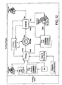
- Figure 12 is a flow diagram illustrating an exemplary method of forming DER patterns using a DER ink printing technique, according to an embodiment of the invention.
- the DER printing technique describe herein may be used to print strap pad patterns 714 or loop antenna patterns on strap substrates 706, and may also be used to print antenna features and antenna contact patterns on the inlay substrate 702.
- a sheet or roll of strap substrate material is first provided.
- the sheet or roll of strap substrate material is preferably in the form of a web of strap substrates having a plurality of casted recessed regions 820 with corresponding RFID chips 708.
- a DER ink supply for example as manufactured in accordance with the DER ink manufacturing process shown in FIG. 11, is configured for application by the printing tool (e.g. pen-plotter apparatus). Process parameters are provided to the printing tool.
- the printing process is performed to form the DER strap pads patterns 714 (on the strap substrate 706).
- the printed strap substrate sheets are stored and subsequently transferred to an evaluation station, where each of the strap substrates 706 of the strap substrate sheet is evaluated to determine whether the intended characteristics (pattern dimensions, thickness, electrical characteristics, etc.) have been achieved.
- FIG. 13 shows a top view of a web of strap substrates (outlined by dashed lines) following the printing process of FIG. 12. As shown, each of the recessed regions contains an RFID chip 708. DER strap pad patterns 714 have been printed over a portion of the strap substrates as shown, and in contact with the chip contacts of each of the RFID chips 708. The DER strap pad patterns 714 are used later in the RFID inlay manufacturing process to electroplate an electrically conductive interconnect between the chip contacts of the RFID chips 708 and the antenna contacts formed on the inlay substrate.
- the DER printing technique in FIG. 12 may also be employed to print DER antenna features, antenna contact patterns, and plating bars on the inlay substrate, and is particularly applicable when the strap pad patterns on the strap substrates of the web or sheet of straps have been formed using DER.
- the process is similar to that described to print the strap pad patterns.
- FIG. 14 shows a top view of a portion of the inlay substrate roll following the printing process. As shown, a plurality of DER antenna patterns 1400, with associated DER antenna contact patterns 1402, and a plating bus bar 1406 have been formed on the inlay roll.
- the plating bar 1406 is used to apply a voltage to the RFID inlay structure 80 during an electroplating process. After electroplating, the plating bar may be separated from the inlay antenna by, for example, laser cutting the metal interconnects between the antenna feature and the plating bar (e.g. along the dashed line in FIG. 14).
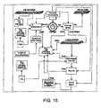
- FIG. 15 shows an exemplary flow diagram illustrating a strap preparation process, whereby a pressure sensitive adhesive (PSA) strip (or PSA drops) or other suitable adhesive material is formed on the undersides of the strap substrates, and the printed web is separated into individual straps.
- PSA pressure sensitive adhesive
- the printed web referred to as "die boards” in the drawing
- an electrically non-conductive PSA having suitable viscosity, electrical and drawdown characteristics is provided for application by a silkscreen tool or other application method available in the art.
- the silkscreen process applies a line or drops of PSA strips on the backsides and along the lengths of each of the strap substrates of the web.
- the PSA drops may be formed at appropriate positions on the inlay substrates, in preparation of attaching the straps to the inlay substrate.
- each strip 1600 contains a single row of RFID chips, DER strap pad patterns 714, and optionally, a PSA strip extending along the length and centerline on the underneath side of the long strip 1600. After the long strips 1600 have been formed, the longitudinal edges of each long strip 1600, and portions of the top surfaces of each RFID chip 708 adjacent to the RFID chip's contacts (if necessary), are dipped in DER ink and allowed to dry.
- the result of the dipping process, including the DER treated edges 1606, is shown in FIG. 17.
- the DER edge-treated strips 1600 are then cut into individual straps and stored in a magazine type applicator for subsequent processing.
- a top view of a DER edge treated strap 1800 after the cutting step is shown in FIG. 18.
- one or more of the strips may be rolled onto a reel and subsequently sold to customers or subsequently retrieved to complete the manufacture of the RFID inlays.
- FIG. 19 there is shown a flow diagram illustrating a strap mounting process for assembling the DER edge treated straps onto the inlay substrates of the inlay roll (see FIG. 14), according to an embodiment of the present invention.
- a finished roll of inlay substrates e.g. as obtained from the DER printing method described in connection with FIG. 13 above.
- the DER strap pad patterns of a strap are aligned with the antenna contact patterns of an inlay substrate on the inlay roll and, once aligned, the strap is temporarily secured to the inlay substrate by the PSA that was applied to the backside of the strap during the strap preparation method described above (see FIG. 15 and accompanying description).
- a top perspective view of the aligning and mounting process is shown in FIG. 20.
- the machine vision system may be adapted to determine the shape of the antenna, antenna contact patterns, or other shape or indicator, on the inlay substrate. Based on the identified shape or indicator, the pick and place process may be programmed to select from among different types of strap substrates. In this manner, different types of RFID inlays can be manufactured in the same process flow without requiring human intervention.
- the straps 1800 After the straps 1800 have been mounted to the roll of inlay substrates, small drops of epoxy may then be applied between the RFID chips 708 and strap substrates. After mounting, the strap pad patterns 714, antenna contact patterns 1402, antenna features 1400, and plating bar 1406 are all in electrical contact and ready for electroplating.
- the finished strap-mounted inlays are then rolled onto a reel and transferred to a plating station. Alternatively, the finished strap-mounted inlays are run to an electroplating station in a continuous process.
- FIG. 21 shows a flow diagram illustrating an electroplating process performed to complete the final RFID inlay shown in FIG. 7.
- a roll of finished strap-mounted inlays is configured for passing through a plating bath.
- the plating bath may be of the composition used to electroplate nickel (e.g. a nickel chloride salt) or other composition for depositing other types of metals (e.g. gold, silver, copper, etc.).
- a power supply is also configured to supply the appropriate electrical charge to the plating bar. Once the roll and power supply are properly configured, the roll of strap-mounted inlays are passed through the plating bath. During the process, all DER coated surfaces (and metal coated surfaces, e.g. the RFID chip contacts are plated.
- the finished RFID inlay roll is rinsed and allowed to dry. Then the plating bar is slit, for example using a laser cutter, so that the plating bar is no longer in electrical contact with the antenna on the inlay substrates. Finally, the finished RFID inlays are inspected to ensure that the plating process has been properly completed. Defective inlays are marked, separated and scrapped. Those RFID inlays that pass inspection are separated and sent to a laminator to form RFID labels.
- FIG. 21 shows various laminating methods that can be performed on the completed RFID inlays, to form RFID labels.
- the laminating method selected depends on the requirements of the finished label.
- the separated RFID inlays may be formed on a label substrate having a single PSA coating, formed on a label substrate having a double-sided PSA coating, or formed on a substrate not having a PSA coating.
- An exemplary finished RFID label 2200 is shown in FIG. 22.
- a filler layer 2205 e.g., comprised of a PSA material is formed over the electroplated surface of the RFID inlay 70 to protect the RFID inlay 70 and to provide a planar surface upon which other label layers may be formed.
- a lamination substrate 2206 is formed over the filler layer 2005.
- a printable substrate 2202 is formed over the lamination substrate 2206 and secured to the lamination substrate 2206 by an adhesive (e.g. PSA) layer 2204.
- the opposing side of the RFID inlay 70 may be secured to a release carrier 2210 by means of a second adhesive (e.g. PSA) layer 2208.
- FIG. 23 shows a cross-sectional drawing of an RFID inlay structure 2300, according to an alternative embodiment of the present invention.
- the RFID chip contacts 710 are placed in the recessed region so that the chip contacts 710 face the bottom of the recessed region, similar to a flip-chip mounting technique used in the semiconductor industry.
- a strap substrate 706 having a DER pattern like that shown in FIGS. 24A-C may be used.
- the DER pattern in FIG. 24 includes strap pad extensions 2400 that extend to the bottom of the recessed regions 820.
- the strap pad extensions 2400 may each be configured of an appropriate geometry that guarantees proper electrical contact to the chip contacts 710 regardless of how the chip contacts are oriented as they are assembled into the recessed regions 820.
- Other details concerning the printing, strap preparation, mounting, and electroplating processes are similar to those described above for manufacturing the RFID inlay 70 in FIG. 7 may be employed to complete the manufacture of the RFID inlay structure 2300 shown in FIG. 23.
- FIG. 25 shows a perspective drawing of a plurality of RFID inlay structures 2500, according to an embodiment of the present invention.
- DER antenna loop patterns 2502 are formed on the same substrate 2503 that the RFID chips 708 are mounted.
- the RFID chips are mounted to the substrate 2503 prior to forming the DER antenna loop patterns 2502.
- the antenna loop patterns 2502 are formed.
- the DER ink is also applied onto the RFID chip contacts 2504.
- One or more bus bars 2505 are also formed on the substrate 2503 using the DER ink to provide bus bar connections during an electroplating process. Similar to that explained above, the bus bar 2505 is separated from the antenna loops after the electroplating process.
- each of the RFID inlay structures 2500 are shown to have only a single loop, those of ordinary skill in the art will readily appreciate and understand that multiple loops may be formed. For example, by forming DER coated vias through the substrate 2503, additional loops can be formed on the opposite side of the substrate 2503. After the electroplating process, the RFID inlay structures 2500 may be cut into individual inlays and formed into RFID labels, similar to that described above.
- FIG. 26 is a simplified drawing of an inspection apparatus 2600, which may be used to inspect a strip, sheet, web or roll containing a plurality of RFID inlays, according to an embodiment of the present invention.
- the inspection apparatus 2600 is employed following the electroplating process described above (or other similar electroplating process), in a continuous manufacture/inspection operation; additionally or alternatively, the inspection apparatus 2600 may be employed at other stages and/or times in the manufacturing process.
- the inspection apparatus 2600 in FIG. 26 comprises an RFID reader 2602, a computer or workstation 2604, a printer (e.g. an ink jet printer) 2606 or labeling apparatus, and a transport apparatus (e.g. a conveyor) 2607.
- the RFID reader 2602 and the printer 2606 are connected to the computer/workstation 2604 by standard interfaces (e.g. serial, parallel, USB, RS-232, etc.).
- the RFID reader 2602 may comprise a single-mode reader, which is operable to read RFID inlays incorporating RFID chips of the same type.
- the reader 2602 may comprise a multi-mode reader or a multi-protocol reader configured to read RFID inlays incorporating different types of RFID chips.
- the terms "different types of RFID chips” or “different RFID chip types” are meant to include, but are not limited to, two or more RFID chips having one or more of the following distinguishing characteristics: size, shape, modulation protocol, encoding protocol, modulation frequency (e.g., low-frequency (LF) 125-135 kHz, high-frequency (HF) 13.56 MHz, ultra-high-frequency (UHF) 860-960 MHz, 3.45 GHz, 5.8 GHz, or other frequencies or frequency bands), class (e.g. Class 0, 1, etc.), generation (e.g. Gen. 1, 2, etc.), passive, active, backscatter, SAW (surface acoustic wave) based, CMOS-based, Title 21, read/write, read only, WORM (write once read many), and rewritable.
- modulation frequency e.g., low-frequency (LF) 125-135 kHz, high-frequency (HF) 13.56 MHz, ultra-high-frequency (UHF) 860-960 MHz
- a strip, sheet or web 2608 of RFID inlays (or, alternatively a roll of RFID inlays) 2610 incorporating RFID chips is fed into the inspection apparatus 2600 by the conveyor 2607 or other suitable transport mechanism.
- the RFID reader 2602 reads the RFID chips incorporated in the RFID inlays 2610.
- Each RFID chip of each RFID inlay 2610 is read and tested for functionality, frequency, transmission and reception capabilities, noise susceptibility, etc.
- the test/inspection measurements are collected and transmitted to the computer/workstation 2604 for processing and to determine whether the RFID chips of the respective RFID inlays 2610 are within predetermined and acceptable limits or satisfy other predetermined specifications.
- the serial numbers or other information stored in the RFID chips of those RFID inlays passing inspection are read by the reader 2602 and transmitted, via the computer/workstation 2604, to the printer 2606.
- the printer responds by printing the RFID inlays passing inspection with the serial numbers of the inlays' associated RFID chips, or other information (e.g. customer information, manufacture information, etc.).
- those RFID inlays containing RFID chips determined to be faulty or not in compliance with the predetermined test/inspection limits or specifications may be labeled as defective.
- the strip, sheet, web or roll of RFID inlays 2610 fed into the inspection apparatus 2600 may contain RFID inlays incorporating RFID chips of the same type or, alternatively, may contain RFID inlays incorporating RFID chips of different types.
- FIG. 27 is a top view drawing of an exemplary sheet 2700 of RFID inlays 2610 which can be inspected using the inspection apparatus 2600.
- the plurality of RFID inlays 2610 formed on the sheet 2700 incorporate different types of RFID chips.
- the labels "A" and "B” indicate that the sheet 2700 includes RFID inlays incorporating chips of type "A” or "B”, and are used generically to indicate any distinguishing characteristic.
- the manufacturing of the strips, sheets, webs or rolls of RFID inlays 2610 containing different RFID chip types may be manufactured according to the DER-based manufacturing methods described above.
- different chip-type specific, manufacturer or customer specific process parameters are provided to the DER printing tool. (See description of DER printing above.)
- the DER printing tool responds to the specified parameters to form the DER strap pad patterns on the strap substrates and/or the antenna patterns on the inlay substrates which are necessary to accommodate the different RFID chip types.
- the inspection apparatus and inspection methods of the present invention should be viewed as extending to inspecting strips, sheets, webs or rolls of RFID inlays incorporating different RFID chip types that have been manufactured with or without DER application and/or with or without the electroplating methods described above.
- the multi-mode reader 2602 comprises the multi-protocol XCI-DMU2 (Detector Module Unit) reader, which is commercially available reader available from XCI Incorporated, San Jose, CA.
- Other types of multi-protocol or multi-mode readers may also be used.
- any one of the multi-mode readers disclosed and/or claimed in commonly assigned U.S. Patent Nos. 6,107,910 , 6,433,671 , 6,531,957 , 6,580,358 , 6,950,009 and U.S. Patent Application No. 10/901,743 which are hereby incorporated into the present disclosure by reference, may be used.
- the terms "multi-mode reader” and “multi-protocol reader” are both meant to include within their meaning any RFID reader that is capable of reading two or more different types of RFID chips.
Landscapes
- Engineering & Computer Science (AREA)
- Microelectronics & Electronic Packaging (AREA)
- Computer Hardware Design (AREA)
- Physics & Mathematics (AREA)
- General Physics & Mathematics (AREA)
- Theoretical Computer Science (AREA)
- Manufacturing & Machinery (AREA)
- Details Of Aerials (AREA)
Applications Claiming Priority (2)
| Application Number | Priority Date | Filing Date | Title |
|---|---|---|---|
| US11/205,545 US20070040686A1 (en) | 2005-08-16 | 2005-08-16 | RFID inlays and methods of their manufacture |
| US11/263,888 US20070040688A1 (en) | 2005-08-16 | 2005-10-31 | RFID inlays and methods of their manufacture |
Publications (2)
| Publication Number | Publication Date |
|---|---|
| EP1755073A2 true EP1755073A2 (fr) | 2007-02-21 |
| EP1755073A3 EP1755073A3 (fr) | 2007-05-09 |
Family
ID=37499376
Family Applications (1)
| Application Number | Title | Priority Date | Filing Date |
|---|---|---|---|
| EP06119025A Withdrawn EP1755073A3 (fr) | 2005-08-16 | 2006-08-16 | RFID inlay et méthodes de fabrication |
Country Status (4)
| Country | Link |
|---|---|
| US (1) | US20070040688A1 (fr) |
| EP (1) | EP1755073A3 (fr) |
| JP (1) | JP2007052787A (fr) |
| CA (1) | CA2556133A1 (fr) |
Cited By (4)
| Publication number | Priority date | Publication date | Assignee | Title |
|---|---|---|---|---|
| US8299925B2 (en) | 2007-10-26 | 2012-10-30 | Fujitsu Limited | RFID tag and manufacturing method thereof |
| EP2587414A1 (fr) * | 2011-10-31 | 2013-05-01 | Tata Consultancy Services Limited | Étiquette passive RFID emballée destinée à des dispositifs de petite taille |
| EP2772874A1 (fr) * | 2013-02-27 | 2014-09-03 | Tata Consultancy Services Ltd. | Article activé d'étiquette RFID et procédé associé |
| CN114730365A (zh) * | 2019-11-26 | 2022-07-08 | 京瓷株式会社 | Rfid标签 |
Families Citing this family (19)
| Publication number | Priority date | Publication date | Assignee | Title |
|---|---|---|---|---|
| US20070040688A1 (en) | 2005-08-16 | 2007-02-22 | X-Cyte, Inc., A California Corporation | RFID inlays and methods of their manufacture |
| JP5034371B2 (ja) * | 2006-02-10 | 2012-09-26 | 富士通株式会社 | Rfidタグの製造方法およびrfidタグ |
| EP2023275B1 (fr) * | 2006-06-01 | 2011-04-27 | Murata Manufacturing Co. Ltd. | Dispositif à circuits intégrés radiofréquence et ses composant composite |
| US7701352B2 (en) * | 2006-11-22 | 2010-04-20 | Avery Dennison Corporation | RFID label with release liner window, and method of making |
| PL2126799T3 (pl) | 2007-03-23 | 2018-10-31 | Zih Corp. | Etykieta rfid o zmniejszonym rozstrajaniu |
| US8614506B1 (en) | 2007-10-03 | 2013-12-24 | Impinj, Inc. | RFID tags with bumped substrate, and apparatuses and methods for making |
| CN101874253B (zh) * | 2007-11-26 | 2013-01-02 | Nxp股份有限公司 | 制造天线或用于容纳集成电路的签带的方法、基板上的天线、集成电路的签带以及应答器 |
| US8056814B2 (en) * | 2008-02-27 | 2011-11-15 | Tagsys Sas | Combined EAS/RFID tag |
| BRPI0822605B1 (pt) | 2008-04-29 | 2019-04-02 | Compagnie Generale Des Etablissements Michelin | Dispositivo de identificação por radiofrequência, e, método para montagem de um dispositivo de identificação por radiofrequência. |
| DE102009027470A1 (de) * | 2009-07-06 | 2011-01-13 | Robert Bosch Gmbh | Ausbilden einer Kontaktfläche auf einer Leiterplatte |
| US8560262B2 (en) | 2010-06-18 | 2013-10-15 | Apple Inc. | Methods for manufacturing devices with flex circuits and radio-frequency cables |
| US10446728B2 (en) * | 2014-10-31 | 2019-10-15 | eLux, Inc. | Pick-and remove system and method for emissive display repair |
| US10418527B2 (en) * | 2014-10-31 | 2019-09-17 | eLux, Inc. | System and method for the fluidic assembly of emissive displays |
| EP3734511B1 (fr) * | 2017-12-29 | 2022-11-23 | Wu-Hsu Lin | Couche de préparation de module électronique et son procédé de fabrication |
| CN120197636A (zh) | 2018-11-15 | 2025-06-24 | 艾利丹尼森零售信息服务有限公司 | 可回收射频识别应答器部件及其生产方法 |
| KR102426308B1 (ko) * | 2018-12-04 | 2022-07-28 | 삼성전기주식회사 | 인쇄회로기판 및 이를 포함하는 모듈 |
| US20220230038A1 (en) * | 2019-04-22 | 2022-07-21 | Avery Dennison Retail Information Services Llc | Self-adhesive straps for rfid devices |
| EP4175824A1 (fr) * | 2021-08-30 | 2023-05-10 | BW Papersystems Stuttgart GmbH | Installation de conversion rfid et procédé de commande d'une pluralité de modules de distribution d'incrustations |
| US20240403594A1 (en) * | 2023-06-01 | 2024-12-05 | Ccl Label, Inc. | Antennas in radio frequency identification (rfid) tags |
Citations (6)
| Publication number | Priority date | Publication date | Assignee | Title |
|---|---|---|---|---|
| US5545291A (en) | 1993-12-17 | 1996-08-13 | The Regents Of The University Of California | Method for fabricating self-assembling microstructures |
| US6107910A (en) | 1996-11-29 | 2000-08-22 | X-Cyte, Inc. | Dual mode transmitter/receiver and decoder for RF transponder tags |
| US20020109929A1 (en) | 2001-02-14 | 2002-08-15 | Fujitsu Limited | Servo information detection method and disk apparatus using the same |
| US6582887B2 (en) | 2001-03-26 | 2003-06-24 | Daniel Luch | Electrically conductive patterns, antennas and methods of manufacture |
| US6867983B2 (en) | 2002-08-07 | 2005-03-15 | Avery Dennison Corporation | Radio frequency identification device and method |
| US20070040688A1 (en) | 2005-08-16 | 2007-02-22 | X-Cyte, Inc., A California Corporation | RFID inlays and methods of their manufacture |
Family Cites Families (39)
| Publication number | Priority date | Publication date | Assignee | Title |
|---|---|---|---|---|
| US3865699A (en) * | 1973-10-23 | 1975-02-11 | Int Nickel Co | Electrodeposition on non-conductive surfaces |
| JPS6033011A (ja) * | 1983-08-04 | 1985-02-20 | Mitsutoyo Mfg Co Ltd | 測定デ−タ合否判別装置 |
| US4900618A (en) * | 1986-11-07 | 1990-02-13 | Monsanto Company | Oxidation-resistant metal coatings |
| US4910072A (en) * | 1986-11-07 | 1990-03-20 | Monsanto Company | Selective catalytic activation of polymeric films |
| US5075037A (en) * | 1986-11-07 | 1991-12-24 | Monsanto Company | Selective catalytic activation of polymeric films |
| US5227223A (en) * | 1989-12-21 | 1993-07-13 | Monsanto Company | Fabricating metal articles from printed images |
| US5087510A (en) * | 1990-03-22 | 1992-02-11 | Monsanto Company | Electrolessly deposited metal holograms |
| DE19607212C1 (de) * | 1996-02-26 | 1997-04-10 | Richard Herbst | Verbundkörper, Verfahren und Kunststoff-Spritzgießwerkzeug zur Herstellung eines solchen |
| US5741430A (en) * | 1996-04-25 | 1998-04-21 | Lucent Technologies Inc. | Conductive adhesive bonding means |
| US6268796B1 (en) * | 1997-12-12 | 2001-07-31 | Alfred Gnadinger | Radio frequency identification transponder having integrated antenna |
| US6189208B1 (en) * | 1998-09-11 | 2001-02-20 | Polymer Flip Chip Corp. | Flip chip mounting technique |
| US6837438B1 (en) * | 1998-10-30 | 2005-01-04 | Hitachi Maxell, Ltd. | Non-contact information medium and communication system utilizing the same |
| US6203952B1 (en) * | 1999-01-14 | 2001-03-20 | 3M Innovative Properties Company | Imaged article on polymeric substrate |
| US6281038B1 (en) * | 1999-02-05 | 2001-08-28 | Alien Technology Corporation | Methods for forming assemblies |
| US6137452A (en) * | 1999-05-03 | 2000-10-24 | Centurion International, Inc. | Double shot antenna |
| US6246326B1 (en) * | 1999-05-05 | 2001-06-12 | Intermec Ip Corp. | Performance optimized smart label printer |
| US6784789B2 (en) * | 1999-07-08 | 2004-08-31 | Intermec Ip Corp. | Method and apparatus for verifying RFID tags |
| US6140146A (en) * | 1999-08-03 | 2000-10-31 | Intermec Ip Corp. | Automated RFID transponder manufacturing on flexible tape substrates |
| US6623579B1 (en) * | 1999-11-02 | 2003-09-23 | Alien Technology Corporation | Methods and apparatus for fluidic self assembly |
| JP2001134798A (ja) * | 1999-11-08 | 2001-05-18 | Nippon Chem Ind Co Ltd | 製品品質管理情報システム |
| US6451154B1 (en) * | 2000-02-18 | 2002-09-17 | Moore North America, Inc. | RFID manufacturing concepts |
| US6853087B2 (en) * | 2000-09-19 | 2005-02-08 | Nanopierce Technologies, Inc. | Component and antennae assembly in radio frequency identification devices |
| US6407669B1 (en) * | 2001-02-02 | 2002-06-18 | 3M Innovative Properties Company | RFID tag device and method of manufacturing |
| US6697248B1 (en) * | 2001-02-06 | 2004-02-24 | Daniel Luch | Electromagnetic interference shields and methods of manufacture |
| WO2002080637A1 (fr) * | 2001-04-02 | 2002-10-10 | Nashua Corporation | Elements de circuit possedant une trace conductrice enfouie et procedes de fabrication associes |
| US6606247B2 (en) * | 2001-05-31 | 2003-08-12 | Alien Technology Corporation | Multi-feature-size electronic structures |
| US6693541B2 (en) * | 2001-07-19 | 2004-02-17 | 3M Innovative Properties Co | RFID tag with bridge circuit assembly and methods of use |
| JP2003233652A (ja) * | 2002-02-12 | 2003-08-22 | Sharp Corp | 品質管理システム、品質管理方法、品質管理プログラム及び品質管理プログラムを記録した記録媒体 |
| US6770176B2 (en) * | 2002-08-02 | 2004-08-03 | Itn Energy Systems. Inc. | Apparatus and method for fracture absorption layer |
| US6940408B2 (en) * | 2002-12-31 | 2005-09-06 | Avery Dennison Corporation | RFID device and method of forming |
| US7225992B2 (en) * | 2003-02-13 | 2007-06-05 | Avery Dennison Corporation | RFID device tester and method |
| US7197279B2 (en) * | 2003-12-31 | 2007-03-27 | Wj Communications, Inc. | Multiprotocol RFID reader |
| JP4247129B2 (ja) * | 2004-01-19 | 2009-04-02 | 富士フイルム株式会社 | Rfidタグの検査装置 |
| US7158037B2 (en) * | 2004-03-22 | 2007-01-02 | Avery Dennison Corporation | Low cost method of producing radio frequency identification tags with straps without antenna patterning |
| JP2006031336A (ja) * | 2004-07-15 | 2006-02-02 | Fujitsu Ltd | Rfidタグの製造方法 |
| US7295117B2 (en) * | 2005-04-07 | 2007-11-13 | Avery Dennison | RFID device test thresholds systems and methods |
| US7749350B2 (en) * | 2005-04-27 | 2010-07-06 | Avery Dennison Retail Information Services | Webs and methods of making same |
| EP1920391B1 (fr) * | 2005-08-22 | 2016-11-16 | Avery Dennison Retail Information Services, LLC | Procede pour realiser des dispositifs rfid |
| US20070057795A1 (en) * | 2005-09-12 | 2007-03-15 | Wakahiro Kawai | Inspection method of RFID tag |
-
2005
- 2005-10-31 US US11/263,888 patent/US20070040688A1/en not_active Abandoned
-
2006
- 2006-08-15 JP JP2006221616A patent/JP2007052787A/ja active Pending
- 2006-08-15 CA CA002556133A patent/CA2556133A1/fr not_active Abandoned
- 2006-08-16 EP EP06119025A patent/EP1755073A3/fr not_active Withdrawn
Patent Citations (10)
| Publication number | Priority date | Publication date | Assignee | Title |
|---|---|---|---|---|
| US5545291A (en) | 1993-12-17 | 1996-08-13 | The Regents Of The University Of California | Method for fabricating self-assembling microstructures |
| US6107910A (en) | 1996-11-29 | 2000-08-22 | X-Cyte, Inc. | Dual mode transmitter/receiver and decoder for RF transponder tags |
| US6433671B1 (en) | 1996-11-29 | 2002-08-13 | X-Cyte, Inc. | Dual mode transmitter-receiver and decoder for RF transponder tags |
| US6531957B1 (en) | 1996-11-29 | 2003-03-11 | X-Cyte, Inc. | Dual mode transmitter-receiver and decoder for RF transponder tags |
| US6580358B1 (en) | 1996-11-29 | 2003-06-17 | X-Cyte, Inc. | Dual mode transmitter-receiver and decoder for RF transponder tags |
| US6950009B1 (en) | 1996-11-29 | 2005-09-27 | X-Cyte, Inc. | Dual mode transmitter/receiver and decoder for RF transponder units |
| US20020109929A1 (en) | 2001-02-14 | 2002-08-15 | Fujitsu Limited | Servo information detection method and disk apparatus using the same |
| US6582887B2 (en) | 2001-03-26 | 2003-06-24 | Daniel Luch | Electrically conductive patterns, antennas and methods of manufacture |
| US6867983B2 (en) | 2002-08-07 | 2005-03-15 | Avery Dennison Corporation | Radio frequency identification device and method |
| US20070040688A1 (en) | 2005-08-16 | 2007-02-22 | X-Cyte, Inc., A California Corporation | RFID inlays and methods of their manufacture |
Cited By (6)
| Publication number | Priority date | Publication date | Assignee | Title |
|---|---|---|---|---|
| US8299925B2 (en) | 2007-10-26 | 2012-10-30 | Fujitsu Limited | RFID tag and manufacturing method thereof |
| EP2053548B1 (fr) * | 2007-10-26 | 2013-04-10 | Fujitsu Limited | Étiquette RFID et procédé de fabrication correspondant |
| EP2587414A1 (fr) * | 2011-10-31 | 2013-05-01 | Tata Consultancy Services Limited | Étiquette passive RFID emballée destinée à des dispositifs de petite taille |
| EP2772874A1 (fr) * | 2013-02-27 | 2014-09-03 | Tata Consultancy Services Ltd. | Article activé d'étiquette RFID et procédé associé |
| CN114730365A (zh) * | 2019-11-26 | 2022-07-08 | 京瓷株式会社 | Rfid标签 |
| EP4068159A4 (fr) * | 2019-11-26 | 2023-12-20 | Kyocera Corporation | Étiquette rfid |
Also Published As
| Publication number | Publication date |
|---|---|
| CA2556133A1 (fr) | 2007-02-16 |
| US20070040688A1 (en) | 2007-02-22 |
| EP1755073A3 (fr) | 2007-05-09 |
| JP2007052787A (ja) | 2007-03-01 |
Similar Documents
| Publication | Publication Date | Title |
|---|---|---|
| EP1755073A2 (fr) | RFID inlay et méthodes de fabrication | |
| US7874493B2 (en) | Method of manufacturing RFID devices | |
| EP1755069A1 (fr) | Mince etiquette ci et procede de fabrication de celle-ci | |
| US6867983B2 (en) | Radio frequency identification device and method | |
| JP5881223B2 (ja) | プリント集積回路を含む無線デバイス並びにその製造及び使用方法 | |
| US8049626B2 (en) | RFID tag mounting circuit board | |
| CN104573791B (zh) | 嵌入式高频rfid | |
| US20070132594A1 (en) | Electronic device and fabrication method thereof | |
| US20070040686A1 (en) | RFID inlays and methods of their manufacture | |
| US20090051606A1 (en) | Electronic circuit module with built-in antenna and method for manufacturing the same | |
| US20080150725A1 (en) | Rfid label tag and method of manufacturing the same | |
| KR20050033833A (ko) | 무선 통신 매체 | |
| EP1746636A1 (fr) | Procédé de montage de puces de circuit intégré | |
| EP2023276B1 (fr) | Procédé de fabrication des étiquettes RFID | |
| EP2024910B1 (fr) | Procédé de fabrication de produits comprenant des transpondeurs | |
| CA2618036A1 (fr) | Mecanisme de fixation intermediaire et utilisation de ce mecanisme dans des transpondeurs rfid | |
| US8409928B2 (en) | Method for making contactless portable objects | |
| US7704790B2 (en) | Method of manufacturing a carrier member for electronic components | |
| KR101098289B1 (ko) | Rfid 태그, 이의 제작방법, 이를 이용한 패키징 구조체 및 제작방법 | |
| JP2007065867A (ja) | 非接触icタグ製造方法とその装置、および非接触icタグ | |
| KR20090036309A (ko) | 스마트 라벨 및 그 제조 방법 | |
| HK1129759B (en) | Manufacturing method for rfid tags | |
| KR20060132299A (ko) | 무선주파수 특성의 튜닝 방법 및 이를 사용하는 rfid태그 |
Legal Events
| Date | Code | Title | Description |
|---|---|---|---|
| PUAI | Public reference made under article 153(3) epc to a published international application that has entered the european phase |
Free format text: ORIGINAL CODE: 0009012 |
|
| AK | Designated contracting states |
Kind code of ref document: A2 Designated state(s): AT BE BG CH CY CZ DE DK EE ES FI FR GB GR HU IE IS IT LI LT LU LV MC NL PL PT RO SE SI SK TR |
|
| AX | Request for extension of the european patent |
Extension state: AL BA HR MK YU |
|
| PUAL | Search report despatched |
Free format text: ORIGINAL CODE: 0009013 |
|
| AK | Designated contracting states |
Kind code of ref document: A3 Designated state(s): AT BE BG CH CY CZ DE DK EE ES FI FR GB GR HU IE IS IT LI LT LU LV MC NL PL PT RO SE SI SK TR |
|
| AX | Request for extension of the european patent |
Extension state: AL BA HR MK YU |
|
| AKX | Designation fees paid | ||
| REG | Reference to a national code |
Ref country code: DE Ref legal event code: 8566 |
|
| STAA | Information on the status of an ep patent application or granted ep patent |
Free format text: STATUS: THE APPLICATION IS DEEMED TO BE WITHDRAWN |
|
| 18D | Application deemed to be withdrawn |
Effective date: 20071110 |