EP1755105A2 - Steuerschaltung für Farbflüssigkeitskristallanzeiger - Google Patents
Steuerschaltung für Farbflüssigkeitskristallanzeiger Download PDFInfo
- Publication number
- EP1755105A2 EP1755105A2 EP06125738A EP06125738A EP1755105A2 EP 1755105 A2 EP1755105 A2 EP 1755105A2 EP 06125738 A EP06125738 A EP 06125738A EP 06125738 A EP06125738 A EP 06125738A EP 1755105 A2 EP1755105 A2 EP 1755105A2
- Authority
- EP
- European Patent Office
- Prior art keywords
- time
- liquid crystal
- driver
- display according
- crystal display
- Prior art date
- Legal status (The legal status is an assumption and is not a legal conclusion. Google has not performed a legal analysis and makes no representation as to the accuracy of the status listed.)
- Withdrawn
Links
Images














Classifications
-
- G—PHYSICS
- G09—EDUCATION; CRYPTOGRAPHY; DISPLAY; ADVERTISING; SEALS
- G09G—ARRANGEMENTS OR CIRCUITS FOR CONTROL OF INDICATING DEVICES USING STATIC MEANS TO PRESENT VARIABLE INFORMATION
- G09G3/00—Control arrangements or circuits, of interest only in connection with visual indicators other than cathode-ray tubes
- G09G3/20—Control arrangements or circuits, of interest only in connection with visual indicators other than cathode-ray tubes for presentation of an assembly of a number of characters, e.g. a page, by composing the assembly by combination of individual elements arranged in a matrix no fixed position being assigned to or needed to be assigned to the individual characters or partial characters
- G09G3/34—Control arrangements or circuits, of interest only in connection with visual indicators other than cathode-ray tubes for presentation of an assembly of a number of characters, e.g. a page, by composing the assembly by combination of individual elements arranged in a matrix no fixed position being assigned to or needed to be assigned to the individual characters or partial characters by control of light from an independent source
- G09G3/36—Control arrangements or circuits, of interest only in connection with visual indicators other than cathode-ray tubes for presentation of an assembly of a number of characters, e.g. a page, by composing the assembly by combination of individual elements arranged in a matrix no fixed position being assigned to or needed to be assigned to the individual characters or partial characters by control of light from an independent source using liquid crystals
-
- G—PHYSICS
- G09—EDUCATION; CRYPTOGRAPHY; DISPLAY; ADVERTISING; SEALS
- G09G—ARRANGEMENTS OR CIRCUITS FOR CONTROL OF INDICATING DEVICES USING STATIC MEANS TO PRESENT VARIABLE INFORMATION
- G09G3/00—Control arrangements or circuits, of interest only in connection with visual indicators other than cathode-ray tubes
- G09G3/20—Control arrangements or circuits, of interest only in connection with visual indicators other than cathode-ray tubes for presentation of an assembly of a number of characters, e.g. a page, by composing the assembly by combination of individual elements arranged in a matrix no fixed position being assigned to or needed to be assigned to the individual characters or partial characters
- G09G3/34—Control arrangements or circuits, of interest only in connection with visual indicators other than cathode-ray tubes for presentation of an assembly of a number of characters, e.g. a page, by composing the assembly by combination of individual elements arranged in a matrix no fixed position being assigned to or needed to be assigned to the individual characters or partial characters by control of light from an independent source
- G09G3/36—Control arrangements or circuits, of interest only in connection with visual indicators other than cathode-ray tubes for presentation of an assembly of a number of characters, e.g. a page, by composing the assembly by combination of individual elements arranged in a matrix no fixed position being assigned to or needed to be assigned to the individual characters or partial characters by control of light from an independent source using liquid crystals
- G09G3/3611—Control of matrices with row and column drivers
- G09G3/3685—Details of drivers for data electrodes
- G09G3/3688—Details of drivers for data electrodes suitable for active matrices only
-
- G—PHYSICS
- G02—OPTICS
- G02F—OPTICAL DEVICES OR ARRANGEMENTS FOR THE CONTROL OF LIGHT BY MODIFICATION OF THE OPTICAL PROPERTIES OF THE MEDIA OF THE ELEMENTS INVOLVED THEREIN; NON-LINEAR OPTICS; FREQUENCY-CHANGING OF LIGHT; OPTICAL LOGIC ELEMENTS; OPTICAL ANALOGUE/DIGITAL CONVERTERS
- G02F1/00—Devices or arrangements for the control of the intensity, colour, phase, polarisation or direction of light arriving from an independent light source, e.g. switching, gating or modulating; Non-linear optics
- G02F1/01—Devices or arrangements for the control of the intensity, colour, phase, polarisation or direction of light arriving from an independent light source, e.g. switching, gating or modulating; Non-linear optics for the control of the intensity, phase, polarisation or colour
- G02F1/13—Devices or arrangements for the control of the intensity, colour, phase, polarisation or direction of light arriving from an independent light source, e.g. switching, gating or modulating; Non-linear optics for the control of the intensity, phase, polarisation or colour based on liquid crystals, e.g. single liquid crystal display cells
- G02F1/133—Constructional arrangements; Operation of liquid crystal cells; Circuit arrangements
- G02F1/1333—Constructional arrangements; Manufacturing methods
- G02F1/1345—Conductors connecting electrodes to cell terminals
- G02F1/13452—Conductors connecting driver circuitry and terminals of panels
-
- G—PHYSICS
- G09—EDUCATION; CRYPTOGRAPHY; DISPLAY; ADVERTISING; SEALS
- G09G—ARRANGEMENTS OR CIRCUITS FOR CONTROL OF INDICATING DEVICES USING STATIC MEANS TO PRESENT VARIABLE INFORMATION
- G09G3/00—Control arrangements or circuits, of interest only in connection with visual indicators other than cathode-ray tubes
- G09G3/20—Control arrangements or circuits, of interest only in connection with visual indicators other than cathode-ray tubes for presentation of an assembly of a number of characters, e.g. a page, by composing the assembly by combination of individual elements arranged in a matrix no fixed position being assigned to or needed to be assigned to the individual characters or partial characters
- G09G3/2007—Display of intermediate tones
- G09G3/2011—Display of intermediate tones by amplitude modulation
-
- G—PHYSICS
- G09—EDUCATION; CRYPTOGRAPHY; DISPLAY; ADVERTISING; SEALS
- G09G—ARRANGEMENTS OR CIRCUITS FOR CONTROL OF INDICATING DEVICES USING STATIC MEANS TO PRESENT VARIABLE INFORMATION
- G09G3/00—Control arrangements or circuits, of interest only in connection with visual indicators other than cathode-ray tubes
- G09G3/20—Control arrangements or circuits, of interest only in connection with visual indicators other than cathode-ray tubes for presentation of an assembly of a number of characters, e.g. a page, by composing the assembly by combination of individual elements arranged in a matrix no fixed position being assigned to or needed to be assigned to the individual characters or partial characters
- G09G3/34—Control arrangements or circuits, of interest only in connection with visual indicators other than cathode-ray tubes for presentation of an assembly of a number of characters, e.g. a page, by composing the assembly by combination of individual elements arranged in a matrix no fixed position being assigned to or needed to be assigned to the individual characters or partial characters by control of light from an independent source
- G09G3/36—Control arrangements or circuits, of interest only in connection with visual indicators other than cathode-ray tubes for presentation of an assembly of a number of characters, e.g. a page, by composing the assembly by combination of individual elements arranged in a matrix no fixed position being assigned to or needed to be assigned to the individual characters or partial characters by control of light from an independent source using liquid crystals
- G09G3/3611—Control of matrices with row and column drivers
- G09G3/3648—Control of matrices with row and column drivers using an active matrix
-
- G—PHYSICS
- G02—OPTICS
- G02F—OPTICAL DEVICES OR ARRANGEMENTS FOR THE CONTROL OF LIGHT BY MODIFICATION OF THE OPTICAL PROPERTIES OF THE MEDIA OF THE ELEMENTS INVOLVED THEREIN; NON-LINEAR OPTICS; FREQUENCY-CHANGING OF LIGHT; OPTICAL LOGIC ELEMENTS; OPTICAL ANALOGUE/DIGITAL CONVERTERS
- G02F1/00—Devices or arrangements for the control of the intensity, colour, phase, polarisation or direction of light arriving from an independent light source, e.g. switching, gating or modulating; Non-linear optics
- G02F1/01—Devices or arrangements for the control of the intensity, colour, phase, polarisation or direction of light arriving from an independent light source, e.g. switching, gating or modulating; Non-linear optics for the control of the intensity, phase, polarisation or colour
- G02F1/13—Devices or arrangements for the control of the intensity, colour, phase, polarisation or direction of light arriving from an independent light source, e.g. switching, gating or modulating; Non-linear optics for the control of the intensity, phase, polarisation or colour based on liquid crystals, e.g. single liquid crystal display cells
- G02F1/133—Constructional arrangements; Operation of liquid crystal cells; Circuit arrangements
- G02F1/1333—Constructional arrangements; Manufacturing methods
- G02F1/1345—Conductors connecting electrodes to cell terminals
-
- G—PHYSICS
- G09—EDUCATION; CRYPTOGRAPHY; DISPLAY; ADVERTISING; SEALS
- G09G—ARRANGEMENTS OR CIRCUITS FOR CONTROL OF INDICATING DEVICES USING STATIC MEANS TO PRESENT VARIABLE INFORMATION
- G09G2300/00—Aspects of the constitution of display devices
- G09G2300/04—Structural and physical details of display devices
- G09G2300/0404—Matrix technologies
- G09G2300/0408—Integration of the drivers onto the display substrate
-
- G—PHYSICS
- G09—EDUCATION; CRYPTOGRAPHY; DISPLAY; ADVERTISING; SEALS
- G09G—ARRANGEMENTS OR CIRCUITS FOR CONTROL OF INDICATING DEVICES USING STATIC MEANS TO PRESENT VARIABLE INFORMATION
- G09G2300/00—Aspects of the constitution of display devices
- G09G2300/08—Active matrix structure, i.e. with use of active elements, inclusive of non-linear two terminal elements, in the pixels together with light emitting or modulating elements
- G09G2300/0876—Supplementary capacities in pixels having special driving circuits and electrodes instead of being connected to common electrode or ground; Use of additional capacitively coupled compensation electrodes
-
- G—PHYSICS
- G09—EDUCATION; CRYPTOGRAPHY; DISPLAY; ADVERTISING; SEALS
- G09G—ARRANGEMENTS OR CIRCUITS FOR CONTROL OF INDICATING DEVICES USING STATIC MEANS TO PRESENT VARIABLE INFORMATION
- G09G2310/00—Command of the display device
- G09G2310/02—Addressing, scanning or driving the display screen or processing steps related thereto
- G09G2310/0264—Details of driving circuits
- G09G2310/027—Details of drivers for data electrodes, the drivers handling digital grey scale data, e.g. use of D/A converters
-
- G—PHYSICS
- G09—EDUCATION; CRYPTOGRAPHY; DISPLAY; ADVERTISING; SEALS
- G09G—ARRANGEMENTS OR CIRCUITS FOR CONTROL OF INDICATING DEVICES USING STATIC MEANS TO PRESENT VARIABLE INFORMATION
- G09G2310/00—Command of the display device
- G09G2310/02—Addressing, scanning or driving the display screen or processing steps related thereto
- G09G2310/0264—Details of driving circuits
- G09G2310/0289—Details of voltage level shifters arranged for use in a driving circuit
-
- G—PHYSICS
- G09—EDUCATION; CRYPTOGRAPHY; DISPLAY; ADVERTISING; SEALS
- G09G—ARRANGEMENTS OR CIRCUITS FOR CONTROL OF INDICATING DEVICES USING STATIC MEANS TO PRESENT VARIABLE INFORMATION
- G09G2310/00—Command of the display device
- G09G2310/02—Addressing, scanning or driving the display screen or processing steps related thereto
- G09G2310/0264—Details of driving circuits
- G09G2310/0297—Special arrangements with multiplexing or demultiplexing of display data in the drivers for data electrodes, in a pre-processing circuitry delivering display data to said drivers or in the matrix panel, e.g. multiplexing plural data signals to one D/A converter or demultiplexing the D/A converter output to multiple columns
-
- G—PHYSICS
- G09—EDUCATION; CRYPTOGRAPHY; DISPLAY; ADVERTISING; SEALS
- G09G—ARRANGEMENTS OR CIRCUITS FOR CONTROL OF INDICATING DEVICES USING STATIC MEANS TO PRESENT VARIABLE INFORMATION
- G09G2310/00—Command of the display device
- G09G2310/06—Details of flat display driving waveforms
-
- G—PHYSICS
- G09—EDUCATION; CRYPTOGRAPHY; DISPLAY; ADVERTISING; SEALS
- G09G—ARRANGEMENTS OR CIRCUITS FOR CONTROL OF INDICATING DEVICES USING STATIC MEANS TO PRESENT VARIABLE INFORMATION
- G09G2310/00—Command of the display device
- G09G2310/06—Details of flat display driving waveforms
- G09G2310/066—Waveforms comprising a gently increasing or decreasing portion, e.g. ramp
-
- G—PHYSICS
- G09—EDUCATION; CRYPTOGRAPHY; DISPLAY; ADVERTISING; SEALS
- G09G—ARRANGEMENTS OR CIRCUITS FOR CONTROL OF INDICATING DEVICES USING STATIC MEANS TO PRESENT VARIABLE INFORMATION
- G09G2320/00—Control of display operating conditions
- G09G2320/02—Improving the quality of display appearance
- G09G2320/0209—Crosstalk reduction, i.e. to reduce direct or indirect influences of signals directed to a certain pixel of the displayed image on other pixels of said image, inclusive of influences affecting pixels in different frames or fields or sub-images which constitute a same image, e.g. left and right images of a stereoscopic display
-
- G—PHYSICS
- G09—EDUCATION; CRYPTOGRAPHY; DISPLAY; ADVERTISING; SEALS
- G09G—ARRANGEMENTS OR CIRCUITS FOR CONTROL OF INDICATING DEVICES USING STATIC MEANS TO PRESENT VARIABLE INFORMATION
- G09G2320/00—Control of display operating conditions
- G09G2320/02—Improving the quality of display appearance
- G09G2320/0223—Compensation for problems related to R-C delay and attenuation in electrodes of matrix panels, e.g. in gate electrodes or on-substrate video signal electrodes
-
- G—PHYSICS
- G09—EDUCATION; CRYPTOGRAPHY; DISPLAY; ADVERTISING; SEALS
- G09G—ARRANGEMENTS OR CIRCUITS FOR CONTROL OF INDICATING DEVICES USING STATIC MEANS TO PRESENT VARIABLE INFORMATION
- G09G2330/00—Aspects of power supply; Aspects of display protection and defect management
- G09G2330/02—Details of power systems and of start or stop of display operation
- G09G2330/021—Power management, e.g. power saving
-
- G—PHYSICS
- G09—EDUCATION; CRYPTOGRAPHY; DISPLAY; ADVERTISING; SEALS
- G09G—ARRANGEMENTS OR CIRCUITS FOR CONTROL OF INDICATING DEVICES USING STATIC MEANS TO PRESENT VARIABLE INFORMATION
- G09G3/00—Control arrangements or circuits, of interest only in connection with visual indicators other than cathode-ray tubes
- G09G3/20—Control arrangements or circuits, of interest only in connection with visual indicators other than cathode-ray tubes for presentation of an assembly of a number of characters, e.g. a page, by composing the assembly by combination of individual elements arranged in a matrix no fixed position being assigned to or needed to be assigned to the individual characters or partial characters
- G09G3/34—Control arrangements or circuits, of interest only in connection with visual indicators other than cathode-ray tubes for presentation of an assembly of a number of characters, e.g. a page, by composing the assembly by combination of individual elements arranged in a matrix no fixed position being assigned to or needed to be assigned to the individual characters or partial characters by control of light from an independent source
- G09G3/36—Control arrangements or circuits, of interest only in connection with visual indicators other than cathode-ray tubes for presentation of an assembly of a number of characters, e.g. a page, by composing the assembly by combination of individual elements arranged in a matrix no fixed position being assigned to or needed to be assigned to the individual characters or partial characters by control of light from an independent source using liquid crystals
- G09G3/3607—Control arrangements or circuits, of interest only in connection with visual indicators other than cathode-ray tubes for presentation of an assembly of a number of characters, e.g. a page, by composing the assembly by combination of individual elements arranged in a matrix no fixed position being assigned to or needed to be assigned to the individual characters or partial characters by control of light from an independent source using liquid crystals for displaying colours or for displaying grey scales with a specific pixel layout, e.g. using sub-pixels
-
- G—PHYSICS
- G09—EDUCATION; CRYPTOGRAPHY; DISPLAY; ADVERTISING; SEALS
- G09G—ARRANGEMENTS OR CIRCUITS FOR CONTROL OF INDICATING DEVICES USING STATIC MEANS TO PRESENT VARIABLE INFORMATION
- G09G3/00—Control arrangements or circuits, of interest only in connection with visual indicators other than cathode-ray tubes
- G09G3/20—Control arrangements or circuits, of interest only in connection with visual indicators other than cathode-ray tubes for presentation of an assembly of a number of characters, e.g. a page, by composing the assembly by combination of individual elements arranged in a matrix no fixed position being assigned to or needed to be assigned to the individual characters or partial characters
- G09G3/34—Control arrangements or circuits, of interest only in connection with visual indicators other than cathode-ray tubes for presentation of an assembly of a number of characters, e.g. a page, by composing the assembly by combination of individual elements arranged in a matrix no fixed position being assigned to or needed to be assigned to the individual characters or partial characters by control of light from an independent source
- G09G3/36—Control arrangements or circuits, of interest only in connection with visual indicators other than cathode-ray tubes for presentation of an assembly of a number of characters, e.g. a page, by composing the assembly by combination of individual elements arranged in a matrix no fixed position being assigned to or needed to be assigned to the individual characters or partial characters by control of light from an independent source using liquid crystals
- G09G3/3611—Control of matrices with row and column drivers
- G09G3/3614—Control of polarity reversal in general
-
- G—PHYSICS
- G09—EDUCATION; CRYPTOGRAPHY; DISPLAY; ADVERTISING; SEALS
- G09G—ARRANGEMENTS OR CIRCUITS FOR CONTROL OF INDICATING DEVICES USING STATIC MEANS TO PRESENT VARIABLE INFORMATION
- G09G3/00—Control arrangements or circuits, of interest only in connection with visual indicators other than cathode-ray tubes
- G09G3/20—Control arrangements or circuits, of interest only in connection with visual indicators other than cathode-ray tubes for presentation of an assembly of a number of characters, e.g. a page, by composing the assembly by combination of individual elements arranged in a matrix no fixed position being assigned to or needed to be assigned to the individual characters or partial characters
- G09G3/34—Control arrangements or circuits, of interest only in connection with visual indicators other than cathode-ray tubes for presentation of an assembly of a number of characters, e.g. a page, by composing the assembly by combination of individual elements arranged in a matrix no fixed position being assigned to or needed to be assigned to the individual characters or partial characters by control of light from an independent source
- G09G3/36—Control arrangements or circuits, of interest only in connection with visual indicators other than cathode-ray tubes for presentation of an assembly of a number of characters, e.g. a page, by composing the assembly by combination of individual elements arranged in a matrix no fixed position being assigned to or needed to be assigned to the individual characters or partial characters by control of light from an independent source using liquid crystals
- G09G3/3611—Control of matrices with row and column drivers
- G09G3/3648—Control of matrices with row and column drivers using an active matrix
- G09G3/3655—Details of drivers for counter electrodes, e.g. common electrodes for pixel capacitors or supplementary storage capacitors
-
- G—PHYSICS
- G09—EDUCATION; CRYPTOGRAPHY; DISPLAY; ADVERTISING; SEALS
- G09G—ARRANGEMENTS OR CIRCUITS FOR CONTROL OF INDICATING DEVICES USING STATIC MEANS TO PRESENT VARIABLE INFORMATION
- G09G3/00—Control arrangements or circuits, of interest only in connection with visual indicators other than cathode-ray tubes
- G09G3/20—Control arrangements or circuits, of interest only in connection with visual indicators other than cathode-ray tubes for presentation of an assembly of a number of characters, e.g. a page, by composing the assembly by combination of individual elements arranged in a matrix no fixed position being assigned to or needed to be assigned to the individual characters or partial characters
- G09G3/34—Control arrangements or circuits, of interest only in connection with visual indicators other than cathode-ray tubes for presentation of an assembly of a number of characters, e.g. a page, by composing the assembly by combination of individual elements arranged in a matrix no fixed position being assigned to or needed to be assigned to the individual characters or partial characters by control of light from an independent source
- G09G3/36—Control arrangements or circuits, of interest only in connection with visual indicators other than cathode-ray tubes for presentation of an assembly of a number of characters, e.g. a page, by composing the assembly by combination of individual elements arranged in a matrix no fixed position being assigned to or needed to be assigned to the individual characters or partial characters by control of light from an independent source using liquid crystals
- G09G3/3611—Control of matrices with row and column drivers
- G09G3/3648—Control of matrices with row and column drivers using an active matrix
- G09G3/3666—Control of matrices with row and column drivers using an active matrix with the matrix divided into sections
-
- G—PHYSICS
- G09—EDUCATION; CRYPTOGRAPHY; DISPLAY; ADVERTISING; SEALS
- G09G—ARRANGEMENTS OR CIRCUITS FOR CONTROL OF INDICATING DEVICES USING STATIC MEANS TO PRESENT VARIABLE INFORMATION
- G09G3/00—Control arrangements or circuits, of interest only in connection with visual indicators other than cathode-ray tubes
- G09G3/20—Control arrangements or circuits, of interest only in connection with visual indicators other than cathode-ray tubes for presentation of an assembly of a number of characters, e.g. a page, by composing the assembly by combination of individual elements arranged in a matrix no fixed position being assigned to or needed to be assigned to the individual characters or partial characters
- G09G3/34—Control arrangements or circuits, of interest only in connection with visual indicators other than cathode-ray tubes for presentation of an assembly of a number of characters, e.g. a page, by composing the assembly by combination of individual elements arranged in a matrix no fixed position being assigned to or needed to be assigned to the individual characters or partial characters by control of light from an independent source
- G09G3/36—Control arrangements or circuits, of interest only in connection with visual indicators other than cathode-ray tubes for presentation of an assembly of a number of characters, e.g. a page, by composing the assembly by combination of individual elements arranged in a matrix no fixed position being assigned to or needed to be assigned to the individual characters or partial characters by control of light from an independent source using liquid crystals
- G09G3/3611—Control of matrices with row and column drivers
- G09G3/3696—Generation of voltages supplied to electrode drivers
Definitions
- the invention relates to a liquid crystal display (LCD) and, more particularly, to a matrix type liquid crystal display in which a driver circuit to apply a signal potential to each pixel is provided as an external circuit of a liquid crystal display panel.
- LCD liquid crystal display
- a driver circuit to apply a signal potential to each pixel is provided as an external circuit of a liquid crystal display panel.
- a matrix type is a main stream.
- the matrix type liquid crystal display is excellent in terms of a response speed and an image quality and is a display apparatus suitable for realization of a recent color display.
- a non-linear element such as transistor, diode, or the like is used in each pixel of a liquid crystal display panel.
- it has a structure such that a thin film transistor (TFT) is formed on a glass substrate.
- TFT thin film transistor
- the general driver IC is used for the signal lines in which the total number of output pins is determined by the display system is used, a situation such that a remainder occurs in the number of pins of the driver IC occurs.
- a surplus pin portion among the output pins of a driver IC 101 becomes a surplus connecting region which does not contribute to the image display and occupies right and left frame portions of a liquid crystal display panel 102, so that a size in the horizontal direction of the liquid crystal display panel 102 increases. Thus, it becomes an obstacle for realization of a compact size of the whole liquid crystal display.
- the driver IC 101 is connected to each signal line in connecting portions 104 on the liquid crystal display panel 102 through flexible cables 103.
- the invention is made in consideration of the above problems and it is an object of the invention to provide a liquid crystal display which can realize a narrow width in the horizontal direction of a liquid crystal display panel in case of using an external driver IC.
- a liquid crystal display comprising: a display portion in which a plurality of pixels are two-dimensionally arranged at intersecting points of gate lines as many as a plurality of rows and signal lines as many as a plurality of columns which are wired in a matrix shape; and a plurality of driver circuits for applying a signal potential to each pixel of the display portion through the signal lines of a plurality of columns, wherein the number of output terminals of each of the plurality of driver circuits is set to a measure of the total number of signal lines of a plurality of columns.
- Fig. 2 is a wiring diagram of a liquid crystal display portion in a matrix type liquid crystal display according to the invention.
- the matrix type liquid crystal display has a structure such that gate lines 11-1, 11-2, 11-3, ... as many as a plurality of rows and signal lines 12-1, 12-2, 12-3, ... as many as a plurality of columns are wired in a matrix form onto the surface of liquid crystal and a back light is arranged on the back side of the liquid crystal. Intersecting points of the gate lines 11-1, 11-2, 11-3, ... and signal lines 12-1, 12-2, 12-3, ... become pixels and form a liquid crystal display panel (display portion) 10. A construction of the pixels will be described hereinlater.
- each of the gate lines 11-1, 11-2, 11-3, ... as many as a plurality of rows is connected to each output terminal of the corresponding row of a vertical driving circuit 13.
- the vertical driving circuit 13 is formed by a thin film transistor onto the same substrate as that of the liquid crystal display panel and performs a vertical scan by supplying scanning pulses in order to the gate lines 11-1, 11-2, 11-3, ... and selecting each pixel on a row unit basis.
- the vertical driving circuit 13 is arranged on only one side of the liquid crystal display panel 10, obviously, it can be arranged on both sides of the liquid crystal display panel 10.
- a plurality of driver ICs 14-1, 14-2, 14-3, ... for applying a predetermined voltage according to image data to the signal lines 12-1, 12-2, 12-3, ... are provided as external circuits of the liquid crystal display panel 10.
- Digital image data which enables a display of, for example, 8 or more gradations and 512 or more colors is inputted to the plurality of driver ICs 14-1, 14-2, 14-3, ....
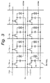
- Fig. 3 is a circuit constructional diagram of the pixels. As will be obviously understood from Fig. 3, each pixel 20 is constructed by a thin film transistor 21, an additional capacitor 22, and a liquid crystal capacitor 23. A gate electrode of the thin film transistor 21 is connected to the gate lines 11-1, 11-2, 11-3, ... and a source electrode is connected to the signal lines 12-1, 12-2, 12-3, ..., respectively.
- the liquid crystal capacitor 23 denotes a capacitance which occurs between a pixel electrode that is formed by the thin film transistor 21 and a counter electrode which is formed in correspondence to it.
- An electric potential which is held in the pixel electrode is written by an electric potential of "H” or "L".
- H indicates a high voltage writing state and "L” shows a low voltage writing state.
- an electric potential (common potential VCOM) of the counter electrode is set to, for example, a DC potential of 6V.
- VCOM common potential
- the AC driving can reduce a polarizing function of a liquid crystal molecule and charging of the liquid crystal molecule or charging of an insulating film existing on the electrode surface can be prevented.
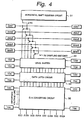
- Fig. 4 is a block diagram showing an example of an internal construction of the driver ICs 14-1, 14-2, 14-3, ....
- the driver ICs have a horizontal shift register circuit 31, sampling switches 32, a level shifter 33, a data latch circuit 34, and a digital/analog converting circuit 35.
- digital image data data1 to data5 of five bits and power source voltages Vdd and Vss are fetched from both sides in the shift direction of the horizontal shift register circuit 31.
- the horizontal shift register circuit 31 performs a horizontal scan (column scan) by sequentially generating horizontal scanning pulses.
- the sampling switches in the sampling switches 32 sequentially sample the input digital image data data1 to data5 in response to the horizontal scanning pulses from the horizontal shift register circuit 31.
- the level shifter 33 boosts the digital data of, for example, 5V sampled by the sampling switches 32 to digital data of a liquid crystal driving voltage.
- the data latch circuit 34 is a memory to accumulate the digital data boosted by the level shifter 33 by an amount of one horizontal period.
- the digital/analog converting circuit 35 converts the digital data of one horizontal period which is outputted from the data latch circuit 34 into an analog signal and outputs it.
- the invention is characterized by a construction of a connecting portion between each of the signal lines 12-1, 12-2, 12-3, ... of the liquid crystal display panel 10 and the output pin (output terminal) of each of the plurality of the driver ICs 14-1, 14-2, 14-3, ....
- a liquid crystal display of, for example, the XGA display system will be first described by using Fig. 5.
- This liquid crystal display is the subject of European patent application number 99 909 300 , from which the present application has been divided.
- driver ICs each having, for example, 120 output pins are used as driver ICs 14-1, 14-2, 14-3, ... and arranged in order in correspondence to the signal lines 12-1, 12-2, 12-3, ....
- a driver IC holding the 72 signal lines of such a fraction a driver IC having 72 output pins is used instead of the general driver IC having the 120 output pins, and total 26 driver ICs 14-1, 14-2, 14-3, ..., and 14-26 including such a driver IC are arranged in order in the horizontal direction.
- the driver IC having 72 output pins is used as, for example, a driver IC 14-26 which is arranged in the 26th order. That is, although the number of signal lines which are allocated to each of the other 25 driver ICs 14-1, 14-2, 14-3, ..., and 14-25 is equal to 120, the number of signal lines which are allocated to the 26th driver IC 14-26 is equal to 72.
- the output pins of the 26 driver ICs 14-1, 14-2, 14-3, ..., and 14-26 arranged in this manner are connected to the signal lines 12-1, 12-2, 12-3, ... in connecting portions 16 on the liquid crystal display panel 10 through flexible cables 15, respectively, and apply a predetermined voltage to each pixel through the signal lines 12-1, 12-2, 12-3, ....
- the general driver ICs in which the numbers of output pins are the same as driver ICs 14-1, 14-2, 14-3, ..., when these driver ICs are sequentially arranged with a correspondence relation with each of the signal lines 12-1, 12-2, 12-3, ..., if a fraction occurs in the signal lines, by setting the number of output pins of one of the driver ICs 14-1, 14-2, 14-3, ... to such a fraction, no fraction finally occurs in the signal lines and the output pins of the driver ICs can be connected to the signal lines without causing a remainder. Thus, a surplus connecting region which does not contribute to the image display does not occur on the liquid crystal display panel 10.
- the position where the driver IC holding the fraction of the signal lines is arranged is set to the end (the 26th IC in the drawing) in the drawing, it is not limited to the end position and can be arranged at any position.
- the numerical values shown in the drawing are a mere example and the device is not limited to these numerical values.
- the liquid crystal display panel 10 has 1024 (namely, total 3072) signal lines 12-1, 12-2, 12-3, ... every color of R, G, and B as mentioned above.
- 1024 namely, total 3072
- the driver ICs 14-1, 14-2, 14-3, ... are arranged for the 3072 signal lines 12-1, 12-2, 12-3, ..., in this instance, the number of output pins of the driver ICs 14-1, 14-2, 14-3, ... is set to a measure of the total number (namely, the number of horizontal display dots) of signal lines 12-1, 12-2, 12-3, ....
- the output pins of the six driver ICs 14-1, 14-2, 14-3, ..., and 14-6 arranged in this manner are connected to the signal lines 12-1, 12-2, 12-3, ... in the connecting portions 16 on the liquid crystal display panel 10 through the flexible cables 15 and the driver ICs apply a predetermined voltage to each pixel through the signal lines 12-1, 1-2, 12-3, ....
- the number of output pins of the driver ICs 14-1, 14-2, 14-3, ... is set, the number of output pins is set to the measure of the total number of signal lines 12-1, 12-2, 12-3, ... and the driver ICs of the number which is determined by the number of output pins are arranged, so that no fraction occurs in the signal lines and the output pins of the driver IC can be connected to the signal lines without causing a remainder.
- a surplus connecting region which does not contribute to the image display does not occur in the liquid crystal display panel 10.
- the numerical values shown in the embodiment are a mere example and the invention is not limited to these numerical values.
- the embodiment has been described with respect to the case where the invention is applied to the XGA (1024 pixels x 768 pixels) display, the invention can be also applied to other display systems, for example, an NTSC (640 pixels x 480 pixels) display, a VGA (800 pixels x 600 pixels) display, an SXGA (1280 pixels x 1024 pixels) display, and a UXGA (1600 pixels x 1400 pixels) display.
- NTSC 640 pixels x 480 pixels
- VGA 800 pixels x 600 pixels
- SXGA (1280 pixels x 1024 pixels
- UXGA (1600 pixels x 1400 pixels
- the invention can be also applied to a liquid crystal display in which there is no one-to-one correspondence relation. That is, in a liquid crystal display using what is called a time-divisional driving method, there is no one-to-one correspondence relation between the output pins of the external driver IC and the signal lines and the invention can be applied to such a kind of liquid crystal display.
- the time-divisional driving method is a driving method whereby a plurality of signal lines are set to one unit (block), signals which are supplied to the plurality of signal lines in one divided block are time-sequentially outputted from the driver IC, time-divisional switches are provided for the liquid crystal display panel while a plurality of signal lines are set to one unit, the time-sequential signals which are outputted from the driver IC are time-divided by the time-divisional switches and sequentially supplied to the plurality of signal lines.
- the number of output pins of the driver IC can be reduced by using the time-divisional driving method.
- Fig. 7 is a wiring diagram of a liquid crystal display portion in a matrix type liquid crystal display using the time-divisional driving method.
- the matrix type liquid crystal display has a structure such that gate lines 41-1, 41-2, 41-3, ... as many as a plurality of rows and signal lines 42-1, 42-2, 42-3, ... as many as a plurality of columns are wired in a matrix shape on the surface of liquid crystal and a back light is arranged on the backside of the liquid crystal. Intersecting points between the gate lines 41-1, 41-2, 41-3, ... and the signal lines 42-1, 42-2, 42-3, ... become pixels and form a liquid crystal display panel 40.
- the pixels have a construction shown in, for example, Fig. 3.
- each of the gate lines 41-1, 41-2, 41-3, ... of a plurality of rows is connected to each output terminal of the corresponding row of a vertical driving circuit 43, respectively.
- the vertical driving circuit 43 is formed by a thin film transistor onto the same substrate as that of the liquid crystal panel, sequentially sends scanning pulses to the gate lines 41-1, 41-2, 41-3, ..., and selects each pixel on a row unit basis, thereby performing the vertical scan.
- a plurality of driver ICs (only a driver IC 44 at the first stage is shown in Fig. 7) to apply a predetermined voltage according to pixel data to the signal lines 42-1, 42-2, 42-3, ... are provided as external circuits of the liquid crystal display panel 40.
- Digital image data which enables a display of, for example, 8 or more gradations and 512 or more colors is inputted to the driver IC 44.
- the driver IC 44 has a construction shown in, for example, Fig. 4.
- An IC for dot inversion driving is used as a driver IC 44.
- the driver IC 44 generates a signal voltage in which an electric potential is inverted every odd and even number of output terminals.
- the dot inversion driving is a driving method of inverting the polarity of a voltage which is applied to an adjacent dot (pixel) and is a driving method which is preferable to improve the picture quality.
- the driver IC 44 has a construction such that a plurality of signal lines are set to one unit and the signals which are sent to the plurality of signal lines are time-sequentially outputted.
- analog switches hereinafter, referred to as time-divisional switches
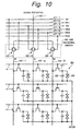
- time-divisional switches 46 having a CMOS, PMOS, or NMOS construction are provided between output lines 45-1, 45-2, 45-3, ... of the driver IC 44 and the signal lines 42-1, 42-2, 42-3, ....
- Fig. 8 shows an example of a connecting construction of the time-divisional switches 46 in case of the 3-time-divisional driving corresponding to R, G, and B.
- signal voltages of three pixels of R, G, and B are time-sequentially outputted through the output lines 45-1, 45-2, 45-3, ... from the output terminals of the driver IC 44.
- signals of pixels R1, G1, and B1 are outputted from an ODD terminal 1 to the output line 45-1 as signal outputs of the driver IC 44; likewise, signals of pixels R2, G2, and B2 are outputted from an EVEN terminal 1 to the output line 45-2; signals of pixels R3, G3, and B3 are outputted from an ODD terminal 2 to the output line 45-3; ....
- every three time-divisional switches are provided for one output line in correspondence to the 3-time-division in a manner such that time-divisional switches 46-1, 46-2, and 46-3 are provided between the output line 45-1 and the three signal lines 42-1, 42-2, and 42-3; time-divisional switches 46-4, 46-5, and 46-6 are provided between the output line 45-2 and the three signal lines 42-4, 42-5, and 42-6; time-divisional switches 46-7, 46-8, and 46-9 are provided between the output line 45-3 and the three signal lines 42-7, 42-8, and 42-9; ....
- the time-divisional switches 46-1, 46-2, and 46-3 comprise CMOS analog switches (transmission switches) in which p-channel MOS transistors and n-channel MOS transistors are connected in parallel and are formed by thin film transistors onto the same substrate as that of the liquid crystal display panel 40. Input terminals of the three time-divisional switches 46-1, 46-2, and 46-3 are connected in common and their common connecting point is connected to the output line 45-1.
- signal potentials which are time-sequentially outputted from the driver IC 44 are inputted to input terminals of the three time-divisional switches 46-1, 46-2, and 46-3 via the output line 45-1.
- Each of output terminals of the time-divisional switches 46-1, 46-2, and 46-3 is connected to one end of each of the three signal lines 42-1, 42-2, and 42-3.
- control lines 47-1 to 47-6 are wired along the wiring directions of the gate lines 41-1, 41-2, 41-3, ....
- Two control input terminals (namely, a gate of an n-channel MOS transistor and a gate of a p-channel MOS transistor) of the time-divisional switch 46-1 are connected to the control lines 47-1 and 47-2.
- Two control input terminals of the time-divisional switch 46-2 are connected to the control lines 47-3 and 47-4 and two control input terminals of the time-divisional switch 46-3 are connected to the control lines 47-5 and 47-6, respectively.
- Control signals S1 to S3 and XS1 to XS3 to select the three time-divisional switches of each set are given from the outside to the six control lines 47-1 to 47-6, respectively.
- the control signals XS1 to XS3 are inversion signals of the control signals S1 to S3.
- the control signals S1 to S3 and XS1 to XS3 are signals for sequentially turning on the three time-divisional switches of each set synchronously with the time-sequential signal potentials which are outputted from the drive IC 44.
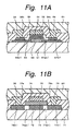
- the time-divisional switches 46-1, 46-2, 46-3, 46-4, 46-5, 46-6, 46-7, 46-8, 46-9, ... of each set are formed in the liquid crystal display panel 40 by the thin film transistors having, for example, a bottom gate structure shown in Fig. 11A or a top gate structure shown in Fig. 11B together with a transistor or the like constructing the vertical driving circuit 43.
- a gate electrode 52 is formed on a glass substrate 51, a polysilicon (Poly-Si) layer 54 is formed on the gate electrode 52 through a gate insulating film 53; and an interlayer insulating film 55 is further formed on the layer 54.
- a source region 56 and a drain region 57 comprising n + type diffusion layers are formed on the gate insulating film 53 on the side of the gate electrode 52.
- the source region 56 and drain region 57 have n - type low impurity concentration portions 56a and 57a, respectively.
- Reference numeral 58 denotes an interlayer insulating film.
- a source electrode 59 and a drain electrode 60 are connected to the n + type source region 56 and drain region 57 through opening portions 58a and 58b formed in the interlayer insulating film 58, respectively.
- Reference numeral 61 denotes an organic film.
- a polysilicon layer 72 is formed on a glass substrate 71.
- a gate electrode 74 is formed on the layer 72 through a gate insulating film 73.
- An interlayer insulating film 75 is further formed on the gate electrode 74.
- a source region 76 and a drain region 77 comprising n + type diffusion layers are formed on the glass substrate 71 on the side of the polysilicon layer 72.
- the source region 76 and drain region 77 have n - type low impurity concentration portions 76a and 77a, respectively.
- a source electrode 78 and a drain electrode 79 are connected to the n + type source region 76 and drain region 77 through connecting holes 75a and 75b formed in the interlayer insulating film 75, respectively.
- Reference numeral 80 denotes an organic film.
- the time-divisional switches 46-1, 46-2, 46-3, 46-4, 46-5, 46-6, 46-7, 46-8, 46-9, ... are sequentially turned on in response to gate selection signals S1, S2, and S3 (refer to the timing chart of Fig. 9) which are supplied from the outside, thereby 3-time-dividing the time-sequential signals which are generated from the driver IC 44 to the output lines 45-1, 45-2, 45-3, ... for one horizontal scanning period, and supplying the time-divided signals to the corresponding signal lines.
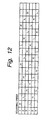
- Fig. 12 shows a writing state of the signal voltage into each pixel in case of the 3-time-divisional driving shown in Fig. 8.
- the lateral direction shows the scanning order and the vertical direction indicates the operating order of the time-divisional switches, respectively.
- H denotes a writing state of a high voltage and L indicates a writing state of a low voltage.
- the number of output pins of the driver IC 44 can be reduced. Specifically speaking, in case of the 3-time-divisional driving, since the number of output pins of the driver IC 44 can be reduced into 1/3 than that in the case where the time-divisional driving is not used, the size in the pin arranging direction of the driver IC can be reduced.
- a compact size can be realized as a liquid crystal display module while stably supplying an excellent picture quality by the dot inversion driving, and the multicolor display can be realized by a cheap liquid crystal display panel.
- the standard of the SHXGA display system is an image display standard of 1024 pixels x 480 pixels and the aspect ratio is set to 32 : 15. This is characterized in that an XGA standard signal can be displayed without laterally scrolling and a VGA (video graphics array) standard signal can be fully displayed.
- the standard of the HXGA display system is an image display standard of 1024 pixels x 384 pixels and the aspect ratio is set to 8 : 3. This is considered to be a portable terminal standard of the XGA standard.
- the total number of signal lines in each system is equal to 3072 and the driver IC 44 to drive the signal lines can be considered in common.
- the miniaturization of the apparatus particularly, the realization of a narrow width of the liquid crystal display panel is actively progressed.
- the size of the frame portion (hereinafter, abbreviated to a frame size) of the liquid crystal display panel it is sufficient to reduce the size of the frame portion (hereinafter, abbreviated to a frame size) of the liquid crystal display panel as small as possible.
- the frame size of 4 mm or less is a target size as an example.
- TAB Transmission Automated Bonding
- a pad size of TAB is equal to about 2 mm at present, in order to satisfy the frame size of 4 mm or less, it is necessary that a size of region which is needed for wiring and connection between the TAB and the time-divisional switches 46-1, 46-2, 46-3, 46-4, 46-5, 46-6, 46-7, 46-8, 46-9, and the like is suppressed to 2 mm or less.
- a wiring width is equal to about 4 ⁇ m and a wiring interval is equal to about 3.5 ⁇ m, a space of about 7.5 ⁇ m is needed per wiring.
- the numerical value of about 266 is derived as the maximum number of lines which can be wired in the frame portion.
- the flexible cables for electrically connecting the output pins of the driver ICs and the time-divisional switches are divided into halves on the right and left sides in the frame portion of the liquid crystal display panel.
- the maximum number of output pins of the driver IC is equal to a value that is twice as large as the maximum number of lines (266) which can be wired, namely, about 532.
- the driver IC It also contributes to the reduction of costs of the driver IC. Moreover, in future, the more number of pins of the driver IC is expected in association with the progress of the integrated circuit technique and the number of driver ICs can be set to 3 or less in accordance with it, so that the further reduction of the electric power consumption and the product costs can be expected.
- the horizontal scanning time of the SXGA display system is determined to 21.537 ⁇ sec, 15.63 ⁇ sec, 12.504 ⁇ sec, and 10.971 ⁇ sec on the standard. To realize the constructions of Figs. 10 and 14 under the above standard, for example, it is necessary to match with 10.971 ⁇ sec as the shortest horizontal scanning time.
- the 3-time-division is now performed, it is necessary to select time that is equal to or shorter than 1/3 of 10.971 ⁇ sec. That is, it is necessary that the sampling time is equal to 3.657 ⁇ sec or less. Similarly, if the horizontal scanning time is equal to 21.537 ⁇ sec, the sampling time is equal to 7.179 ⁇ sec or less; if it is equal to 15.63 ⁇ sec, the sampling time is equal to 5.21 ⁇ sec or less; and if it is equal to 12.504 ⁇ sec, the sampling time is equal to 4.168 ⁇ sec or less.
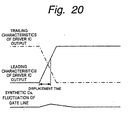
- leading and trailing times (throughrate) of output waveforms which are outputted from the driver IC 44 to the signal lines since it is necessary to finish them within the sampling time, it is necessary to set to a period shorter than a selecting period of time. It is defined that the leading and trailing times of the driver IC 44 are set to the time which varies within a range of 0% ⁇ 99.75%. For example, when a signal amplitude of the signal line is equal to 9V, there is an error of 0.00225V.
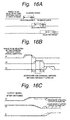
- the time-divisional switch of R After the time-divisional switch of R was selected, it is necessary to provide a blanking period for a period of time until the second time-divisional switch is selected. This is because the signal potential of the non-selection signal line in which the electric potential has been determined fluctuates.
- the selection signal line connected to the time-divisional switch increases in size, a parasitic capacitance or a wiring resistance certainly exists and a delay occurs in the selection line time due to it. Thus, since the adjacent time-divisional switches are simultaneously turned on/off, the signal potential of the non-selection signal line cannot be decided.
- Fig. 16A shows a period which is selected by the time-divisional switches at the input terminal
- Fig. 16B shows a period which is selected by the time-divisional switches in the liquid crystal substrate
- Fig. 16C shows a signal output after the time-divisional switches, respectively.
- a solid line indicates a case where the blanking period is provided.
- a broken line shows a case where the blanking period is not provided.
- the adjacent gate lines are simultaneously turned on/off, thereby causing a fluctuation of the pixel potential.
- the blanking period is also necessary in the switching period of time of the gate selecting pulse. Therefore, if the time of (scanning time in the horizontal direction - selecting time x 3)/3 is insufficient as a blanking period (c), the time longer than that is necessary. In the driving circuit of the existing selective switch, 40 nsec is necessary as a short blanking period and is the minimum value.
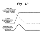
- jitters of the gate lines 41-1, 41-2, 41-3, ... and periodic fluctuations of Cs lines 48-1, 48-2, 48-3, ... are induced as shown in a waveform diagram of Fig. 18 by a diving potential from the signal lines 42-1, 42-2, 42-3, 42-4, ... which are caused due to a parasitic capacitance Cgs between the gate lines 41-1, 41-2, 41-3, ... and the signal lines (source lines) 42-1, 42-2, 42-3, 42-4, ... and a parasitic capacitance Ccs between the Cs lines 48-1, 48-2, 48-3, ... to supply the common voltage VCOM to the counter electrodes of the pixels and the signal lines 42-1, 42-2, 42-3, 42-4, ....
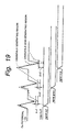
- fluctuating potentials of the jitters of the Cs lines 48-1, 48-2, 48-3, ... are specified by ⁇ s1, ⁇ s2, and ⁇ s3 shown in Fig. 19.
- ⁇ s1, ⁇ s2, and ⁇ s3 denote potential differences between a crosstalk generating region and a non-generating region. It has been found that if the potential differences ⁇ s1, ⁇ s2, and ⁇ s3 are equal to or less than 70 mV, they are not judged as an image. That is, at present, if such a condition is satisfied, they are not decided as a crosstalk in the lateral direction.
- the dot inversion driving system in which the polarities between the adjacent pixels are inverted while the counter electrode is used as a reference is used.
- the leading time and the trailing time become the times which cannot be ignored as compared with those in the conventional liquid crystal display in which the signal lines 42-1, 42-2, 42-3, ... are connected to the output pins of the driver IC 44 in a one-to-one correspondence relationship.
- the time necessary to settle the Cs lines 48-1, 48-2, 48-3, ... is equal to 1/3 of the conventional one and the conditions become severe.
- the fluctuating potential amount can be cancelled by the signals of the opposite polarities, so that most of the fluctuations of the gate lines 41-1, 41-2, 41-3, ... and Cs lines 48-1, 48-2, 48-3, ... are eliminated.
- the fluctuation amount is smaller, the time that is required to settle the electric potentials of the Cs lines 48-1, 48-2, 48-3, ... becomes shorter.
- Fig. 21 shows a simulation result in case of the SXGA display system of 17 inches as an example.
- 3 ⁇ rise - 3 ⁇ fall ⁇ 500 nsec or 2 ⁇ rise - 2 ⁇ fall ⁇ 500 nsec where, ⁇ is constant at 0.5 ⁇ sec, 3 ⁇ indicates a transition from 0% to 90%, and 2 ⁇ indicates a transition from 0% to 86%, respectively.
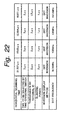
- Fig. 22 shows an example of numerical values of the periods in case of manufacturing the liquid crystal display of the SXGA display system.
- driver IC It also contributes to the reduction of the costs of the driver IC. Moreover, in future, in association with the progress of the integrated circuit technique, the more number of pins of the driver IC is expected and four or less driver ICs can be also set in accordance with it. Thus, the further reduction of the electric power consumption and the product costs can be expected.
- the horizontal scanning times of the UXGA display system are determined to 16 ⁇ sec, 13.333 ⁇ sec, 12.308 ⁇ sec, 11.429 ⁇ sec, 10.667 ⁇ sec, 10 ⁇ sec, and 9.412 ⁇ sec on the standard.
- the sampling time is equal to 5.333 ⁇ sec or less; if it is equal to 13.333 ⁇ sec, the sampling time is equal to 4.444 ⁇ sec or less; if it is equal to 12.308 ⁇ sec, the sampling time is equal to 4.103 ⁇ sec or less; if it is equal to 11.429 ⁇ sec, the sampling time is equal to 3.810 ⁇ sec or less; if it is equal to 10 ⁇ sec, the sampling time is equal to 3.333 ⁇ sec or less.
- Fig. 24 shows an example of numerical values of the period of time in case of manufacturing the liquid crystal display of the UXGA display system.
- the number of output pins of the driver IC is set to 320 under conditions similar to those in the case of each display system of SXGA and UXGA mentioned above.
- the two driver ICs 44-1 and 44-2 each having 320 output pins are arranged at a predetermined interval on an external substrate (not shown) different from the liquid crystal display panel 40 and connected to the time-divisional switches (not shown) in the connecting portions 16 of the frame of the liquid crystal display panel 40 through the flexible cables 15.
- the 3-time-divisional driving in the liquid crystal display of the VGA display system for example, when the number of output pins of the driver IC is set to 320, it is sufficient to use two driver ICs.
- driver IC It also contributes to the reduction of the costs of the driver IC. Moreover, in future, in association with the progress of the integrated circuit technique, the more number of pins of the driver IC is expected and one driver IC can be also set in accordance with it. Thus, the further reduction of the electric power consumption and the product costs can be expected.
- the standard of the HVGA display system is a standard of 640 pixels x 240 pixels and the number of pixels in the horizontal direction is the same as that of the VGA display system, so that the total number of signal lines is also equal to 1920. Therefore, if the number of output pins of the driver IC is set to, for example, 320, the number of driver ICs which are set is also equal to 2.
- the standard of the QVGA display system is a standard of 320 pixels x 240 pixels and the total number of signal lines is equal to 960.
- the number of output pins of the driver IC is set to, for example, 320
- it is sufficient to set the total output pins of the driver IC to 1/3 of the number of signal lines (960 lines). Therefore, in the QVGA display system, as shown in Fig. 26, the number of driver ICs is set to 1 ( 320/320).
- the horizontal scanning time is equal to 31.778 ⁇ sec. Since the 3-time-division is performed, it is necessary to select the time that is equal to or less than 1/3 of 31.778 ⁇ sec. That is, it is necessary to set the sampling time to 10.59 ⁇ sec or less. In the QVGA display system, for example, now assuming that the horizontal scanning time is set to 63 ⁇ sec, it is necessary to set the sampling time to 10.59 ⁇ sec or less in the 3-time-division.
- Fig. 27 shows an example of numerical values of the period of time in case of manufacturing the liquid crystal display of each display system of VGA and QVGA.
- the time-divisional switches are OFF and the electric potentials of the signal lines have been determined. Therefore, they are not influenced by an output from the driver IC as an external IC. Thus, when the output circuit of the driver IC is driven in the blanking periods (a), (b), and (C), the electric power is consumed in vain.
- Fig. 4 shows an example of an internal construction of the driver IC.
- an output circuit 36 is usually arranged at the post stage of the D/A converter 35. It is, therefore, assumed that the output circuit 36 is made inoperative for the blanking periods (a), (b), and (c), thereby reducing the electric power consumption.
- the output circuit 36 has a circuit construction of, for instance, a voltage follower comprising an operational amplifier and an output buffer.
- the output circuit 36 of the voltage follower circuit construction for example, when a power source of the voltage follower is turned off for the blanking periods (a), (b), and (c), no current flows in the operational amplifier portion and an output enters a high impedance state. As mentioned above, by making the output circuit 36 inoperative for the blanking periods (a), (b), and (c), the electric power consumption can be reduced.
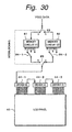
- two memory circuits (1) 81 and (2) 82 each having a storage capacity corresponding to one line are connected to the liquid crystal display panel 40 through, for example, three driver ICs 44-1, 44-2, and 44-3.
- the memory circuits 81 and 82 are switched and a procedure similar to that mentioned above is repeated, thereby constructing an image.
- the data is sent like beads and the data of one line is set into a plurality of driver ICs.
- the data of one line is set into the liquid crystal display panel 40 in a lump.
- the number of pixels in the horizontal direction also increases and, at the same time, a transfer rate of video data also rises and the writing time to the liquid crystal display panel also becomes short.
- the data transfer rate of the video data is equal to about 200 MHz and the driver IC which can write the data at this speed does not exist at present.
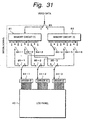
- Fig. 31 shows an example of a specific construction to realize it. In the example, to easily explain, explanation will be made on the assumption that the number of horizontal pixels is set to 30 (total 90 dots for R, G, and B) and the number of shift registers 31 (refer to Fig. 28) in each driver IC is set to 10, respectively.
- two memory circuits (1) 81 and (2) 82 each having a storage capacity corresponding to one line are provided.
- the video data is supplied to the memory circuit 81 or 82 via the switch 83 to switch those memory circuits.
- Switches 84-1 to 84-6 for switching the colors of R, G, and B are provided on the output sides of the memory circuits 81 and 82 in a manner such that one switch is provided for every three terminals.
- Switches 85-1 to 85-3 each for switching again the memory circuits 81 and 82 are further provided at the post stage of the switches 84-1 to 84-6. Selection outputs of the switches 85-1 to 85-3 are supplied to the driver ICs 44-1 to 44-3, respectively.
- the switch 83 since the switch 83 has initially been switched to the memory circuit 81 side, the video data which is inputted from the outside is stored into the memory circuit 81 through the switch 83 by an amount of one line. After that, since the switch 83 is switched to the memory circuit 82 side, the video data of next one line is stored into the memory circuit 82.
- the memory circuit 81 outputs the data of the first to the 10th dots to the driver IC 44-1, outputs the data of the 11th to the 20th dots to the driver IC 44-2, and outputs the data of the 21st to the 30th dots to the driver IC 44-3, respectively.
- the memory circuits 81 and 82 are switched and the operation similar to that mentioned above is performed and repeated, so that one image is constructed.
- the data of one line is first stored into the memory circuit 81 and while the data is stored into the memory circuit 82 for the next 1-line period, only R is selected by the switches 84-1 to 84-3, the R data as much as one driver IC is read out from the memory circuit 81 and written into the relevant driver IC. At the same time, the relevant data is also read out and written into another driver IC. By also writing the relevant data by a similar method with respect to G and B, the different data can be simultaneously written into each of the driver ICs.
- the speed at which the data is written into each driver IC can be reduced into 1/n. Therefore, for example, if the transfer rate of the video data is equal to 200 MHz and the number n of driver ICs is equal to 3, the data can be processed by the driver IC having an operating speed of about 67 MHz and it is possible to sufficiently cope with such a situation by the existing driver ICs. Since the writing time that is required to write all of the data of one line into each driver IC can be reduced into 1/n, the writing time to the liquid crystal display panel can be extended by only the time corresponding to such a reduced writing time.
- Figs. 32A and 32B show characteristics curves (V-T curves) of the transmittance of the liquid crystal and the voltage to be applied to the liquid crystal in case of using a TN (twist nematic) liquid crystal.
- V-T curves characteristics curves
- the V-T curve is shifted in R (transmission wavelength is 600 to 660 nm), G (transmission wavelength is 530 to 550 nm), and B (transmission wavelength is 370 to 460 nm).
- the signal lines other than the selected switches are in a floating state. In this state, the signal lines are influenced by the diving of the signal potential between the adjacent signal lines. That is, an interline capacitance exists between the signal lines of the pixel.
- Figs. 33A, 33B, and 33C showing equivalent circuits around the time-divisional switches for example, when the switch S2 is selected (Fig. 33B) after the switch S1 was selected (Fig. 33A), the signal at the "H" level of the switch S2 dives into the switch S1 and the held voltage is increased by only an amount of the diving capacitance.
- Vsig denotes an amplitude voltage of the signal voltage which is inputted to the selected signal line. It is sufficient to decide a value of the amplitude voltage so as to just complement a shift amount of the applied voltage in a state of the same transmittance of halftone on the V-T curve of the liquid crystal.
- a shift amount of the voltages of R and B is equal to 0.3V and is allocated to the voltage ⁇ V due to the diving.
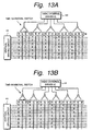
- the 1HVCOM (common) inversion driving method since the voltage of the same polarity is applied to the signal line for a 1H time, with respect to the switch S1 which has previously been selected, the held electric potential of the signal line increases when the next switch S2 is selected.
- the switch S3 is subsequently selected (Fig. 33C). This means that the diving potential is inputted from a switch S3' adjacent to the switch S1. Finally, the signal lines are influenced by the diving potential between the signal lines twice with respect to the switch S1 and once with regard to the switch S2.
- the signal lines are arranged in a manner such that the signal line which is selected at first is set to B, the signal line which is selected at the second time is set to G, and the signal line which is selected at the third time is set to R, thereby performing the complementing of the V-T curve mentioned before.
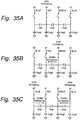
- the diving voltage is generated in a decreasing direction. That is, as shown in Figs. 35A, 35B, and 35C, when the signal is written at the "H" level into the switch S1 (Fig. 35A) and, thereafter, when the signal is written at the "L” level into the switch S2 (Fig. 35B), the electric potential at the "L” level dives into the non-selected switch S1. After that, the signal at the "H” level is written into the switch S3 (Fig. 35C). However, a diving potential at the "H” level similarly occurs for a switch S1' adjacent to the switch S3.
- the switch S3' adjacent to the switch S1 is set to the "L" level because of the dot inversion driving. This "L" level signal dives into the switch S1 and the voltage further decreases. Finally, the voltage to reduce the signal voltage occurs twice for the switch S1 selected first. The voltage to reduce the signal voltage occurs once for the switch S2.
- Fig. 37A and 37B show relations between the pixel array and the scanning direction of the time-divisional switches according to the invention.
- Fig. 37A shows the case of the 1H inversion driving method
- Fig. 37B shows the case of the dot inversion driving method, respectively.
- the above method can present an extremely large effect from a viewpoint that since the capacitance existing between the signal lines is actively used for complementing the voltage-transmittance characteristics of the liquid crystal, a complicated circuit construction is not needed, and the invention can be accomplished by setting only the color array to a predetermined order.
- the number of output terminals of each of a plurality of driver circuits is set to the measure of the total number of signal lines as many as a plurality of columns, no fraction occurs in the signal lines and the output terminals of the driver circuits can be connected to the signal lines without causing a remainder in the output terminals. Therefore, a surplus connecting region which does not contribute to the image display is not caused on the liquid crystal display panel, so that the width in the horizontal direction of the liquid crystal display panel can be narrowed.
Landscapes
- Engineering & Computer Science (AREA)
- Physics & Mathematics (AREA)
- General Physics & Mathematics (AREA)
- Theoretical Computer Science (AREA)
- Computer Hardware Design (AREA)
- Crystallography & Structural Chemistry (AREA)
- Chemical & Material Sciences (AREA)
- Nonlinear Science (AREA)
- Liquid Crystal (AREA)
- Mathematical Physics (AREA)
- Optics & Photonics (AREA)
- Liquid Crystal Display Device Control (AREA)
- Control Of Indicators Other Than Cathode Ray Tubes (AREA)
Applications Claiming Priority (3)
| Application Number | Priority Date | Filing Date | Title |
|---|---|---|---|
| JP7681398 | 1998-03-25 | ||
| JP24139298A JP4232227B2 (ja) | 1998-03-25 | 1998-08-27 | 表示装置 |
| EP99909300A EP1069457A4 (de) | 1998-03-25 | 1999-03-23 | Flüssigkristallanzeigevorrichtung |
Related Parent Applications (1)
| Application Number | Title | Priority Date | Filing Date |
|---|---|---|---|
| EP99909300A Division EP1069457A4 (de) | 1998-03-25 | 1999-03-23 | Flüssigkristallanzeigevorrichtung |
Publications (2)
| Publication Number | Publication Date |
|---|---|
| EP1755105A2 true EP1755105A2 (de) | 2007-02-21 |
| EP1755105A3 EP1755105A3 (de) | 2007-06-20 |
Family
ID=26417935
Family Applications (2)
| Application Number | Title | Priority Date | Filing Date |
|---|---|---|---|
| EP99909300A Withdrawn EP1069457A4 (de) | 1998-03-25 | 1999-03-23 | Flüssigkristallanzeigevorrichtung |
| EP06125738A Withdrawn EP1755105A3 (de) | 1998-03-25 | 1999-03-23 | Steuerschaltung für Farbflüssigkeitskristallanzeiger |
Family Applications Before (1)
| Application Number | Title | Priority Date | Filing Date |
|---|---|---|---|
| EP99909300A Withdrawn EP1069457A4 (de) | 1998-03-25 | 1999-03-23 | Flüssigkristallanzeigevorrichtung |
Country Status (4)
| Country | Link |
|---|---|
| EP (2) | EP1069457A4 (de) |
| JP (2) | JP4232227B2 (de) |
| KR (2) | KR100702635B1 (de) |
| WO (1) | WO1999049355A1 (de) |
Cited By (1)
| Publication number | Priority date | Publication date | Assignee | Title |
|---|---|---|---|---|
| WO2012161701A1 (en) * | 2011-05-24 | 2012-11-29 | Apple Inc. | Application of voltage to data lines during vcom toggling |
Families Citing this family (41)
| Publication number | Priority date | Publication date | Assignee | Title |
|---|---|---|---|---|
| JP2001325798A (ja) * | 2000-05-16 | 2001-11-22 | Sony Corp | 論理回路およびこれを用いた表示装置 |
| JP2002099260A (ja) * | 2000-09-26 | 2002-04-05 | Toshiba Corp | 信号線駆動回路 |
| JP4923343B2 (ja) * | 2001-07-12 | 2012-04-25 | ソニー株式会社 | 表示装置およびこれを搭載した携帯端末 |
| JP2003107513A (ja) | 2001-09-27 | 2003-04-09 | Citizen Watch Co Ltd | 液晶表示装置 |
| EP1300826A3 (de) | 2001-10-03 | 2009-11-18 | Nec Corporation | Anzeigegerät und Halbleiteranordnung |
| JP4409152B2 (ja) | 2002-06-27 | 2010-02-03 | 株式会社ルネサステクノロジ | 表示制御駆動装置および表示システム |
| JP3685176B2 (ja) | 2002-11-21 | 2005-08-17 | セイコーエプソン株式会社 | 駆動回路、電気光学装置及び駆動方法 |
| KR100927021B1 (ko) * | 2003-02-28 | 2009-11-16 | 엘지디스플레이 주식회사 | 액정표시패널의 구동방법 및 장치 |
| JP4363881B2 (ja) * | 2003-04-10 | 2009-11-11 | 東芝モバイルディスプレイ株式会社 | 液晶表示装置 |
| JP2004341251A (ja) * | 2003-05-15 | 2004-12-02 | Renesas Technology Corp | 表示制御回路及び表示駆動回路 |
| JP4144474B2 (ja) * | 2003-08-22 | 2008-09-03 | ソニー株式会社 | 画像表示装置、画像表示パネル、パネル駆動装置および画像表示パネルの駆動方法 |
| JP4176688B2 (ja) | 2003-09-17 | 2008-11-05 | シャープ株式会社 | 表示装置およびその駆動方法 |
| JP3875229B2 (ja) | 2003-11-13 | 2007-01-31 | シャープ株式会社 | データラインの駆動方法およびそれを用いた表示装置並びに液晶表示装置 |
| KR100598741B1 (ko) | 2003-12-11 | 2006-07-10 | 엘지.필립스 엘시디 주식회사 | 액정표시장치 |
| US7586474B2 (en) * | 2003-12-11 | 2009-09-08 | Lg Display Co., Ltd. | Liquid crystal display and method of driving the same |
| US7492343B2 (en) * | 2003-12-11 | 2009-02-17 | Lg Display Co., Ltd. | Liquid crystal display device |
| JP2005181777A (ja) * | 2003-12-22 | 2005-07-07 | Sony Corp | 表示装置及びその駆動方法 |
| JP2005234057A (ja) | 2004-02-17 | 2005-09-02 | Sharp Corp | 画像表示装置 |
| JP4511218B2 (ja) * | 2004-03-03 | 2010-07-28 | ルネサスエレクトロニクス株式会社 | ディスプレイパネル駆動方法,ドライバ,及びディスプレイパネル駆動用プログラム |
| JP4694134B2 (ja) * | 2004-03-09 | 2011-06-08 | 株式会社 日立ディスプレイズ | 表示装置 |
| JP2005321745A (ja) * | 2004-04-07 | 2005-11-17 | Sony Corp | 表示装置および表示装置の駆動方法 |
| JP2005300885A (ja) * | 2004-04-12 | 2005-10-27 | Koninkl Philips Electronics Nv | 液晶表示装置 |
| JP2005331709A (ja) * | 2004-05-20 | 2005-12-02 | Renesas Technology Corp | 液晶表示駆動装置および液晶表示システム |
| JP4152420B2 (ja) | 2004-07-21 | 2008-09-17 | シャープ株式会社 | アクティブマトリクス型表示装置およびそれに用いられる駆動制御回路 |
| KR100640894B1 (ko) * | 2004-09-07 | 2006-11-02 | 엘지전자 주식회사 | 이동통신 단말기용 컬러 액정 표시 장치의 제어 장치 및 제어방법 |
| JP2006154545A (ja) * | 2004-11-30 | 2006-06-15 | Sanyo Electric Co Ltd | 液晶表示装置 |
| JP4710422B2 (ja) * | 2005-06-03 | 2011-06-29 | カシオ計算機株式会社 | 表示駆動装置及び表示装置 |
| US7576724B2 (en) | 2005-08-08 | 2009-08-18 | Tpo Displays Corp. | Liquid crystal display device and electronic device |
| US7633495B2 (en) * | 2006-02-14 | 2009-12-15 | Tpo Displays Corp. | Driving circuit with low power consumption multiplexer and a display panel and an electronic device using the same |
| KR100784014B1 (ko) * | 2006-04-17 | 2007-12-07 | 삼성에스디아이 주식회사 | 유기전계발광 표시장치 및 그의 구동방법 |
| KR101329423B1 (ko) * | 2007-04-23 | 2013-11-14 | 엘지디스플레이 주식회사 | 액정 표시 장치 및 이의 구동 방법 |
| US8319760B2 (en) | 2007-06-29 | 2012-11-27 | Sony Corporation | Display device, driving method of the same and electronic equipment incorporating the same |
| JP4427763B2 (ja) | 2007-12-10 | 2010-03-10 | ソニー株式会社 | ディスプレイ |
| JP4845154B2 (ja) * | 2009-04-02 | 2011-12-28 | ルネサスエレクトロニクス株式会社 | 液晶表示駆動装置および表示システム |
| EP2474964B1 (de) | 2009-09-02 | 2014-04-16 | Sharp Kabushiki Kaisha | Substrat einer anzeigevorrichtung |
| JP5413474B2 (ja) * | 2012-03-09 | 2014-02-12 | セイコーエプソン株式会社 | 電気光学装置、電子機器および電気光学装置の駆動方法。 |
| KR102098717B1 (ko) * | 2013-08-22 | 2020-04-09 | 삼성디스플레이 주식회사 | 표시 장치 |
| JP6357765B2 (ja) * | 2013-12-10 | 2018-07-18 | セイコーエプソン株式会社 | 駆動装置、電気光学装置及び電子機器 |
| JP6354355B2 (ja) * | 2014-06-09 | 2018-07-11 | セイコーエプソン株式会社 | 電気光学装置、電子機器、及び電気光学装置の制御方法 |
| CN104777687B (zh) * | 2015-04-29 | 2017-12-26 | 深圳市华星光电技术有限公司 | 阵列基板及具有该阵列基板的显示装置 |
| JP7329565B2 (ja) * | 2021-07-20 | 2023-08-18 | シャープディスプレイテクノロジー株式会社 | 液晶表示装置 |
Citations (2)
| Publication number | Priority date | Publication date | Assignee | Title |
|---|---|---|---|---|
| US5426447A (en) | 1992-11-04 | 1995-06-20 | Yuen Foong Yu H.K. Co., Ltd. | Data driving circuit for LCD display |
| US5440304A (en) * | 1992-07-27 | 1995-08-08 | Rohm Co., Ltd. | Integrated circuit having a shift stage count changing function |
Family Cites Families (15)
| Publication number | Priority date | Publication date | Assignee | Title |
|---|---|---|---|---|
| JPH0824359B2 (ja) * | 1986-03-03 | 1996-03-06 | 株式会社日立製作所 | アクティブマトリクス型画像表示装置 |
| EP0275140B1 (de) * | 1987-01-09 | 1995-07-19 | Hitachi, Ltd. | Verfahren und Schaltung zum Abtasten von kapazitiven Belastungen |
| JPH0778672B2 (ja) * | 1987-09-28 | 1995-08-23 | 松下電器産業株式会社 | 半導体素子 |
| JPS6484297A (en) * | 1987-09-28 | 1989-03-29 | Toshiba Corp | Display device |
| JPH01118895A (ja) * | 1987-10-31 | 1989-05-11 | Fujitsu General Ltd | 液晶ディスプレイパネルの駆動方法 |
| JP2581796B2 (ja) * | 1988-04-25 | 1997-02-12 | 株式会社日立製作所 | 表示装置及び液晶表示装置 |
| JP2840378B2 (ja) * | 1990-04-28 | 1998-12-24 | 三洋電機株式会社 | 液晶表示装置 |
| JPH0452684A (ja) * | 1990-06-20 | 1992-02-20 | Nec Kansai Ltd | 液晶表示パネルの駆動方法 |
| JP2509017B2 (ja) * | 1991-07-24 | 1996-06-19 | 富士通株式会社 | アクティブマトリクス型液晶表示装置 |
| GB9207527D0 (en) * | 1992-04-07 | 1992-05-20 | Philips Electronics Uk Ltd | Multi-standard video matrix display apparatus and its method of operation |
| JP3219640B2 (ja) * | 1994-06-06 | 2001-10-15 | キヤノン株式会社 | ディスプレイ装置 |
| EP0760508B1 (de) * | 1995-02-01 | 2005-11-09 | Seiko Epson Corporation | Verfahren und einrichtung zum steuern einer flüssigkristallanzeige |
| JP3110980B2 (ja) * | 1995-07-18 | 2000-11-20 | インターナショナル・ビジネス・マシーンズ・コーポレ−ション | 液晶表示装置の駆動装置及び方法 |
| US5838060A (en) * | 1995-12-12 | 1998-11-17 | Comer; Alan E. | Stacked assemblies of semiconductor packages containing programmable interconnect |
| JP3277121B2 (ja) * | 1996-05-22 | 2002-04-22 | インターナショナル・ビジネス・マシーンズ・コーポレーション | 液晶デイスプレイの中間表示駆動方式 |
-
1998
- 1998-08-27 JP JP24139298A patent/JP4232227B2/ja not_active Expired - Fee Related
-
1999
- 1999-03-23 WO PCT/JP1999/001441 patent/WO1999049355A1/ja not_active Ceased
- 1999-03-23 EP EP99909300A patent/EP1069457A4/de not_active Withdrawn
- 1999-03-23 KR KR1019997012190A patent/KR100702635B1/ko not_active Expired - Fee Related
- 1999-03-23 KR KR1020067000168A patent/KR100635445B1/ko not_active Expired - Fee Related
- 1999-03-23 EP EP06125738A patent/EP1755105A3/de not_active Withdrawn
-
2008
- 2008-09-16 JP JP2008236441A patent/JP4835667B2/ja not_active Expired - Lifetime
Patent Citations (2)
| Publication number | Priority date | Publication date | Assignee | Title |
|---|---|---|---|---|
| US5440304A (en) * | 1992-07-27 | 1995-08-08 | Rohm Co., Ltd. | Integrated circuit having a shift stage count changing function |
| US5426447A (en) | 1992-11-04 | 1995-06-20 | Yuen Foong Yu H.K. Co., Ltd. | Data driving circuit for LCD display |
Cited By (2)
| Publication number | Priority date | Publication date | Assignee | Title |
|---|---|---|---|---|
| WO2012161701A1 (en) * | 2011-05-24 | 2012-11-29 | Apple Inc. | Application of voltage to data lines during vcom toggling |
| US8593491B2 (en) | 2011-05-24 | 2013-11-26 | Apple Inc. | Application of voltage to data lines during Vcom toggling |
Also Published As
| Publication number | Publication date |
|---|---|
| JP2009009156A (ja) | 2009-01-15 |
| KR100635445B1 (ko) | 2006-10-18 |
| EP1069457A1 (de) | 2001-01-17 |
| WO1999049355A1 (en) | 1999-09-30 |
| JPH11338438A (ja) | 1999-12-10 |
| KR100702635B1 (ko) | 2007-04-02 |
| EP1755105A3 (de) | 2007-06-20 |
| KR20010014131A (ko) | 2001-02-26 |
| JP4835667B2 (ja) | 2011-12-14 |
| KR20060011918A (ko) | 2006-02-03 |
| JP4232227B2 (ja) | 2009-03-04 |
| EP1069457A4 (de) | 2006-01-25 |
Similar Documents
| Publication | Publication Date | Title |
|---|---|---|
| EP1755105A2 (de) | Steuerschaltung für Farbflüssigkeitskristallanzeiger | |
| US7903072B2 (en) | Electro-optical device, driving circuit, and electronic apparatus for decreasing frame size | |
| US5739802A (en) | Staged active matrix liquid crystal display with separated backplane conductors and method of using the same | |
| KR100371841B1 (ko) | 전기 광학 장치의 구동 방법, 전기 광학 장치의 구동회로, 전기 광학 장치 및 전자기기 | |
| KR100757766B1 (ko) | 표시 장치 및 주사선용 드라이버 회로 | |
| US8035634B2 (en) | Electro-optical device, driving circuit, and electronic apparatus | |
| US20030132903A1 (en) | Liquid crystal display device having an improved precharge circuit and method of driving same | |
| US6011530A (en) | Liquid crystal display | |
| JP2010102189A (ja) | 液晶表示装置及びその駆動方法 | |
| KR100549983B1 (ko) | 액정표시장치 및 그 구동방법 | |
| JP2001042287A (ja) | 液晶表示装置およびその駆動方法 | |
| US7508371B2 (en) | Liquid crystal display device | |
| US6795050B1 (en) | Liquid crystal display device | |
| US20160232862A1 (en) | Display apparatus | |
| US6911962B1 (en) | Driving method of active matrix display device | |
| KR20060080778A (ko) | 표시장치의 구동방법 및 이를 수행하기 위한 표시장치 | |
| US8284146B2 (en) | Display device, its driving circuit, and driving method | |
| JP4720261B2 (ja) | 電気光学装置、駆動方法および電子機器 | |
| JP2007279539A (ja) | ドライバ回路、表示装置及びその駆動方法 | |
| JP2000275611A (ja) | 液晶表示装置 | |
| US20120162161A1 (en) | Liquid crystal display | |
| JPH11161237A (ja) | 液晶表示装置 | |
| US7675499B2 (en) | Display device | |
| US7948458B2 (en) | Amplifier circuit and display device | |
| KR100412120B1 (ko) | 액정표시장치의 구동회로 및 그 구동방법 |
Legal Events
| Date | Code | Title | Description |
|---|---|---|---|
| PUAI | Public reference made under article 153(3) epc to a published international application that has entered the european phase |
Free format text: ORIGINAL CODE: 0009012 |
|
| AC | Divisional application: reference to earlier application |
Ref document number: 1069457 Country of ref document: EP Kind code of ref document: P |
|
| AK | Designated contracting states |
Kind code of ref document: A2 Designated state(s): DE GB NL |
|
| PUAL | Search report despatched |
Free format text: ORIGINAL CODE: 0009013 |
|
| AK | Designated contracting states |
Kind code of ref document: A3 Designated state(s): DE GB NL |
|
| 17P | Request for examination filed |
Effective date: 20071211 |
|
| 17Q | First examination report despatched |
Effective date: 20080115 |
|
| AKX | Designation fees paid |
Designated state(s): DE GB NL |
|
| RAP1 | Party data changed (applicant data changed or rights of an application transferred) |
Owner name: JAPAN DISPLAY WEST INC. |
|
| STAA | Information on the status of an ep patent application or granted ep patent |
Free format text: STATUS: THE APPLICATION IS DEEMED TO BE WITHDRAWN |
|
| 18D | Application deemed to be withdrawn |
Effective date: 20160405 |