EP1755233A2 - Blocs de commande pouvant être parametrés par logiciel utilisés dans le traitement de couche physique - Google Patents
Blocs de commande pouvant être parametrés par logiciel utilisés dans le traitement de couche physique Download PDFInfo
- Publication number
- EP1755233A2 EP1755233A2 EP06122605A EP06122605A EP1755233A2 EP 1755233 A2 EP1755233 A2 EP 1755233A2 EP 06122605 A EP06122605 A EP 06122605A EP 06122605 A EP06122605 A EP 06122605A EP 1755233 A2 EP1755233 A2 EP 1755233A2
- Authority
- EP
- European Patent Office
- Prior art keywords
- processor
- tdd
- fdd
- transmit
- channel
- Prior art date
- Legal status (The legal status is an assumption and is not a legal conclusion. Google has not performed a legal analysis and makes no representation as to the accuracy of the status listed.)
- Withdrawn
Links
- 238000012545 processing Methods 0.000 title claims abstract description 126
- 239000002131 composite material Substances 0.000 claims abstract description 82
- 238000000034 method Methods 0.000 claims abstract description 28
- 238000004891 communication Methods 0.000 claims abstract description 10
- 230000015654 memory Effects 0.000 claims description 82
- 230000011218 segmentation Effects 0.000 claims description 29
- 238000012546 transfer Methods 0.000 claims description 20
- 230000005540 biological transmission Effects 0.000 claims description 18
- 238000013507 mapping Methods 0.000 claims description 10
- 238000012937 correction Methods 0.000 claims description 7
- 238000003780 insertion Methods 0.000 claims description 7
- 230000037431 insertion Effects 0.000 claims description 7
- 230000007480 spreading Effects 0.000 claims description 7
- 238000001914 filtration Methods 0.000 claims description 6
- 240000007320 Pinus strobus Species 0.000 claims 3
- 230000008878 coupling Effects 0.000 claims 1
- 238000010168 coupling process Methods 0.000 claims 1
- 238000005859 coupling reaction Methods 0.000 claims 1
- 230000008569 process Effects 0.000 abstract description 21
- 230000006870 function Effects 0.000 description 13
- 238000013459 approach Methods 0.000 description 10
- 238000010586 diagram Methods 0.000 description 10
- 230000008859 change Effects 0.000 description 3
- 238000013461 design Methods 0.000 description 3
- 206010009944 Colon cancer Diseases 0.000 description 2
- 238000001514 detection method Methods 0.000 description 2
- 235000019800 disodium phosphate Nutrition 0.000 description 2
- 230000000694 effects Effects 0.000 description 2
- 239000000284 extract Substances 0.000 description 2
- 239000000945 filler Substances 0.000 description 2
- 239000011159 matrix material Substances 0.000 description 2
- 238000012163 sequencing technique Methods 0.000 description 2
- 230000003139 buffering effect Effects 0.000 description 1
- 230000001934 delay Effects 0.000 description 1
- 230000009977 dual effect Effects 0.000 description 1
- 230000008570 general process Effects 0.000 description 1
- 239000003550 marker Substances 0.000 description 1
- 230000007246 mechanism Effects 0.000 description 1
- 230000009467 reduction Effects 0.000 description 1
- 230000001360 synchronised effect Effects 0.000 description 1
- 230000009897 systematic effect Effects 0.000 description 1
- 208000037918 transfusion-transmitted disease Diseases 0.000 description 1
Images




Classifications
-
- H—ELECTRICITY
- H04—ELECTRIC COMMUNICATION TECHNIQUE
- H04W—WIRELESS COMMUNICATION NETWORKS
- H04W88/00—Devices specially adapted for wireless communication networks, e.g. terminals, base stations or access point devices
- H04W88/02—Terminal devices
- H04W88/06—Terminal devices adapted for operation in multiple networks or having at least two operational modes, e.g. multi-mode terminals
-
- H—ELECTRICITY
- H04—ELECTRIC COMMUNICATION TECHNIQUE
- H04W—WIRELESS COMMUNICATION NETWORKS
- H04W88/00—Devices specially adapted for wireless communication networks, e.g. terminals, base stations or access point devices
- H04W88/02—Terminal devices
-
- H—ELECTRICITY
- H04—ELECTRIC COMMUNICATION TECHNIQUE
- H04B—TRANSMISSION
- H04B1/00—Details of transmission systems, not covered by a single one of groups H04B3/00 - H04B13/00; Details of transmission systems not characterised by the medium used for transmission
- H04B1/005—Details of transmission systems, not covered by a single one of groups H04B3/00 - H04B13/00; Details of transmission systems not characterised by the medium used for transmission adapting radio receivers, transmitters andtransceivers for operation on two or more bands, i.e. frequency ranges
- H04B1/0067—Details of transmission systems, not covered by a single one of groups H04B3/00 - H04B13/00; Details of transmission systems not characterised by the medium used for transmission adapting radio receivers, transmitters andtransceivers for operation on two or more bands, i.e. frequency ranges with one or more circuit blocks in common for different bands
-
- H—ELECTRICITY
- H04—ELECTRIC COMMUNICATION TECHNIQUE
- H04B—TRANSMISSION
- H04B1/00—Details of transmission systems, not covered by a single one of groups H04B3/00 - H04B13/00; Details of transmission systems not characterised by the medium used for transmission
- H04B1/38—Transceivers, i.e. devices in which transmitter and receiver form a structural unit and in which at least one part is used for functions of transmitting and receiving
- H04B1/40—Circuits
- H04B1/403—Circuits using the same oscillator for generating both the transmitter frequency and the receiver local oscillator frequency
- H04B1/406—Circuits using the same oscillator for generating both the transmitter frequency and the receiver local oscillator frequency with more than one transmission mode, e.g. analog and digital modes
-
- H—ELECTRICITY
- H04—ELECTRIC COMMUNICATION TECHNIQUE
- H04B—TRANSMISSION
- H04B1/00—Details of transmission systems, not covered by a single one of groups H04B3/00 - H04B13/00; Details of transmission systems not characterised by the medium used for transmission
- H04B1/69—Spread spectrum techniques
- H04B1/707—Spread spectrum techniques using direct sequence modulation
-
- H—ELECTRICITY
- H04—ELECTRIC COMMUNICATION TECHNIQUE
- H04B—TRANSMISSION
- H04B7/00—Radio transmission systems, i.e. using radiation field
- H04B7/24—Radio transmission systems, i.e. using radiation field for communication between two or more posts
- H04B7/26—Radio transmission systems, i.e. using radiation field for communication between two or more posts at least one of which is mobile
- H04B7/2618—Radio transmission systems, i.e. using radiation field for communication between two or more posts at least one of which is mobile using hybrid code-time division multiple access [CDMA-TDMA]
-
- H—ELECTRICITY
- H04—ELECTRIC COMMUNICATION TECHNIQUE
- H04L—TRANSMISSION OF DIGITAL INFORMATION, e.g. TELEGRAPHIC COMMUNICATION
- H04L1/00—Arrangements for detecting or preventing errors in the information received
- H04L1/004—Arrangements for detecting or preventing errors in the information received by using forward error control
- H04L1/0056—Systems characterized by the type of code used
- H04L1/0061—Error detection codes
-
- H—ELECTRICITY
- H04—ELECTRIC COMMUNICATION TECHNIQUE
- H04L—TRANSMISSION OF DIGITAL INFORMATION, e.g. TELEGRAPHIC COMMUNICATION
- H04L1/00—Arrangements for detecting or preventing errors in the information received
- H04L1/004—Arrangements for detecting or preventing errors in the information received by using forward error control
- H04L1/0056—Systems characterized by the type of code used
- H04L1/0067—Rate matching
- H04L1/0068—Rate matching by puncturing
-
- H—ELECTRICITY
- H04—ELECTRIC COMMUNICATION TECHNIQUE
- H04L—TRANSMISSION OF DIGITAL INFORMATION, e.g. TELEGRAPHIC COMMUNICATION
- H04L1/00—Arrangements for detecting or preventing errors in the information received
- H04L1/004—Arrangements for detecting or preventing errors in the information received by using forward error control
- H04L1/0056—Systems characterized by the type of code used
- H04L1/0071—Use of interleaving
-
- H—ELECTRICITY
- H04—ELECTRIC COMMUNICATION TECHNIQUE
- H04L—TRANSMISSION OF DIGITAL INFORMATION, e.g. TELEGRAPHIC COMMUNICATION
- H04L1/00—Arrangements for detecting or preventing errors in the information received
- H04L1/08—Arrangements for detecting or preventing errors in the information received by repeating transmission, e.g. Verdan system
-
- H—ELECTRICITY
- H04—ELECTRIC COMMUNICATION TECHNIQUE
- H04B—TRANSMISSION
- H04B2201/00—Indexing scheme relating to details of transmission systems not covered by a single group of H04B3/00 - H04B13/00
- H04B2201/69—Orthogonal indexing scheme relating to spread spectrum techniques in general
- H04B2201/707—Orthogonal indexing scheme relating to spread spectrum techniques in general relating to direct sequence modulation
- H04B2201/70707—Efficiency-related aspects
-
- H—ELECTRICITY
- H04—ELECTRIC COMMUNICATION TECHNIQUE
- H04L—TRANSMISSION OF DIGITAL INFORMATION, e.g. TELEGRAPHIC COMMUNICATION
- H04L1/00—Arrangements for detecting or preventing errors in the information received
- H04L2001/0092—Error control systems characterised by the topology of the transmission link
- H04L2001/0094—Bus
-
- H—ELECTRICITY
- H04—ELECTRIC COMMUNICATION TECHNIQUE
- H04W—WIRELESS COMMUNICATION NETWORKS
- H04W28/00—Network traffic management; Network resource management
- H04W28/16—Central resource management; Negotiation of resources or communication parameters, e.g. negotiating bandwidth or QoS [Quality of Service]
- H04W28/18—Negotiating wireless communication parameters
-
- H—ELECTRICITY
- H04—ELECTRIC COMMUNICATION TECHNIQUE
- H04W—WIRELESS COMMUNICATION NETWORKS
- H04W74/00—Wireless channel access
- H04W74/02—Hybrid access
-
- H—ELECTRICITY
- H04—ELECTRIC COMMUNICATION TECHNIQUE
- H04W—WIRELESS COMMUNICATION NETWORKS
- H04W80/00—Wireless network protocols or protocol adaptations to wireless operation
Definitions
- the invention generally relates to wireless communication systems.
- the invention relates to processing data at the physical layer for such systems.
- data received from the network is formatted for transfer over the wireless interface. Conversely, data received over the wireless interface is processed to recover the original network data. The processing of this data is referred to as physical layer processing.
- FIG. 1 is a conceptual illustration of physical layer processing for the proposed time division duplex (TDD) mode for wideband code division multiple access (W-CDMA) of the proposed third generation partnership project (3GPP). The processing is shown for the transmitter. In an analogous reverse manner, the data is processed at the receiver. However, one difference with physical layer processing at the receiver is that the receiver typically processes soft symbols complicating the processing requirements.
- Figure 1 also pertains conceptually to the uplink of the frequency division duplex (FDD) mode of W-CDMA. However, the parameters used by each block differ between TDD and FDD.
- TDD time division duplex
- W-CDMA wideband code division multiple access
- 3GPP third generation partnership project
- Transport blocks arrive for transport over the wireless interface.
- the transport blocks arrive in sets of transport block sets.
- the sets are received in a specified time interval, known as transmission time interval (TTI).
- TTI transmission time interval
- a circular redundancy code (CRC) attachment block 42 attaches CRC bits to each transport block.
- the CRC bits are used for error detection at the receiver.
- the CRC bit length is signaled from higher layers.
- the transport blocks are serially concatenated by the TrBlk concatenation/code block segmentation block 44. If the number of bits of the concatenated blocks is larger than the maximum size allowed for a code block, the concatenated blocks are segmented.
- a channel coding block 46 error correction encodes the code blocks, such as by convolutional coding, turbo coding. After encoding, the code blocks are concatenated together. If the concatenated code blocks can not be segmented into a minimum number of equal sized segments (frames), radio frame equalization is performed by concatenating additional arbitrary bits by a radio frame segmentation block 50.
- a first interleaver 48 interleaves all the concatenated data. Subsequently, the interleaved data is segmented into radio frames by a radio frame segmentation block 50.
- a rate matching block 52 punctures or repeats bits. The puncturing and repeating assures data transmitted on each physical channel equals the maximum bit rate for that channel.
- the rate matching attributes for each transport channel (TrCH) is signaled by higher layers.
- the TrCH multiplexing block 54 receives one frame's data for each transport channel.
- the received data for each TrCH is serially multiplexed onto a coded composite transport channel (CCTrCH).
- a bit scrambling block 65 scrambles the CCTrCH bits.
- a physical channel segmentation block 58 maps the multiplexed data onto the physical channels.
- a second interleaver 60 interleaves the scramble data either over the entire radio frame or over each time slot. After second interleaving, the interleaved data is segmented into the physical channels for transport over the air interface by a physical channel mapping block 62.
- the data for each physical channel is spread using a respective code by a spreading block 64.
- the spread data is scrambled using a scrambling block 66 with a code associated with the base station.
- Each resulting scrambled chip is pulse shaped by a pulse shape filter 68.
- a frequency correction block 70 adjusts the frequency of the resulting signal.
- the frequency corrected signal is radiated through the wireless interface.
- DTX discontinuous transmission
- Two approaches for performing physical layer processing are a software based approach and a hardware based approach.
- a software based approach the bulk of the physical layer processing is performed by software.
- a software based approach allows for great flexibility. Parameters of the physical layer processing can be easily changed by software revisions.
- processors such as microprocessors or DSPs use higher power than customized solutions
- processors such as microprocessors or DSPs
- several processors may be needed to carry out all the required functionality.
- a hardware based solution allows for a reduction in total chip area required and reduced power consumption. Customizing and configuring the hardware for a particular environment, the n better efficiencies in the data processing. However, such an approach reduces the flexibility of the design. Reconfiguration of the physical layer processing is limited to parameters made available in the initial design.
- a physical layer transport composite processing system used in a wireless communication system A plurality of interconnected processing blocks are provided.
- the blocks are interconnected by a read data bus, a write data bus and a control bus.
- the blocks include a transport channel processing block, a composite channel processing block and a chip rate processing block. At least two of the blocks are capable of processing data for a plurality of wireless formats.
- a first set of parameters is programmed into the blocks for a particular wireless mode. The blocks are operated to process data in the particular wireless format mode.
- FIG 1 is a conceptual illustration of physical layer processing for the standard time division duplex (TDD) and frequency division duplex (FDD) modes for wideband code division multiple access (W-CDMA) of the third generation partnership project (3GPP).
- TDD time division duplex
- FDD frequency division duplex
- W-CDMA wideband code division multiple access
- Figure 2 is a simplified diagram of a physical layer processor.
- FIG. 3 is a high level block diagram of the shared memory arbitrator (SMA).
- Figure 4 is a simplified diagram of a physical layer processor capable of functioning in FDD and TDD modes.
- Figure 5 is a simplified diagram of a FDD user equipment or Node-B/base station.
- Figure 6 illustrates how data is moved from shared memory to transmit processors.
- Figure 7 is a timeline illustrating the 10 millisecond time interval configuration limit.
- Figure 8 is a state diagram of the transmit frame software structure.
- FIG. 9 is a diagram of a shared memory arbiter (SMA) hardware register and a pseudo memory map of typical control blocks.
- SMA shared memory arbiter
- Figure 10 is a flowchart of the block loading process from the control processor to shared memory.
- Figure 11 is a timing diagram of the transmit configuration timeline.
- Figure 12 is an illustration of data flow between transmit channel processing, composite channel processing and chip rate processing.
- Figure 13 is a timing diagram of the receive configuration timeline.
- the physical layer system can be used at either a base station/Node-B of a wireless communication system or at a user equipment.
- the preferred architecture allows for flexibility in design of the physical layer processing across differing wireless environments, such as TDD, FDD modes of the proposed 3GPP W-CDMA system and GSM.
- Blocks 301, 303, 305, 307, 309 and 311 represent a suite of software parametizable leveraged embedded processors and are also known as virtual circuits (VCs).
- a receive chip-rate processor 301 is connected to a data read bus, a data write bus and a control bus, hereinafter the three are to be known as the system bus 302.
- the receive composite channel processor 303 block and receive transport channel processor 305 block are also connected to the system bus 302.
- the two blocks also have a sequential number bus that reports to the receive transport channel processor 305 which data block is ready for transport channel processing.
- the transmit transport channel processor 307, transmit composite channel processor 309 and transmit chip-rate processor 311 blocks are also connected to the system bus 302.
- the shared memory/ shared memory arbiter (SMA) 315 block is connected to the system bus 302 and to the control processor 313 block.
- the block's functionality is designed to perform the physical layer processing of either TDD, FDD or both modes of the 3GPP, although in other implementations other physical layer processing approaches may be performed by the blocks.
- the control processor 313 communicates with processing blocks via control queues in the shared memory 314 via the SMA 315.
- the control processor 313 places set-up and control data into specific shared memory locations to act as data registers for each control block.
- the shared memory is also utilized as a data block place holder to transfer data amongst the processing blocks. This is preferably achieved through linked lists which transfers data in blocks, with the last element of each block being an address of a next data block or an end of data indicator. This technique reduces buffering in the physical layer processor.
- the control processor 313 is preferably an advance RISC machine (ARM) processor. Alternately, it may be any embedded processor.
- the Shared Memory Arbiter (SMA) 315 is a hardware only virtual circuit (VC) that controls access to a memory shared by the main VCs and the control processor 313.
- the SMA unit contains address registers and the sequencing logic necessary to allow all of the VCs and the processors to efficiently share access to the memory.
- FIG. 12 A high level block diagram of a SMA is illustrated by Figure 12.
- the SMA unit contains address registers 601 and the sequencing logic necessary to allow all of the VCs and the processors to efficiently share access to the shared memory 314.
- the SMA accepts one request into its pipeline every clock cycle , provided there are pending request(s).
- the SMA address generator maintains a register for each SMA channel containing the address for the next memory access to be performed on that channel. These registers must be initialized to the first memory address of the memory block to be accessed.
- Each address register has an associated control bit that is configured by software to indicate if an address pointer is to be incremented or decremented after each access.
- control channels special read channels support two types of memory access, read access, as for a normal read channel and load access.
- Load access is used to transfer a memory pointer from shared memory into one of the address registers in the SMA. This allows an efficient implementation of a linked list.
- Each hardware component is assigned one or more SMA channels, and transfers to and from memory are controlled by a request/grant handshake on each SMA channel.
- Request signals are prioritized in order to guarantee timely access on critical paths. Once a request is in the pipeline, the same request will not be accepted into the pipeline again, until the grant is sent.
- a receive chip rate processor 301 When a receive chip rate processor 301 has completed its processing, it will send a request 603 to the SMA.
- the SMA 315 will prioritize the request 603 and allocate a memory address via the address register 601 for the shared memory 314.
- the SMA will then send a write grant 605 to the requesting source, to begin data transfer.
- Transport channel processing 400 is performed on the transport channels.
- Composite channel processing 402 is performed on the composite channels and is performed on a frame by frame basis and chip rate processing 404 is also performed on a timeslot by timeslot basis.
- the transport channel processing performs the functions of CRC attachment 42, transport block concatenation 44, channel coding 46, radio frame equalization 47, first interleaving 48 and radio frame segmentation 50.
- the transport channel processing 400 includes the functions of CRC attachment 42, transport block concatenation 44, channel coding 46, rate matching 52, first DTX indication insertion 72, first interleaving 48, radio frame segmentation 50 and transport channel multiplexing 54. It should be noted that in TDD mode, the de-rate matching 52 may be performed in wither the transport or composite processor.
- the composite channel processing 402 performs the functions of rate matching 52, transport channel multiplexing 54, physical channel segmentation 58,bit scrambling 55, second interleaving 60 and physical channel mapping 62.
- the composite channel processing 402 performs the functions of second DTX indication insertion 74, physical channel segmentation 58, second interleaving 60 and physical channel mapping 62.
- the chip rate processing 404 performs the functions of spreading 64, scrambling 66, pulse shape filtering 68 and frequency correction 70.
- TDD and FDD processing 400 403 is handled by three sections: 1) a transport channel processing 401 section, 2) a composite channel processing 402 section, and 3) a chip rate processing 403 section.
- control blocks are created for each of these sections for the transmit and receive operations, totaling six processing blocks (three transmit and three receive).
- the operations of these controls blocks is parametized.
- the manner at which these blocks operate can be changed by software. This allows for the same hardware control blocks to be used in differing wireless environments. Software is used to reparameterize the control blocks based on the wireless system it resides.
- FIG 4 An illustration of the flexibility of the control blocks is shown in Figure 4, the physical layer processor capable of processing in both 3GPP FDD and TDD modes.
- the receive composite channel processor 303, receive transport channel processor 305, transmit transport channel processor 307, transmit composite channel processor 309, the control processor 313 (such as a ARM, DSP or RISC processor) and shared memory/ SMA 315 are all utilized whether the physical layer processor is operating in TDD or FDD mode.
- the functions of each of these blocks are changed depending on the physical layer processor operating mode. Therefore depending whether the mode of operation is TDD, FDD or TSM, new reparameters are sent to the blocks allowing mode change.
- the physical layer processor has two transmit blocks, a TDD transmit chip-rate processor 311 and an FDD transmit chip-rate processor 306. Similarly, on the receive side, two receiver blocks are used, a TDD chip-rate processor 301 and a FDD receive chip-rate processor 304.
- the TDD chip rate processor 301 detects TDD formatted signals, such as by using a multi-user detection device.
- the FDD chip rate processor 304 detects FDD formatted signals, such as by using a Rake receiver.
- the TDD receive chip-rate processor 301 and the TDD transmit chip-rate processor 311 are utilized along with the other six commonly utilized components.
- the FDD receive chip-rate processor 304 and the FDD transmit chip-rate processor 306 are utilized along with the other six commonly utilized components.
- the hardware blocks of Figure 4 can be used without the FDD receive and transmit chip rate processors 304, 306. Conversely, to implement a physical layer processor performing only FDD mode, the hardware blocks of Figure 4 can be used without the TDD receive and transmit chip rate processors 301, 311. As a result, the receive composite channel processor 303, receive transport channel processor 305, transmit transport channel processor and transmit composite channel processor 307 hardware implementations can be used in various wireless environments.
- Figure 4 is an illustration of the hardware components for either a preferred FDD mode user equipment (UE) or base station/Node-B. It should be noted that the cell search 316 is only for UEs. Signals are received over an antenna 317 or an antenna array of the user equipment/Node-B. An RF receiver 316 produces in-phase and quadrature baseband samples of the received signals.
- UE FDD mode user equipment
- base station/Node-B base station/Node-B
- the FDD receive chip-rate processor 301 comprises a cell search and Rake finger locator 316, Rake fingers 312 and data estimator 314.
- the cell search and Rake finger locator 316 performs cell selection and locates the paths of received communications to identify the phase delays for the Rake fingers 312.
- the Rake fingers 312 collects the energy of the multiple paths of the received signals.
- the data estimation 314 produces soft symbols of the received signals for composite processing.
- the receive composite channel processor 303 performs the composite processing on the soft symbols produced by the data estimation 314.
- the receive transport channel processor 307 comprises a de-interleaver/de-rate matcher 52, a turbo decoder 41, a Viterbi decoder 43 and a CRC decoder 42.
- the de-interleaver/de-rate matcher performs an inverse of the first and second interleaving as well as an inverse of the rate matching.
- the turbo decoder 41 decodes turbo encoded signals and the Viterbi decoder decodes convolutionally encoded signals 43.
- the CRC decoder 42 decodes the CRCs of the received signals. Under the direction of the control processor 313 and SMA 315 control 316, the network data is recovered from the received signals using the FDD receive chip rate processor 301, the receive composite channel processor 303 and transport channel processor 305.
- the network data is processed by a transmit transport channel processor 307, transmit composite channel processor 309 and FDD transmit chip rate processor 311 to produce an in-phase and quadrature signal.
- the transmit transport channel processor 307, transmit composite channel processor 309 and FDD transmit chip rate processor 311 are directed by the control processor 313 and MEM/SMA controller 316 to perform the proper processing.
- the in-phase and quadrature signals are converted to a modulated RF signal by a RF modulator 308 and radiated by an antenna 317A or antenna array through the wireless interface.
- Figure 6 illustrates how data is transferred between the shared memory 314 and the composite blocks for transmission.
- the process is performed in the reverse. For example, if the time transmission interval (TTI) is set to 4, there are four transmit blocks TrBlk0 -TrBlk3 251 - 257 of data to be processed.
- the SMA 315 places the memory into the transmit buffer 265 of the shared memory 314. At each frame time, which is 10 ms, the SMA 315 transfers the blocks of data to the transport channel processor 307, where processing such as CRC attachment and channel coding occurs. When processing is complete or just about finished, the SMA 315 moves the processed data blocks into a first interleaver buffer 267within the shared memory 314.
- the SMA 315 transfers one-quarter of the interleaver buffer 267 each 10 ms. (one frame) to the composite channel processor 309. After processing is complete or just about compled, the SMA 315 places the results into a physical channel buffer 269 in the shared memory 314. The frame's worth of data is then transferred into the chip rate processor 311 via the SMA 315. The processed data is sent to an RF modulator to be radiated through a wireless interface
- FIG. 7 illustrates the pipeline timing for the above transmit processing with frames of ten milliseconds in length, as per 3GPP.
- Two transport channels and an associated coded composite channel are configured in frame N-2 295 and data is immediately sent on the channels.
- the transmit frame components process data in frame N-1296 and the transmit chiprate processing operates in frame N 297, the first over-the-air (OTA) frame for coded composite transport channel_1 (CCTrCh_1).
- OTA over-the-air
- Each horizontal region represents a computational component in the system and is a stage in the pipeline.
- the activity of each processor is represented by boxes 401 - 482, respectively.
- the activity boxes in each horizontal region appear in the order in which they will typically occur in the system.
- the dotted lines with arrows represent time dependencies. For example, when one processor ends a processing task, it communicates to another processor so that the latter may begin its processing task.
- the configure transport channel 1 message is received by transmit frame software 401.
- the configure CCTrCh channel 1 402 configure transport channel 2 403 messages are received by transmit frame software.
- the transmit data for transport channel 1 406 and transmit data for transport channel_2 407 are received by transmit frame software.
- the transmit frame software writes a control block for transport channel 1 to shared memory and then tells transmit transport processor to begin processing 411.
- the transmit frame software writes control block for transport channel 2 to shared memory, then either links the new control block to the one for transport channel 1 or tells transmit transport processor to begin processing 413.
- the transmit frame software writes transmit composite control blocks for CCTrCh 1 to shared memory and tells transmit Composite processor to begin processing 415.
- the Transmit chip software writes control block for time slot 1 of frame N to shared memory.
- the transmit chip software writes control block for time slot 2 of frame N to shared memory 419.
- the transmit frame software begins to write transmit Composite control blocks for cctrch 1 to shared memory and tells transmit Composite processor to begin processing 421.
- the transmit chip software interrupts transmit Frame software and writes control block for time slot 2 of frame N to shared memory 423.
- the transmit frame software completes writing Transmit composite control blocks for cctrch 1 to shared memory and tells transmit composite processor to begin processing 425.
- the transmit transport reads transport data for transport channel 1 and outputs four frames of interleaved data to shared memory 440.
- the transmit transport reads control block and transport data from shared memory for transport channel 2 and outputs four frames of interleaved data to shared memory 442.
- the transmit composite processor reads control blocks, 1st frame of transport channel l's output data, and 1st frame of transport channel 2's output data. It processes the data and writes resource unit data into shared memory.
- the transmit composite processor must wait until the transmit transport processor has completed writing interleaved data for both transport channel 1 and transport channel 2 460.
- the transmit composite processor reads control blocks, 2nd frame of transport channel 1's output data, and 2nd frame of transport channel 2's output data. It processes the data and writes resource unit data into shared memory 462.
- the chip rate processor reads resource unit data for the first timeslot of the first OTA frame of cctrch 1 and outputs soft symbols 480.
- the transmit chip rate processor reads resource unit data for the second timeslot of the first OTA frame of cctrch 1 and outputs soft symbols. This is followed by the transmit chip rate processor reading resource unit data for the third timeslot of the first OTA frame of cctrch 1 and outputs soft symbols 482.
- the preferred software design is for the transmit frame to be a message based, event driven system, as shown in the top level state diagram in Figure 8, with the system starting in wait for message loop 201.
- An arriving configuration messages cause a state change in the wait for message loop 201, bringing about a call to a service routine which places or updates data in a database.
- the system requires a hardware initialization, the state change is detected in wait for message loop 201 and a call to initialize hardware 209 is performed.
- the update pending database 233 function is called and the hardware configuration data transfer to the pertinent database is carried out.
- the wait for message loop 201 calls the execute(N) 225 function. This function causes a database register which holds information regarding what database have been updated or changed since the last frame tick 203.
- a frame tick occurs every 10 ms. in this 3GPP example and is detected by the wait for message loop 201.
- the system goes into a frame tick 203 subroutine.
- the databases that are semaphored in the database register from the above execute(n) 225 function are updated 205 and a setup and start of the data processing 207 is performed.
- the additional states of configure TrCh 209, release TrCh 211, configure radio link 215, release radio link 217, release physical channels 219 are examples of other routines the message loop 201 look for.
- the TrCh Data 221 routine is the subroutine that sets up the block transfers.
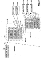
- FIG. 5 is an illustration of control blocks and a linked list scheme using a shared memory access scheme and of the present invention.
- a hardware register 151 contains the beginning address of a memory control block 155.
- a linked list mechanism allows for seamless transfers.
- control block 155 resides in memory as a linked list, its last entry there is a pointer to a second control block 165.
- Memory access is provided by the processor 313 or the SMA 315.
- the hardware register 151 has the beginning address of control block 155, which is loaded with parameters and data. In operation, consecutive memory accesses by the SMA 315 or the processor 315 allow data transfers to and from the composite blocks.
- the first set of parameters 154 in control block 155 starts at address 0100h.
- a memory address pointer is first set to 0100h and parameters 154 are transferred.
- the memory address pointer is incremented to the next memory address, which is 0104h and parameters 157 are transferred. This process is repeated until the memory addressing reaches address 0118h.
- the processor 313 or SMA 315 either by initial set up or a by a flag in the data located at 011C8h swaps the memory address pointer with the first address of data block_1 162.
- the data in data block_1 is then sequentially transferred.
- the memory address pointer is then swapped back and incremented and points to address 0120h of control block 155, which also swaps the memory address pointers to sequentially acquire additional data from data block_2 164.
- the memory address pointer Upon returning from data block_2 164, the memory address pointer is at 0124h which is the Next_Chain_Address 160.
- the data located at this address is the first address of to the next control block 165, which also comprises parameters 166 and data block addresses 168-174 pointing to data blocks 176-180, respectively.
- a flag 174 At the end of this linked list is a flag 174 indicating the end of the link lists.
- FIG. 10 An illustration of a preferred block loading process from the shared memory 315 is illustrated in Figure 10.
- timing issues associated with write accesses to dual port memories. Contentions come about when two or more entities try to access the same memory region, especially when performing a write operation.
- One possible preferred approach to resolve this problem is to allow control block writes when the composite/transport processor is idle.
- SMA shared memory access
- a preferred embodiment for physical layer processing for transmission in TDD mode is described as follows to illustrate the parameterization of the control blocks.
- the control blocks transmit transport channel processor 307, transmit composite channel processor 309, and transmit chip-rate processor 311 are utilized.
- First blocks of data are sent to the transmit transport channel processor 307 block from the shared memory 315.
- Transport blocks are generated and a cyclical redundancy check (CRC) is added at CRC attachment processor 42 to each new transport block.
- CRC cyclical redundancy check
- typical CRC types are generated, including none, 8, 12, 16 and 24 bit CRCs.
- Table 1 is a list of software parameters which is loaded into transmit transport channel processor 307 block.
- Transport Block Size Number of bits in last 32-bit input word. 0 means 32. : Number of bits per transport block. Rounded up to the next multiple of 32.
- Coder Input Size Number of total bits input to the coder minus one.
- Coder Output Size Number of total 32-bit words output from the first interleaver.
- Coding Block Size Number of bits per coder block.
- Coding Block Filler Bits Number of filler bits in the first code block.
- Turbo Interleaver Control the Number of rows in the transport channel. : Primitive Root. : Prime Number. Turbo Interleaver Prime Number Table Prime Number table for the turbo interleaver (10 words). Interleaver Memory Addresses Frame destination addresses, 8 addresses regardless of TTI.
- Transport Block Memory Addresses Transport block source addresses. One per transport block. Next TrCH Control Block Address/End Pointer to the control block for the next transport channel (if there are more to process).
- a NULL (value of 0) pointer with bit 31 set indicates that there are no more transport channels (i.e. a value of 0x80000000 is always used to indicate the last transport channel.
- the TrBlk concatenation/code block segmentation processor 44 creates a transmission time interval's (TTI's) worth of transport blocks, where the number of the blocks depends on the transport format selected for a particular Transmit channel.
- the segmentation processor 44 also concatenates the blocks into a single entity.
- Code blocks for the given transport channel are delivered to the channel coder processor 46. Depending on the coding type for the given transport channel, specified in the input data file, they are delivered to the appropriate channel coder function. Referring to Table 1, bits 10 and 11 are set to the desired type of coding. If the bits are set to 00, there is no coding. If the bits are set to 01, 10 and 11, the coding is Rate 1/2 convolutional, Rate 1/3 convolutional and Turbo, respectfully.
- the types of coding which are possible in the preferred embodiment are defined by the 3GPP TSG-RAN "Muliplexing and Channel Coding" 3GPP TS 25.212.
- This parameterizable hardware based approach allows for coding at a high performance level, for example, one clock per bit for convolutional encoding and two clocks per bit for Turbo Encoding. This is ten to one-hundred times faster (per clock rate) than the same function is typically performed in software.
- the coded blocks are processed in sequence by a rate matching process in the radio frame equalization 45 process. This effectively implements a concatenation of encoded blocks.
- the output is then sent to a first interleaver 50 process.
- the interleaving depends on the TTI interleaver rate which is also a software parameter in Table 1. For example, a 00 is set into bits 8 and 9 of the Quality of Service register for an interleave of 10 milliseconds. For 20, 40 and 80 ms TTIs, values of 01, 10 and 11, respectively, are set into bits 8 and 9.
- the data is segmented in the radio frame segmentation process 50 and returned to the shared memory 315 ready for the transmit composite channel processor 309 block.
- the transmit composite channel processor 309 block extracts data from the shared memory 315 along with control parameters and produces physical channel data.
- a radio frame's worth of data is complied from the data output from the previous block's first interleaver for the given transport channel.
- Table 2 is a format parameter table of the transmit composite channel processor's 309 control block.
- Table 2 TrCH Control Block Parameters Description Number Bits Before Rate Matching This Trch The Number of bits in the current column (frame) of the First Interleaver Buffer for this TrCH. Number Leftover Bits This Trch The Number of bits at the tail of the transport channel that are not considered for puncturing or repeating. Used for Turbo puncture, P2 bits.
- Rate Matching Direction Indicates whether the bit sequences is ⁇ S,P1,P2 ⁇ (forward) or ⁇ P2,P1,S ⁇ (reverse) Used for Turbo puncture, P2 bits.
- Rate Matching Type Indicates TURBO_PUNCTURE, REPEAT, NON_TURBO_PUNCTURE, or NONE.
- Rate Matching Column Top Indicates whether the first bit in the column is a systematic (S), parity 1(P1), or parity 2 (P2) bit.
- std_e_initl The initial value of the rate matching parameter for the first sequence.
- std_e_plus1 The increment value to the error when a bit is punctured or repeated.
- std_e_minusl The decrement value to the error when a bit is read from the First Interleaver Buffer.
- std_e_init2 The initial value of the rate matching parameter for the second sequence. Used for Turbo puncture, P2 bits. std_e_plus2 The increment value to the error when a bit is punctured or repeated. Used for Turbo puncture, P2 bits. std_e_minus2 The decrement value to the error when a bit is read from the First Interleaver Buffer. Used for Turbo puncture, P2 bits. Start Address This Trch The starting memory address of the transport channel.
- the rate matching type parameter uses bits 28 and 29. When these bits are set to 00, this indicates TURBO_PUNCTURE mode. Likewise, REPEAT, NON_TURBO_PUNCTURE, and NONE are represented by placing 01, 10 and 11, respectively into bit locations 28 and 29 of the parameter register.
- the data is rate matched by rate matching process 52 before it is multiplexed with other channels at the transport channel (TrCH) multiplexing process 54.
- the output of the multiplex transport channel processor 54 is segmented into physical channels in the physical channel (PyCH) 57 processor.
- a second interleaving is performed by the second interleaving processor 46 and mapped into physical channels at the physical channel processor 62.
- the transmit channel processed data is then returned to the shared memory 315 for further processing by the transmit chip-rate processor.
- the transmit chip-rate processor 311 block then extracts data and control parameters from the shared memory 315.
- the block 311 performs spreading, scrambling, gain application, formatting, preamble insertion, RRC filtering and produces one to sixteen resource units per time slot.
- the I and Q output of the transmit chip-rate processor 311 is ready for transmission.
- Figure 11 illustrates a preferred transmit configuration timeline 500 and show the advantages of the reparamatizable hardware implementation.
- the frames are bound by Frame Markers 503 on the Message Timeline 502.
- the data for the transmission must be configured during Frame N-2 505 before the processing is started at Execute_N 510.
- the data for Frame N is processed during Frame N-1 and must be completely finished processing and ready to transmit by Frame Marker 503(n).
- the frame hardware of the transmit channel is configured.
- the start control signal is sent from the SMA 313 to start the block processing from the database.
- the processing is performed in the transmit transport channel processor 307 and transmit composite channel processor 309, which make up the transmit frame receive processors.
- the transmit chip processor 311 is processing the data it received from the database.
- Figure 12 is an illustration of a preferred flow of data for FDD transmission.
- the transport channel is encoded and interleaved by a factor of four into two physical channels.
- the raw data for transport channel_1 102 and transport channel_2 104 are SMA transferred to the transport channel processing 106 where the CRC is added and the data is segmented into code blocks.
- the blocks are encoded, rate matched and a first interleaving is performed.
- the data as blocks of transmit channel data 108 - 122 are sent to the shared memory.
- the data is then sent to composite channel processing 124 where it is rate matched, second interleaved and segmented into physical channels at the rate of once per frame.
- the Physical Channel data is sent to the shared memory ordered as physical channels by frame 126 - 128.
- the physical channels by frame data is then sent to the Chip Rate Processing 130 where it is spread scrambled and filtered on a per frame basis.
- a control channel is also appended to each generated frame.
- a series of "jobs" for each channel processor are scheduled by software and presented to the processors via linked list job queues maintained in the shared memory.
- Each processing unit receives "jobs" via control blocks that reside in the shared memory.
- the content of each control block is a function of the unit for which it controls.
- the data and the order of the data is defined by the functionality and the specifications of each unit.
- Entries in each control block include control parameters for the unit and addresses which point to input data and addresses to output data locations. Control blocks can be linked together reducing control processor overhead.
- Table 3 Name Description il2 Disable Second Interleaver disable. Descr Disable Descrambler disable. Number TrCH Number of TrCH in the CCTrCH. Number Interleaver Blocks Number of ILBs in the CCTrCH. Interleaver Block Size Number of bits in this ILB. Number Ts Blocks Number of time slots in the ILB. Number Full Columns Number of full columns in the second interleaver matrix. Number Rows Number of rows in the interleaver array of 30 columns. Ts Block Size Time slot data block size in bits. Number resource units (RUs) Number of RUs in the time slot. RU Size RU data block size (number of soft decisions).
- RUs resource units
- RU ConsecutiveSize Number of consecutive soft bits read from RU.
- RU Offset Offset from the start of the first data word of an RU which has data mapped in reverse order.
- RU Address Start address of the RU data.
- RU Direction Data for an RU can be mapped in Forward or Reverse order.
- bit 16 of the "12 Disable" would be set to a 1.
- Control parameters and blocks of data are transferred from the shared memory 315 to the receive composite channel processor 303 block.
- Figure 13 represents the receive configuration timeline 700.
- the frames are bound by frame markers 703 on the message timeline 702.
- the received data is processed during frames Frame N+1 711 and Frame N +2 713.
- the received data is ready for high layer processing.
- the software parameters for hardware configuration for a particular received frame must be available in the pending database.
- the receive chip rate processor 301 places the data into the database.
- the received frame processor which are comprised of the receive composite channel processor 303 and receive transport channel processor 305 process the received data and subsequently sends the data on to higher layers.
Landscapes
- Engineering & Computer Science (AREA)
- Computer Networks & Wireless Communication (AREA)
- Signal Processing (AREA)
- Mobile Radio Communication Systems (AREA)
- Communication Control (AREA)
- Stored Programmes (AREA)
- Electrotherapy Devices (AREA)
- Transceivers (AREA)
- Time-Division Multiplex Systems (AREA)
Applications Claiming Priority (2)
| Application Number | Priority Date | Filing Date | Title |
|---|---|---|---|
| US37276302P | 2002-04-15 | 2002-04-15 | |
| EP03719734A EP1495567B1 (fr) | 2002-04-15 | 2003-04-15 | Blocs de commande pouvant etre parametres par logiciel utilisés dans le traitement de couche physique |
Related Parent Applications (2)
| Application Number | Title | Priority Date | Filing Date |
|---|---|---|---|
| EP03719734A Division EP1495567B1 (fr) | 2002-04-15 | 2003-04-15 | Blocs de commande pouvant etre parametres par logiciel utilisés dans le traitement de couche physique |
| EP03719734.0 Division | 2003-04-15 |
Publications (2)
| Publication Number | Publication Date |
|---|---|
| EP1755233A2 true EP1755233A2 (fr) | 2007-02-21 |
| EP1755233A3 EP1755233A3 (fr) | 2012-10-03 |
Family
ID=27789178
Family Applications (2)
| Application Number | Title | Priority Date | Filing Date |
|---|---|---|---|
| EP06122605A Withdrawn EP1755233A3 (fr) | 2002-04-15 | 2003-04-15 | Blocs de commande pouvant être parametrés par logiciel utilisés dans le traitement de couche physique |
| EP03719734A Expired - Lifetime EP1495567B1 (fr) | 2002-04-15 | 2003-04-15 | Blocs de commande pouvant etre parametres par logiciel utilisés dans le traitement de couche physique |
Family Applications After (1)
| Application Number | Title | Priority Date | Filing Date |
|---|---|---|---|
| EP03719734A Expired - Lifetime EP1495567B1 (fr) | 2002-04-15 | 2003-04-15 | Blocs de commande pouvant etre parametres par logiciel utilisés dans le traitement de couche physique |
Country Status (14)
| Country | Link |
|---|---|
| US (2) | US7496074B2 (fr) |
| EP (2) | EP1755233A3 (fr) |
| JP (3) | JP2005522963A (fr) |
| KR (6) | KR100626195B1 (fr) |
| CN (2) | CN2710288Y (fr) |
| AT (1) | ATE350822T1 (fr) |
| AU (1) | AU2003223595A1 (fr) |
| CA (1) | CA2482616A1 (fr) |
| DE (2) | DE20305986U1 (fr) |
| ES (1) | ES2276058T3 (fr) |
| HK (1) | HK1060493A2 (fr) |
| NO (1) | NO20044923L (fr) |
| TW (6) | TWI245512B (fr) |
| WO (1) | WO2003090011A2 (fr) |
Cited By (6)
| Publication number | Priority date | Publication date | Assignee | Title |
|---|---|---|---|---|
| CN101953095A (zh) * | 2008-02-20 | 2011-01-19 | Lg电子株式会社 | 处理填充式缓冲区状态报告的方法和装置 |
| EP2073396A3 (fr) * | 2007-12-20 | 2011-06-08 | Mediatek Inc. | Traitement en liaison montante dans un système TD-SCDMA |
| US8094641B2 (en) | 2007-12-20 | 2012-01-10 | Mediatek Inc. | TD-SCDMA uplink processing |
| US8391267B2 (en) | 2007-12-20 | 2013-03-05 | Mediatek Inc. | TD-SCDMA uplink processing for synchronization of signals at base station receiver |
| US8934502B2 (en) | 2008-02-20 | 2015-01-13 | Lg Electronics Inc. | Method and apparatus for processing padding buffer status reports |
| WO2015044733A1 (fr) * | 2013-09-30 | 2015-04-02 | Telefonaktiebolaget L M Ericsson (Publ) | Traitement de couche physique en liaison descendante dans des réseaux sans fil avec mappage de débit de symboles |
Families Citing this family (59)
| Publication number | Priority date | Publication date | Assignee | Title |
|---|---|---|---|---|
| FR2797736B1 (fr) * | 1999-08-19 | 2001-10-12 | Mitsubishi Electric France | Procede de configuration d'un systeme de telecommunications |
| US7583619B2 (en) | 2002-12-16 | 2009-09-01 | Nortel Networks Limited | Wireless access communications network |
| US7706347B2 (en) * | 2003-05-15 | 2010-04-27 | Lg Electronics Inc. | Signal processing apparatus and method using multi-output mobile communication system |
| KR101000388B1 (ko) * | 2003-05-15 | 2010-12-13 | 엘지전자 주식회사 | 이동 통신 시스템 및 이 이동 통신 시스템에서 신호를처리하는 방법 |
| KR101123724B1 (ko) * | 2004-05-18 | 2012-03-15 | 에스티 에릭슨 에스에이 | Umts 모바일 수신기에서의 수송 채널 디코딩 관리 |
| EP1779553A4 (fr) * | 2004-07-26 | 2008-02-20 | Interdigital Tech Corp | Co-processeur haute vitesse d'acces a des paquets descendants accroissant les capacites d'un modem hote existant |
| US7831890B2 (en) | 2004-10-12 | 2010-11-09 | Aware, Inc. | Resource sharing in a telecommunications environment |
| KR100647724B1 (ko) * | 2004-10-28 | 2006-11-28 | 주식회사알에프윈도우 | 이동형 무선 사설교환장치 |
| KR100663488B1 (ko) * | 2004-10-29 | 2007-01-02 | 삼성전자주식회사 | 재구성가능한 하드웨어 구조를 가지는 통신시스템 및 그에의한 재구성 방법 |
| US7929410B2 (en) * | 2005-06-29 | 2011-04-19 | Interdigital Technology Corporation | Protocol engine for processing data in a wireless transmit/receive unit |
| CN1893342B (zh) * | 2005-07-05 | 2010-06-09 | 上海原动力通信科技有限公司 | 多载波hsdpa的业务传输信道编码方法和编码装置 |
| GB2418806B (en) * | 2005-08-19 | 2006-09-27 | Ipwireless Inc | Duplex operation in a cellular communication system |
| KR100912784B1 (ko) | 2006-01-05 | 2009-08-18 | 엘지전자 주식회사 | 데이터 송신 방법 및 데이터 재전송 방법 |
| KR101265628B1 (ko) | 2006-01-05 | 2013-05-22 | 엘지전자 주식회사 | 이동 통신 시스템에서의 무선 자원 스케줄링 방법 |
| KR101203841B1 (ko) | 2006-01-05 | 2012-11-21 | 엘지전자 주식회사 | 무선 통신 시스템에서의 페이징 메시지 전송 및 수신 방법 |
| KR101211807B1 (ko) | 2006-01-05 | 2012-12-12 | 엘지전자 주식회사 | 이동통신 시스템에서 무선단말의 동기상태 관리방법 |
| EP1980062A4 (fr) | 2006-01-05 | 2011-03-30 | Lg Electronics Inc | Transmission de donnees dans un systeme de communication mobile |
| KR101187076B1 (ko) | 2006-01-05 | 2012-09-27 | 엘지전자 주식회사 | 이동 통신 시스템에 있어서 신호 전송 방법 |
| US7881724B2 (en) | 2006-01-05 | 2011-02-01 | Lg Electronics Inc. | Allocating radio resources in mobile communications system |
| US9456455B2 (en) | 2006-01-05 | 2016-09-27 | Lg Electronics Inc. | Method of transmitting feedback information in a wireless communication system |
| CN105515736A (zh) | 2006-01-05 | 2016-04-20 | Lg电子株式会社 | 在移动通信系统中发送数据 |
| KR101319870B1 (ko) | 2006-01-05 | 2013-10-18 | 엘지전자 주식회사 | 이동 통신 시스템에서의 핸드오버 방법 |
| US8493854B2 (en) | 2006-02-07 | 2013-07-23 | Lg Electronics Inc. | Method for avoiding collision using identifier in mobile network |
| KR101387475B1 (ko) | 2006-03-22 | 2014-04-22 | 엘지전자 주식회사 | 복수의 네트워크 엔터티를 포함하는 이동 통신시스템에서의 데이터 처리 방법 |
| US7447846B2 (en) | 2006-04-12 | 2008-11-04 | Mediatek Inc. | Non-volatile memory sharing apparatus for multiple processors and method thereof |
| US8335956B2 (en) | 2006-04-12 | 2012-12-18 | Tq Delta, Llc | Packet retransmission and memory sharing |
| EP2618517B1 (fr) | 2006-06-21 | 2023-08-02 | LG Electronics Inc. | Procédé de prise en charge de retransmission de données dans un système de communication mobile |
| KR20070121505A (ko) | 2006-06-21 | 2007-12-27 | 엘지전자 주식회사 | 무선링크 재설정 방법 |
| CN101595693B (zh) * | 2006-06-23 | 2013-01-23 | Lg电子株式会社 | 在无线通信系统中有效率地使用资源的方法 |
| US20070299297A1 (en) * | 2006-06-26 | 2007-12-27 | Robert Jarvik | Textured conforming shell for stabilization of the interface of precision heart assist device components to tissues |
| US20080019336A1 (en) * | 2006-07-24 | 2008-01-24 | Provigent Ltd. | Point-to-point link using partial transmit time periods on separate transmit and receive frequencies |
| US9008002B2 (en) | 2006-08-07 | 2015-04-14 | Qualcomm Incorporated | Conditional requests for asynchronous wireless communication |
| US8340027B2 (en) | 2006-08-07 | 2012-12-25 | Qualcomm Incorporated | Monitor period for asynchronous wireless communication |
| US8416762B2 (en) | 2006-08-07 | 2013-04-09 | Qualcomm Incorporated | Message exchange scheme for asynchronous wireless communication |
| US8310996B2 (en) | 2006-08-07 | 2012-11-13 | Qualcomm Incorporated | Conditional scheduling for asynchronous wireless communication |
| US8737313B2 (en) | 2006-08-07 | 2014-05-27 | Qualcomm Incorporated | Transmit time segments for asynchronous wireless communication |
| US8576807B2 (en) * | 2007-06-25 | 2013-11-05 | Qualcomm Incorporated | Channel interleaving structure for a wireless communication system |
| US7844217B2 (en) | 2007-10-01 | 2010-11-30 | Provigent Ltd. | Point-to-multipoint communication terminal having a single RF chain |
| TW201342962A (zh) * | 2007-10-18 | 2013-10-16 | Interdigital Tech Corp | 高茲料率應用之umts fdd數據機優化 |
| US7945217B2 (en) | 2007-11-13 | 2011-05-17 | Provigent Ltd. | Multi-mode baseband-IF converter |
| JP5643650B2 (ja) | 2007-11-21 | 2014-12-17 | コスモシド・インコーポレーテッド | ゲノム同定システム |
| US7991368B2 (en) | 2007-12-27 | 2011-08-02 | Provigent Ltd | Integrated RF-IF converter |
| WO2009096658A1 (fr) | 2008-01-31 | 2009-08-06 | Lg Electronics Inc. | Procédé de détermination de taille de bloc de transport et procédé de transmission de signaux utilisant ledit procédé |
| KR101526990B1 (ko) * | 2008-01-31 | 2015-06-11 | 엘지전자 주식회사 | 전송 블록 크기 결정 방법 및 이를 이용한 신호 전송 방법 |
| US8576955B2 (en) * | 2008-03-28 | 2013-11-05 | Qualcomm Incorporated | Architecture to handle concurrent multiple channels |
| US8537750B2 (en) * | 2009-06-02 | 2013-09-17 | Futurewei Technologies, Inc. | System and method for transport block size design for multiple-input, multiple-output (MIMO) in a wireless communications system |
| US8873582B2 (en) | 2010-04-08 | 2014-10-28 | Lg Electronics Inc. | Method for transmitting PPDU in wireless local area network and apparatus for the same |
| CN102237953B (zh) * | 2010-05-05 | 2014-06-11 | 中兴通讯股份有限公司 | 一种lte下行业务信道解速率匹配的方法及装置 |
| JP2012099989A (ja) * | 2010-11-01 | 2012-05-24 | Fujitsu Ltd | 無線通信装置および復号処理方法 |
| TWI551174B (zh) * | 2010-12-31 | 2016-09-21 | 電信科學技術研究院 | 使用者設備雙工規格訊息之獲取方法及設備 |
| US8406709B2 (en) | 2011-02-27 | 2013-03-26 | Provigent Ltd. | Carrier recovery in re-modulation communication systems |
| US9480077B2 (en) | 2011-06-06 | 2016-10-25 | Telefonaktiebolaget Lm Ericsson (Publ) | Methods and systems for a generic multi-radio access technology |
| US8989577B2 (en) | 2012-06-21 | 2015-03-24 | Qualcomm Incorporated | Methods and systems for implementing time-division duplexing in the physical layer |
| US9071358B2 (en) | 2012-06-21 | 2015-06-30 | Qualcomm Incrorporated | Repeater fiber-coax units |
| US9363017B2 (en) | 2012-07-06 | 2016-06-07 | Qualcomm Incorporated | Methods and systems of specifying coaxial resource allocation across a MAC/PHY interface |
| CN103580816B (zh) * | 2012-08-03 | 2018-05-15 | 中兴通讯股份有限公司 | 一种上行接收方法及装置 |
| US11272380B2 (en) | 2016-12-13 | 2022-03-08 | Qualcomm Incorporated | Methods and apparatus for managing code block interleaving |
| TWI694331B (zh) * | 2018-12-28 | 2020-05-21 | 瑞昱半導體股份有限公司 | 共享記憶體的雙模網路通訊裝置 |
| CN113904736B (zh) * | 2021-09-18 | 2023-05-23 | 中国电子科技集团公司第二十九研究所 | 一种多通道射频信号路由装置 |
Family Cites Families (26)
| Publication number | Priority date | Publication date | Assignee | Title |
|---|---|---|---|---|
| JP2853727B2 (ja) * | 1994-02-22 | 1999-02-03 | 日本ビクター株式会社 | 再生プロテクト方法及びプロテクト再生装置 |
| US5546420A (en) * | 1994-04-29 | 1996-08-13 | At&T Corp. | Methods of and devices for enhancing communications that use spread spectrum technology by using variable code techniques |
| US5959980A (en) * | 1995-06-05 | 1999-09-28 | Omnipoint Corporation | Timing adjustment control for efficient time division duplex communication |
| JP2910990B2 (ja) | 1995-11-09 | 1999-06-23 | エヌ・ティ・ティ移動通信網株式会社 | 移動通信システム用送受信機 |
| EP0773639B1 (fr) | 1995-11-09 | 2003-09-24 | NTT DoCoMo, Inc. | Transmetteur-récepteur pour système de communication mobile avec multiplexage fréquentiel duplex (FDD) et multiplexage temporel duplex (TDD) |
| JPH09187075A (ja) * | 1996-01-08 | 1997-07-15 | Canon Inc | 無線通信システム |
| JP3411150B2 (ja) | 1996-03-22 | 2003-05-26 | 松下電器産業株式会社 | Cdmaセルラ無線通信装置 |
| US6178235B1 (en) * | 1996-12-13 | 2001-01-23 | Telefonaktiebolaget Lm Ericsson | Dynamic traffic distribution |
| US6185704B1 (en) * | 1997-04-11 | 2001-02-06 | Texas Instruments Incorporated | System signaling schemes for processor and memory module |
| US5987010A (en) * | 1997-05-15 | 1999-11-16 | Advanced Micro Devices, Inc. | System and method for providing FDD and TDD modes of operation for a wireless communications device |
| US6351458B2 (en) * | 1997-09-22 | 2002-02-26 | Matsushita Electric Industrial Co., Ltd. | CDMA cellular wireless communication system |
| US6157989A (en) * | 1998-06-03 | 2000-12-05 | Motorola, Inc. | Dynamic bus arbitration priority and task switching based on shared memory fullness in a multi-processor system |
| US6434649B1 (en) * | 1998-10-14 | 2002-08-13 | Hitachi, Ltd. | Data streamer |
| JP2000175244A (ja) | 1998-12-08 | 2000-06-23 | Matsushita Electric Ind Co Ltd | 無線通信装置及び無線通信方法 |
| JP3593648B2 (ja) * | 1999-04-02 | 2004-11-24 | 富士通株式会社 | チャネルコード・デコード装置及び基地局 |
| JP2001094490A (ja) | 1999-09-22 | 2001-04-06 | Matsushita Electric Ind Co Ltd | 基地局装置及び受信信号処理方法 |
| US6968190B1 (en) * | 1999-11-29 | 2005-11-22 | Nokia Mobile Phones, Ltd. | Transfer of optimization algorithm parameters during handover of a mobile station between radio network subsystems |
| EP1111843A3 (fr) * | 1999-12-22 | 2003-03-26 | AT&T Corp. | Système et méthode pour coordonner de réseaux sans fil |
| FI19992810A7 (fi) | 1999-12-29 | 2001-06-30 | Nokia Corp | Lähetin/vastaanotin ja menetelmä RF-signaalin vastaanottamiseksi lähetin/vastaanottimessa |
| JP3413815B2 (ja) * | 2000-01-04 | 2003-06-09 | 独立行政法人通信総合研究所 | 無線装置 |
| JP3343573B2 (ja) * | 2000-01-04 | 2002-11-11 | 独立行政法人通信総合研究所 | 変復調特性を変更可能な無線装置 |
| US20020031166A1 (en) | 2000-01-28 | 2002-03-14 | Ravi Subramanian | Wireless spread spectrum communication platform using dynamically reconfigurable logic |
| JP2002010339A (ja) * | 2000-06-23 | 2002-01-11 | Ntt Docomo Inc | チャネル割当方法および通信装置 |
| JP4523708B2 (ja) | 2000-09-05 | 2010-08-11 | 株式会社日立国際電気 | Cdma基地局装置 |
| US6940827B2 (en) * | 2001-03-09 | 2005-09-06 | Adaptix, Inc. | Communication system using OFDM for one direction and DSSS for another direction |
| US7613167B2 (en) * | 2001-09-27 | 2009-11-03 | Broadcom Corporation | Method and system for upstream priority lookup at physical interface |
-
2003
- 2003-04-14 TW TW092108591A patent/TWI245512B/zh not_active IP Right Cessation
- 2003-04-14 TW TW092128346A patent/TWI280755B/zh not_active IP Right Cessation
- 2003-04-14 TW TW098131296A patent/TW201031157A/zh unknown
- 2003-04-14 DE DE20305986U patent/DE20305986U1/de not_active Expired - Lifetime
- 2003-04-14 TW TW092205813U patent/TW590340U/zh not_active IP Right Cessation
- 2003-04-14 TW TW096109403A patent/TW200807982A/zh unknown
- 2003-04-14 TW TW095113699A patent/TWI315135B/zh not_active IP Right Cessation
- 2003-04-15 JP JP2003586688A patent/JP2005522963A/ja active Pending
- 2003-04-15 HK HK03102741A patent/HK1060493A2/xx not_active IP Right Cessation
- 2003-04-15 CN CNU032443013U patent/CN2710288Y/zh not_active Expired - Lifetime
- 2003-04-15 EP EP06122605A patent/EP1755233A3/fr not_active Withdrawn
- 2003-04-15 DE DE60310905T patent/DE60310905T2/de not_active Expired - Lifetime
- 2003-04-15 KR KR1020047016431A patent/KR100626195B1/ko not_active Expired - Fee Related
- 2003-04-15 CN CN038084422A patent/CN1647429B/zh not_active Expired - Fee Related
- 2003-04-15 EP EP03719734A patent/EP1495567B1/fr not_active Expired - Lifetime
- 2003-04-15 AU AU2003223595A patent/AU2003223595A1/en not_active Abandoned
- 2003-04-15 ES ES03719734T patent/ES2276058T3/es not_active Expired - Lifetime
- 2003-04-15 CA CA002482616A patent/CA2482616A1/fr not_active Abandoned
- 2003-04-15 WO PCT/US2003/011415 patent/WO2003090011A2/fr not_active Ceased
- 2003-04-15 KR KR1020057015797A patent/KR100886729B1/ko not_active Expired - Fee Related
- 2003-04-15 KR KR20-2003-0011613U patent/KR200318729Y1/ko not_active Ceased
- 2003-04-15 US US10/414,125 patent/US7496074B2/en not_active Expired - Fee Related
- 2003-04-15 AT AT03719734T patent/ATE350822T1/de not_active IP Right Cessation
-
2004
- 2004-06-11 KR KR1020040043027A patent/KR100637781B1/ko not_active Expired - Fee Related
- 2004-11-11 NO NO20044923A patent/NO20044923L/no not_active Application Discontinuation
-
2005
- 2005-08-31 KR KR1020050080674A patent/KR20050095559A/ko not_active Withdrawn
-
2007
- 2007-03-08 JP JP2007059070A patent/JP2007228593A/ja active Pending
- 2007-10-15 JP JP2007268364A patent/JP2008104182A/ja active Pending
-
2008
- 2008-04-15 KR KR1020080034841A patent/KR20080041162A/ko not_active Withdrawn
-
2009
- 2009-02-23 US US12/390,719 patent/US8094653B2/en not_active Expired - Fee Related
Non-Patent Citations (1)
| Title |
|---|
| None |
Cited By (9)
| Publication number | Priority date | Publication date | Assignee | Title |
|---|---|---|---|---|
| EP2073396A3 (fr) * | 2007-12-20 | 2011-06-08 | Mediatek Inc. | Traitement en liaison montante dans un système TD-SCDMA |
| US8094641B2 (en) | 2007-12-20 | 2012-01-10 | Mediatek Inc. | TD-SCDMA uplink processing |
| US8391267B2 (en) | 2007-12-20 | 2013-03-05 | Mediatek Inc. | TD-SCDMA uplink processing for synchronization of signals at base station receiver |
| CN101953095A (zh) * | 2008-02-20 | 2011-01-19 | Lg电子株式会社 | 处理填充式缓冲区状态报告的方法和装置 |
| CN101953095B (zh) * | 2008-02-20 | 2013-06-05 | Lg电子株式会社 | 处理填充式缓冲区状态报告的方法和装置 |
| US8934502B2 (en) | 2008-02-20 | 2015-01-13 | Lg Electronics Inc. | Method and apparatus for processing padding buffer status reports |
| WO2015044733A1 (fr) * | 2013-09-30 | 2015-04-02 | Telefonaktiebolaget L M Ericsson (Publ) | Traitement de couche physique en liaison descendante dans des réseaux sans fil avec mappage de débit de symboles |
| US20150092671A1 (en) * | 2013-09-30 | 2015-04-02 | Telefonaktiebolaget L M Ericsson (Publ) | Downlink physical layer processing in wireless networks with symbol rate mapping |
| US9312994B2 (en) | 2013-09-30 | 2016-04-12 | Telefonaktiebolaget Lm Ericsson (Publ) | Downlink physical layer processing in wireless networks with symbol rate mapping |
Also Published As
Similar Documents
| Publication | Publication Date | Title |
|---|---|---|
| US8094653B2 (en) | Software parameterizable control blocks for use in physical layer processing | |
| US8391267B2 (en) | TD-SCDMA uplink processing for synchronization of signals at base station receiver | |
| CN101237241A (zh) | 一种实现混合自动请求重传处理和信道译码的方法和系统 | |
| US7437655B2 (en) | Apparatus and method for flexible data rate matching | |
| US20090161647A1 (en) | Td-scdma uplink processing | |
| EP1415489A1 (fr) | Architecture de station de base cellulaire a partionnement logiciel | |
| EP1472803B1 (fr) | Procede et arrangement pour le traitement asynchrone de donnees cctrch | |
| US8094641B2 (en) | TD-SCDMA uplink processing | |
| US20130019144A1 (en) | Wireless communication system, wireless communication apparatus, and wireless communication method | |
| KR20070042587A (ko) | 메모리 스택에 저장되는 인터리브된 데이터를 효율적으로할당 및 할당 해제하는 방법 및 장치 | |
| HK1074296A (en) | Software parameterizable control blocks for use in physical layer processing | |
| KR100377626B1 (ko) | 이동통신시스템에서 역다중화/다중화 구현을 위한기능블록 및 슬롯할당방법 | |
| EP1751901B1 (fr) | Gestion par decodage d'un canal de transmission dans un recepteur mobile umts | |
| CN101461139A (zh) | 高效配置及去配置储存于存储器堆栈交错数据的方法及装置 |
Legal Events
| Date | Code | Title | Description |
|---|---|---|---|
| PUAI | Public reference made under article 153(3) epc to a published international application that has entered the european phase |
Free format text: ORIGINAL CODE: 0009012 |
|
| 17P | Request for examination filed |
Effective date: 20061019 |
|
| AC | Divisional application: reference to earlier application |
Ref document number: 1495567 Country of ref document: EP Kind code of ref document: P |
|
| AK | Designated contracting states |
Kind code of ref document: A2 Designated state(s): AT BE BG CH CY CZ DE DK EE ES FI FR GB GR HU IE IT LI LU MC NL PT RO SE SI SK TR |
|
| AX | Request for extension of the european patent |
Extension state: AL BA HR MK YU |
|
| RIC1 | Information provided on ipc code assigned before grant |
Ipc: H04B 1/707 20060101ALN20070124BHEP Ipc: H04B 1/00 20060101AFI20070124BHEP |
|
| RIN1 | Information on inventor provided before grant (corrected) |
Inventor name: CASTOR, DOUGLAS R. Inventor name: MCCLELLAN, GEORGE W. Inventor name: LEVI, ALAN M. Inventor name: DESAI, BINISH Inventor name: BASS, DAVID Inventor name: STARSINIC, MICHAEL F. Inventor name: HEPLER, EDWARD, L. |
|
| PUAL | Search report despatched |
Free format text: ORIGINAL CODE: 0009013 |
|
| AK | Designated contracting states |
Kind code of ref document: A3 Designated state(s): AT BE BG CH CY CZ DE DK EE ES FI FR GB GR HU IE IT LI LU MC NL PT RO SE SI SK TR |
|
| AX | Request for extension of the european patent |
Extension state: AL MK |
|
| RIC1 | Information provided on ipc code assigned before grant |
Ipc: H04L 1/08 20060101ALI20120830BHEP Ipc: H04W 28/18 20090101ALN20120830BHEP Ipc: H04B 1/707 20110101ALN20120830BHEP Ipc: H04B 7/26 20060101ALI20120830BHEP Ipc: H04L 1/00 20060101ALI20120830BHEP Ipc: H04W 74/02 20090101ALN20120830BHEP Ipc: G06F 13/16 20060101ALI20120830BHEP Ipc: H04W 80/00 20090101ALN20120830BHEP Ipc: H04B 1/00 20060101AFI20120830BHEP Ipc: H04W 88/06 20090101ALI20120830BHEP Ipc: H04B 1/40 20060101ALI20120830BHEP |
|
| RAP1 | Party data changed (applicant data changed or rights of an application transferred) |
Owner name: INTERDIGITAL TECHNOLOGY CORPORATION |
|
| 17Q | First examination report despatched |
Effective date: 20130422 |
|
| AKX | Designation fees paid |
Designated state(s): AT BE BG CH CY CZ DE DK EE ES FI FR GB GR HU IE IT LI LU MC NL PT RO SE SI SK TR |
|
| GRAP | Despatch of communication of intention to grant a patent |
Free format text: ORIGINAL CODE: EPIDOSNIGR1 |
|
| RIC1 | Information provided on ipc code assigned before grant |
Ipc: H04L 1/08 20060101ALI20140313BHEP Ipc: H04B 1/40 20060101ALI20140313BHEP Ipc: H04W 80/00 20090101ALN20140313BHEP Ipc: H04B 7/26 20060101ALI20140313BHEP Ipc: G06F 13/16 20060101ALI20140313BHEP Ipc: H04W 28/18 20090101ALN20140313BHEP Ipc: H04B 1/00 20060101AFI20140313BHEP Ipc: H04W 88/06 20090101ALI20140313BHEP Ipc: H04L 1/00 20060101ALI20140313BHEP Ipc: H04W 74/02 20090101ALN20140313BHEP Ipc: H04B 1/707 20110101ALN20140313BHEP |
|
| INTG | Intention to grant announced |
Effective date: 20140324 |
|
| STAA | Information on the status of an ep patent application or granted ep patent |
Free format text: STATUS: THE APPLICATION IS DEEMED TO BE WITHDRAWN |
|
| 18D | Application deemed to be withdrawn |
Effective date: 20140805 |