EP1762858A2 - Erregerspulenansteuerung eines Magnetsensors - Google Patents
Erregerspulenansteuerung eines Magnetsensors Download PDFInfo
- Publication number
- EP1762858A2 EP1762858A2 EP06254741A EP06254741A EP1762858A2 EP 1762858 A2 EP1762858 A2 EP 1762858A2 EP 06254741 A EP06254741 A EP 06254741A EP 06254741 A EP06254741 A EP 06254741A EP 1762858 A2 EP1762858 A2 EP 1762858A2
- Authority
- EP
- European Patent Office
- Prior art keywords
- signal
- exciting coil
- drive signal
- amplifier
- magnetic sensor
- Prior art date
- Legal status (The legal status is an assumption and is not a legal conclusion. Google has not performed a legal analysis and makes no representation as to the accuracy of the status listed.)
- Granted
Links
- 238000005259 measurement Methods 0.000 claims description 13
- 230000004907 flux Effects 0.000 description 30
- 230000005284 excitation Effects 0.000 description 9
- 238000001514 detection method Methods 0.000 description 8
- 238000004519 manufacturing process Methods 0.000 description 8
- 230000010354 integration Effects 0.000 description 6
- 239000003990 capacitor Substances 0.000 description 5
- 238000000034 method Methods 0.000 description 5
- 229920006395 saturated elastomer Polymers 0.000 description 3
- 239000000696 magnetic material Substances 0.000 description 2
- 230000001360 synchronised effect Effects 0.000 description 2
- 238000004804 winding Methods 0.000 description 2
- 230000003321 amplification Effects 0.000 description 1
- 238000007796 conventional method Methods 0.000 description 1
- 230000000694 effects Effects 0.000 description 1
- 238000005516 engineering process Methods 0.000 description 1
- 238000009499 grossing Methods 0.000 description 1
- 239000000463 material Substances 0.000 description 1
- 239000002159 nanocrystal Substances 0.000 description 1
- 238000003199 nucleic acid amplification method Methods 0.000 description 1
- 230000010355 oscillation Effects 0.000 description 1
- 230000035945 sensitivity Effects 0.000 description 1
Images


Classifications
-
- G—PHYSICS
- G01—MEASURING; TESTING
- G01R—MEASURING ELECTRIC VARIABLES; MEASURING MAGNETIC VARIABLES
- G01R33/00—Arrangements or instruments for measuring magnetic variables
- G01R33/02—Measuring direction or magnitude of magnetic fields or magnetic flux
- G01R33/04—Measuring direction or magnitude of magnetic fields or magnetic flux using the flux-gate principle
Definitions
- the present invention relates generally to an exciting coil drive circuit of a magnetic sensor, and more particularly, to technology for providing a highly-accurate and stable exciting coil drive circuit of a magnetic sensor.
- a so-called flux gate magnetometer which saturates a magnetic flux by inputting periodical drive signals to an exciting coil wound on a soft magnetic core to measure intensity of an external magnetic field from saturation time intervals changed depending on the size of the external magnetic field that is measured.
- the flux gate magnetometer has various excellent features for a magnetometer, such as (1) high sensitivity and magnetic field resolution, (2) capability of measuring a weak magnetic field, (3) a wide measurement range, (4) temperature stability better than magnetometers of other modes, and (5) high linearity to an input magnetic field.
- Japanese Patent Application Laid-Open Publication No. 2005-147947 is an example of such a flux gate magnetometer and discloses a flux gate magnetometer with a magnetic sensor that excites a ring core composed of a magnetic detecting material up to a saturated magnetic field area by electrifying an exciting coil with an alternating signal to measure a magnetic flux density using symmetric property of a saturated magnetic flux density induced in the ring core.
- Japanese Patent Application Laid-Open Publication No. 1996-285929 discloses a magnetometer that supplies an excitation current from an oscillator to an exciting coil at a flux gate formed by winding the exciting coil and a detecting coil on a core to perform synchronous rectification of the output of the detecting coil with a synchronous rectification circuit.
- Japanese Patent Application Laid-Open Publication No. 2005-61969 discloses a flux gate magnetometer for accomplishing further improvement in accuracy in measurement of a magnetic force.
- High accuracy and stability are required for a drive circuit driving an exciting coil of a magnetic sensor used in the flux gate magnetometer.
- a plurality of flux gate magnetometers is often used at the same time and, therefore, manufacturing variations must be reduced in each flux gate magnetometer in the case of mass production.
- a smaller component count is required and a chip area must not be occupied at the time of integration.
- the present invention was conceived in consideration of such circumstances and it is therefore one object of the present invention to provide a highly-accurate and stable exciting coil drive circuit of a magnetic sensor having fewer manufacturing variations, which can be miniaturized.
- an exciting coil drive circuit of a magnetic sensor comprising a D/A converter that receives input of digital data for detecting a magnetic field; a first amplifier that outputs a drive signal P applied to one end of an exciting coil of the magnetic sensor based on the output signal of the D/A converter; and a second amplifier that outputs a drive signal N applied to the other end of the exciting coil based on the output signal of the D/A converter, the drive signal N being an inversion signal of the drive signal P, the drive signal N intersecting with the drive signal P twice or more.
- the exciting coil drive circuit of the magnetic sensor is digitally constituted by using the D/A converter, the drive circuit can be achieved which is less affected by external factors such as temperature changes. Therefore, the highly-accurate and stable drive signal can be generated.
- the manufacturing variations can be constrained at the time of mass production.
- an exciting coil drive circuit of a magnetic sensor comprising an SC integrator that receives input of digital data for detecting a magnetic field; a first amplifier that outputs a drive signal P applied to one end of an exciting coil of the magnetic sensor based on the output signal of the SC integrator; and a second amplifier that outputs a drive signal N applied to the other end of the exciting coil based on the output signal of the SC integrator, the drive signal N being an inversion signal of the drive signal P, the drive signal N intersecting with the drive signal P twice or more.
- the exciting coil is selected by the switch for the application of the drive signals, a plurality of the exciting coils can be driven by the same exciting coil drive circuit. Therefore, the manufacturing variations can be constrained. Since the exciting coil drive circuit is used in common, the component count and chip area of the drive circuit can be reduced.
- the present invention can thus provide a highly-accurate and stable exciting coil drive circuit of a magnetic sensor having fewer manufacturing variations, which can be miniaturized.
- FIG. 1 shows a configuration of a flux gate magnetometer described as one embodiment of the present invention.
- a flux gate magnetometer shown in Fig. 1 has three magnetic sensors 11, 12, 13 corresponding to the X-axis, Y-axis, and Z-axis, respectively.
- Each magnetic sensor 11, 12, 13 is constituted by winding an exciting coil 112, 122, 132 and a detecting coil 113, 123, 133 on a magnetic core 111, 121, 131 composed of a soft magnetic material such as a nanocrystal soft magnetic material.
- the exciting coil 112, 122, 132 is driven by an exciting coil drive circuit constituted by including an excitation switch circuit 21, a noninverting amplifier 22, an inverting amplifier 23, a D/A converter 24, and a control logic that controls the operation of the D/A converter 24 (hereinafter, DAC control logic 25).
- the output voltage of the detecting coil 113, 123, 133 is processed by a signal detecting circuit constituted by including a detection switch circuit 31, a voltage adjustment circuit 32 that adjusts the output voltage to a predetermined voltage level, a differential amplifier 33 that amplifies the output voltage, a hysteresis comparator 34 that outputs a low level digital signal in a period between two spike voltages included in the output voltage, and a counter 35 that counts the number of pulses of a clock signal in a period when the digital signal output from the hysteresis comparator 34 is in the low level.
- a signal detecting circuit constituted by including a detection switch circuit 31, a voltage adjustment circuit 32 that adjusts the output voltage to a predetermined voltage level, a differential amplifier 33 that amplifies the output voltage, a hysteresis comparator 34 that outputs a low level digital signal in a period between two spike voltages included in the output voltage, and a counter 35 that counts the number of pulses of a clock signal in
- a control circuit 41 controls the DAC control logic 25.
- the control circuit 41 receives and stores a count value input from the counter 35 into an internal memory 411.
- the control circuit 41 is connected to a control line 51 of the excitation switch circuit 21 and the detection switch circuit 31 and the control circuit 41 controls the opening/closing of the switch 21 and the switch 31 through the control line 51.
- the control circuit 41 is communicably connected to a microcomputer 71 (external apparatus) via a bus line 61 and transmits the count value stored in the memory 411 to the microcomputer 71 as needed.
- Fig. 2 is a timing chart of the operation of the flux gate magnetometer 1 of the embodiment. The operation of the flux gate magnetometer 1 will be described with reference to the timing chart of Fig. 2. In the following description, it is assumed that all the contacts of the excitation switch circuit 21 and the detection switch circuit 31 are opened (turned off) in advance.
- a measurement start signal is input from the microcomputer 71 to the control circuit 41 via the bus line 61 (t1).
- the control circuit 41 When inputting the measurement start signal, the control circuit 41 outputs a signal (hereinafter, x-axis selection signal) for turning on the x-axis contacts of the excitation switch circuit 21 and the detection switch circuit 31 (t2).
- x-axis selection signal When inputting the x-axis selection signal, the excitation switch circuit 21 and the detection switch circuit 31 turn on the contacts of the exciting coil 112 and the detecting coil 113 of the magnetic sensor 11 for measuring the magnetic field in the x-axis direction. In this way, the excitation switch circuit 21 selects the exciting coils 112, 122, 132 to which a drive signal P and a drive signal N are applied as described below.
- the control circuit 41 then outputs a drive start enable signal to the DAC control logic 25 (t3).
- DAC data are input to the D/A converter 24.
- down-count data are input as the DAC data (t4 to t5). Because of the down-count data, a signal is applied immediately before a step-up period to prevent the exciting coil 112 from generating a high-voltage back electromotive force causing damages of circuit elements such as the noninverting amplifier 22 and the inverting amplifier 23.
- the DAC control logic 25 then outputs up-count data to the D/A converter 24 for the DAC data (t5). In this way, the D/A converter 24 outputs a signal for a step-up period of a triangular wave (t5 to t8).
- the DAC control logic 25 stops the output of the up-count data to the D/A converter 24 at t8 and then outputs the down-count data. In this way, the D/A converter 24 outputs a signal for a step-down period of the triangular wave (t8 to t11).
- the DAC control logic 25 stops the output of the down-count data to the D/A converter 24 at t11 and then outputs the up-count data. Because of the down-count data, a signal is applied immediately after the step-down period to prevent the exciting coil from generating a high-voltage back electromotive force causing damages of circuit elements such as the noninverting amplifier 22 and the inverting amplifier 23.
- a drive signal of the D/A converter 24 is supplied to the noninverting input terminal of the noninverting amplifier 22.
- a Vref signal of the D/A converter 24 is supplied to the noninverting input terminal of the inverting amplifier 23.
- the output of the noninverting amplifier 22 is fed back negatively to the inverting input terminal of the noninverting amplifier 22.
- the output of the noninverting amplifier 22 is input to the inverting input terminal of the inverting amplifier 23.
- the noninverting amplifier 22 outputs a signal shown by a solid line of Fig. 2 (hereinafter, drive signal P), which is acquired by amplifying the output signal of the D/A converter 24, and the inverting amplifier 23 outputs a signal shown by a dotted line of Fig. 2 (hereinafter, drive signal N), which is acquired by inverting the oscillation of the drive signal P.
- the drive signal P output from the noninverting amplifier 22 is applied to one of two terminals of the exciting coil 112.
- the drive signal N output from the inverting amplifier 23 is applied to the other of two terminals of the exciting coil 112. Therefore, a difference voltage between the drive signal P and the drive signal N is applied to the exciting coil 112 (hereinafter, this voltage is referred to as an exciting voltage).
- spike voltages (t7, t10) generated between the terminals of the detecting coil 113 are caused by the electromotive force generated in a non-saturated section of a B-H curve (B: magnetic flux density, H: magnetic field) of the magnetic sensor 11.
- B magnetic flux density
- H magnetic field
- a time interval (Tx) of two spike voltages at t7 and t10 is changed depending on an external magnetic field ⁇ H applied to the magnetic sensor 11. That is, information about intensity, etc. of the external magnetic field ⁇ H can be acquired by measuring the time interval (Tx) of the output of the two spike voltages.
- the spike voltages generated in the detecting coil 113 are converted to predetermined voltage levels by the voltage adjustment circuit 32 and are input to the differential amplifier 33 for amplification.
- the output voltage amplified by the differential amplifier 33 is input to the hysteresis comparator 34.
- the hysteresis comparator 34 outputs a digital signal becoming low level in a period defined by adjacent spike voltages included in the output voltage and becoming high level in other periods. In an initial state, the hysteresis comparator 34 outputs the high level. The hysteresis comparator 34 starts the output of the low level at the timing of the input of the spike voltage generated due to the polarity inversion of the exciting voltage at t6 (t7). The hysteresis comparator 34 switches the output to the high level at the timing of the input of the spike voltage generated due to the polarity inversion of the exciting voltage at t9 (t10).
- the digital signal output from the hysteresis comparator 34 is input to the counter 35.
- the clock signal is input to the counter 35, and the counter 35 counts the number of pulses of the clock signal in a period when the digital signal output from the hysteresis comparator 34 is in the low level.
- the counter 35 outputs the count value to the control circuit 41.
- the control circuit 41 stores the input count value to the memory 411.
- the control circuit 41 then turns off the drive start enable signal that is input to the DAC control logic 25 (t13).
- the control circuit 41 stops the input of the X-axis selection signal to the excitation switch circuit 21 and the detection switch circuit 31 (t14). In this way, the contacts are turned off in the exciting coil 112 and the detecting coil 113 of the magnetic sensor 11 for measuring the magnetic field in the x-axis direction.
- the control circuit 41 then transmits a signal (hereinafter, Y-axis selection signal) for turning on the Y-axis contacts of the excitation switch circuit 21 and the detection switch circuit 31 (t15).
- a signal hereinafter, Y-axis selection signal
- the process for the Y-axis is started.
- the process for the Y-axis is performed in a period from t15 to t16 as is the case with the X-axis.
- the process for the Z-axis is also performed in a period from t17 to t18 as is the case with the X-axis.
- the control circuit 41 transmits to the microcomputer 71 an interrupt signal notifying that the writing of the count values is completed (t19).
- the microcomputer 71 transmits a read request to the control circuit 41.
- the microcomputer 71 reads the count value stored in the memory 411 of the control circuit 41 for each of the X-axis, Y-axis, and Z-axis (t 20).
- the count values read by the microcomputer 71 are utilized for measuring the intensity, etc. of the external magnetic field ⁇ H.
- the signals for driving the exciting coils 112, 122, 132 are generated with the digital circuits such as the DAC control logic 25 and the D/A converter 24. Therefore, the highly-accurate and stable drive signals are generated which are less affected by the temperature, etc., as compared to the case of using analog circuits. The manufacturing variations are also constrained by using the digital circuits.
- a plurality of the exciting coils 112, 122, 132 is driven by the same D/A converter 24. Therefore, the uniform exciting voltage can be applied to each of the exciting coils 112, 122, 132 and variations of the output can be constrained. Since the circuit is used in common, the component count and the chip area can be reduced at the time of integration.
- the lengths of the step-up period (t5 to t8) and the step-down period (t8 to t11) of the drive signal can be matched highly accurately to improve the measurement accuracy. Since some circuits necessary in the case of the analog circuit are not needed which are, for example, circuits measuring the overall lengths of the drive signals for correcting the effects of the measurement intervals of errors included in the time intervals (Tx, Ty, Tz), the small-sized flux gate magnetometer 1 with lower electric power consumption can be achieved.
- the flux gate magnetometer 1 of the embodiment counts the number of the pulses of the clock signal with the counter 35 to measure the time intervals (Tx, Ty, Tz) of two spike voltages, the measurement can be performed with accuracy higher than the case of using the analog circuits.
- an A/D converter occupying large chip area is generally needed at the time of integration if the analog circuits measure the time intervals (Tx, Ty, Tz), since the counter 35 is a counter 35 occupying small chip area, the small-sized flux gate magnetometer 1 can be achieved.
- the flux gate magnetometer 1 of the embodiment is less affected by temperature and noises since the output voltage of the detecting coil 113, 123, 133 is digitalized by the hysteresis comparator 33 at an early stage.
- the same differential amplifier 33 and the same hysteresis comparator 34 perform processes for the output voltages of a plurality of the detecting coils 113, 123, 133, variations are reduced in the measurement values of the detecting coils 113, 123, 133. Since the same circuits are used in the processes for the output voltages of the detecting coils 113, 123, 133 in this way, the component count and the chip area can be reduced at the time of integration.
- the differential amplifier 33 is used for amplifying the output voltages, less common-mode noise is mixed. Since the detecting coils 113, 123, and 133 are not grounded, this also prevents the common-mode noise from being mixed.
- a low-pass filter may be inserted at the stage after the D/A converter 24 to smooth the drive signal output from the D/A converter 24.
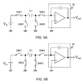
- the drive signal may be generated by an SC (switched capacitor) integrator with a configuration shown in Fig. 3 instead of the D/A converter 24.
- the SC integrator 80 shown in Fig. 3 is constituted by four switches SW1 to SW4, a capacitor C1, and an integration circuit 81 using an operational amplifier.
- the switch SW1, the capacitor C1, and SW4 are serially connected in this order; SW1 is connected to a direct-current power source Vin; and the output of SW4 is input to the noninverting input terminal of the operational amplifier constituting the integration circuit 81.
- the switch SW2 is connected between the switch SW1 and the capacitor C1 and one end of the switch SW2 is grounded.
- the switch SW3 is connected between the capacitor C1 and the switch SW4 and one end of the switch SW3 is grounded.
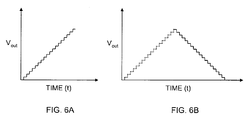
- the SC integrator 80 can match ⁇ t1 and ⁇ t2 accurately with the use of known digital circuits and can generate the exact triangular wave with the step-up period and the step-down period having inclinations matched highly accurately. Therefore, when the SC integrator 80 is used, the flux gate magnetometer 1 can also be achieved which can measure a magnetic field highly accurately as is the case with the D/A converter 24.
Landscapes
- Physics & Mathematics (AREA)
- Condensed Matter Physics & Semiconductors (AREA)
- General Physics & Mathematics (AREA)
- Measuring Magnetic Variables (AREA)
Applications Claiming Priority (1)
| Application Number | Priority Date | Filing Date | Title |
|---|---|---|---|
| JP2005264284A JP4856915B2 (ja) | 2005-09-12 | 2005-09-12 | 磁気センサの励磁コイル駆動回路 |
Publications (3)
| Publication Number | Publication Date |
|---|---|
| EP1762858A2 true EP1762858A2 (de) | 2007-03-14 |
| EP1762858A3 EP1762858A3 (de) | 2009-05-06 |
| EP1762858B1 EP1762858B1 (de) | 2010-11-17 |
Family
ID=37591621
Family Applications (1)
| Application Number | Title | Priority Date | Filing Date |
|---|---|---|---|
| EP06254741A Not-in-force EP1762858B1 (de) | 2005-09-12 | 2006-09-12 | Erregerspulenansteuerung eines Magnetsensors |
Country Status (7)
| Country | Link |
|---|---|
| US (1) | US7355398B2 (de) |
| EP (1) | EP1762858B1 (de) |
| JP (1) | JP4856915B2 (de) |
| KR (1) | KR100804389B1 (de) |
| CN (1) | CN1932542B (de) |
| DE (1) | DE602006018231D1 (de) |
| TW (1) | TWI300850B (de) |
Cited By (2)
| Publication number | Priority date | Publication date | Assignee | Title |
|---|---|---|---|---|
| EP1762858B1 (de) * | 2005-09-12 | 2010-11-17 | Sanyo Electric Co., Ltd. | Erregerspulenansteuerung eines Magnetsensors |
| CN113359202A (zh) * | 2021-06-07 | 2021-09-07 | 中国地震局地球物理研究所 | 基于单片机的磁通门激励信号产生方法及磁通门激励电路 |
Families Citing this family (18)
| Publication number | Priority date | Publication date | Assignee | Title |
|---|---|---|---|---|
| JP4856916B2 (ja) * | 2005-09-12 | 2012-01-18 | オンセミコンダクター・トレーディング・リミテッド | 磁気センサの信号検出回路 |
| JP2008292325A (ja) * | 2007-05-24 | 2008-12-04 | Sanyo Electric Co Ltd | 信号検出回路 |
| JP2010199822A (ja) * | 2009-02-24 | 2010-09-09 | Panasonic Corp | 検波回路、物理量センサ装置 |
| JP5518661B2 (ja) * | 2010-09-30 | 2014-06-11 | 株式会社フジクラ | 半導体集積回路、磁気検出装置、電子方位計 |
| US9201122B2 (en) * | 2012-02-16 | 2015-12-01 | Allegro Microsystems, Llc | Circuits and methods using adjustable feedback for self-calibrating or self-testing a magnetic field sensor with an adjustable time constant |
| JP5364814B2 (ja) | 2012-05-15 | 2013-12-11 | 株式会社フジクラ | 磁気素子制御装置、磁気素子制御方法及び磁気検出装置 |
| JP5364816B1 (ja) | 2012-06-08 | 2013-12-11 | 株式会社フジクラ | 磁気素子制御装置、磁気素子制御方法及び磁気検出装置 |
| JP5393844B2 (ja) | 2012-06-08 | 2014-01-22 | 株式会社フジクラ | 磁気素子制御装置、磁気素子制御方法及び磁気検出装置 |
| JP6014544B2 (ja) * | 2013-05-13 | 2016-10-25 | 株式会社フジクラ | 磁界検出装置の検査用回路及びその検査方法 |
| US9261571B2 (en) * | 2013-08-15 | 2016-02-16 | Texas Instruments Incorporated | Fluxgate magnetic sensor readout apparatus |
| JP6280767B2 (ja) * | 2014-02-21 | 2018-02-14 | ルネサスエレクトロニクス株式会社 | 駆動回路 |
| US10801319B2 (en) * | 2015-04-30 | 2020-10-13 | Salunda Limited | Sensing of the contents of a bore |
| CN110557016B (zh) * | 2018-05-31 | 2021-07-30 | 西门子(深圳)磁共振有限公司 | 电源装置和磁共振成像系统 |
| FR3083321B1 (fr) * | 2018-06-27 | 2021-03-05 | Safran Electronics & Defense | Capteur de courant a vanne de flux |
| CN109612503B (zh) * | 2018-12-03 | 2020-12-29 | 重庆文理学院 | 一种磁传感器的励磁线圈驱动装置 |
| CN110376419B (zh) * | 2019-08-13 | 2021-06-01 | 上海联影医疗科技股份有限公司 | 超导磁体的励磁检测电路及其控制方法 |
| CN111610250B (zh) * | 2020-07-06 | 2023-09-05 | 管网集团(新疆)联合管道有限责任公司 | 一种智能剩磁检测试验装置 |
| CN113162594A (zh) * | 2021-03-12 | 2021-07-23 | 苏州贝昂科技有限公司 | 磁感应电路及电器设备 |
Citations (3)
| Publication number | Priority date | Publication date | Assignee | Title |
|---|---|---|---|---|
| JPH08285929A (ja) | 1995-04-19 | 1996-11-01 | Shimadzu Corp | 磁力計 |
| JP2005061969A (ja) | 2003-08-11 | 2005-03-10 | Asahi Kasei Electronics Co Ltd | 方位角計測装置及び方位角計測方法 |
| JP2005147947A (ja) | 2003-11-18 | 2005-06-09 | Meisei Electric Co Ltd | 磁気センサー用コア、磁気センサー及びフラックスゲート磁力計 |
Family Cites Families (20)
| Publication number | Priority date | Publication date | Assignee | Title |
|---|---|---|---|---|
| JPS63115231A (ja) * | 1986-10-31 | 1988-05-19 | Nok Corp | 関数信号発生装置 |
| JPH03272483A (ja) * | 1990-02-28 | 1991-12-04 | Nkk Corp | 磁気検出装置 |
| JP2617615B2 (ja) * | 1990-10-19 | 1997-06-04 | 日本鋼管株式会社 | 磁気測定方法およびその装置 |
| US5091697A (en) * | 1989-07-31 | 1992-02-25 | Ii Morrow, Inc. | Low power, high accuracy magnetometer and magnetic field strength measurement method |
| WO1991018299A1 (en) * | 1990-05-19 | 1991-11-28 | Nkk Corporation | Device for sensing magnetism |
| JPH0493781A (ja) * | 1990-08-10 | 1992-03-26 | Seiko Instr Inc | 三次元積分磁束計 |
| US5644851A (en) * | 1991-12-20 | 1997-07-08 | Blank; Rodney K. | Compensation system for electronic compass |
| JPH06303143A (ja) * | 1993-04-15 | 1994-10-28 | Matsushita Electric Ind Co Ltd | 積分型da変換器 |
| JP3360550B2 (ja) | 1996-10-17 | 2002-12-24 | 住友電気工業株式会社 | 磁気センサ駆動回路装置 |
| JP3063654B2 (ja) | 1996-12-06 | 2000-07-12 | 住友電気工業株式会社 | 磁気センサ用電圧増幅回路 |
| JP4007464B2 (ja) * | 1997-10-06 | 2007-11-14 | Tdk株式会社 | 磁気探知装置 |
| US6268725B1 (en) * | 1998-04-29 | 2001-07-31 | Medtronic, Inc. | Flux-gate magnetometer with drive signal for reducing effects of electromagnetic interference |
| US6222363B1 (en) * | 1999-01-08 | 2001-04-24 | Methode Electronics, Inc. | Switch-mode flux-gate magnetometer |
| DE69925573T2 (de) * | 1999-05-12 | 2006-04-27 | Asulab S.A. | Magnetischer F?hler hergestellt auf einem halbleitenden Substrat |
| US6218831B1 (en) * | 1999-05-19 | 2001-04-17 | Arthur D. Little, Inc. | Low power fluxgate circuit with current balance |
| JP2000337808A (ja) | 1999-05-26 | 2000-12-08 | Matsushita Electric Works Ltd | センサ |
| KR100465335B1 (ko) * | 2002-09-18 | 2005-01-13 | 삼성전자주식회사 | 플럭스게이트를 구비한 감지장치 |
| CN1580757A (zh) * | 2003-08-05 | 2005-02-16 | 北京有色金属研究总院 | 高温超导带材非接触无损磁测量方法及装置 |
| KR100555668B1 (ko) * | 2003-11-11 | 2006-03-03 | 삼성전자주식회사 | 경사진 환경에서 방위각 측정이 가능한 플럭스게이트지자기 센서 및 그 측정 방법 |
| JP4856915B2 (ja) * | 2005-09-12 | 2012-01-18 | オンセミコンダクター・トレーディング・リミテッド | 磁気センサの励磁コイル駆動回路 |
-
2005
- 2005-09-12 JP JP2005264284A patent/JP4856915B2/ja not_active Expired - Fee Related
-
2006
- 2006-07-14 CN CN2006101055223A patent/CN1932542B/zh not_active Expired - Fee Related
- 2006-08-23 TW TW095131047A patent/TWI300850B/zh not_active IP Right Cessation
- 2006-09-07 KR KR1020060086040A patent/KR100804389B1/ko not_active Expired - Fee Related
- 2006-09-12 EP EP06254741A patent/EP1762858B1/de not_active Not-in-force
- 2006-09-12 DE DE602006018231T patent/DE602006018231D1/de active Active
- 2006-09-12 US US11/531,020 patent/US7355398B2/en active Active
Patent Citations (3)
| Publication number | Priority date | Publication date | Assignee | Title |
|---|---|---|---|---|
| JPH08285929A (ja) | 1995-04-19 | 1996-11-01 | Shimadzu Corp | 磁力計 |
| JP2005061969A (ja) | 2003-08-11 | 2005-03-10 | Asahi Kasei Electronics Co Ltd | 方位角計測装置及び方位角計測方法 |
| JP2005147947A (ja) | 2003-11-18 | 2005-06-09 | Meisei Electric Co Ltd | 磁気センサー用コア、磁気センサー及びフラックスゲート磁力計 |
Cited By (2)
| Publication number | Priority date | Publication date | Assignee | Title |
|---|---|---|---|---|
| EP1762858B1 (de) * | 2005-09-12 | 2010-11-17 | Sanyo Electric Co., Ltd. | Erregerspulenansteuerung eines Magnetsensors |
| CN113359202A (zh) * | 2021-06-07 | 2021-09-07 | 中国地震局地球物理研究所 | 基于单片机的磁通门激励信号产生方法及磁通门激励电路 |
Also Published As
| Publication number | Publication date |
|---|---|
| JP4856915B2 (ja) | 2012-01-18 |
| KR100804389B1 (ko) | 2008-02-15 |
| US20070057669A1 (en) | 2007-03-15 |
| KR20070030130A (ko) | 2007-03-15 |
| CN1932542B (zh) | 2012-05-23 |
| DE602006018231D1 (de) | 2010-12-30 |
| JP2007078422A (ja) | 2007-03-29 |
| TW200710421A (en) | 2007-03-16 |
| US7355398B2 (en) | 2008-04-08 |
| CN1932542A (zh) | 2007-03-21 |
| EP1762858A3 (de) | 2009-05-06 |
| TWI300850B (en) | 2008-09-11 |
| EP1762858B1 (de) | 2010-11-17 |
Similar Documents
| Publication | Publication Date | Title |
|---|---|---|
| EP1762859B1 (de) | Erfassungsschaltung für Magnetfelddetektor | |
| EP1762858B1 (de) | Erregerspulenansteuerung eines Magnetsensors | |
| US7746973B2 (en) | Signal detection circuit | |
| US9417293B2 (en) | Magnetic field sensor linearization architecture and method | |
| US9239365B2 (en) | Magnetic element control device, magnetic element control method and magnetic detection device | |
| AU687214B2 (en) | Low power magnetometer circuits | |
| CN116634934A (zh) | 磁传感器和生物体磁测量装置 | |
| US7405561B2 (en) | Reduced power sensing apparatus having fluxgate and control method thereof | |
| US5168223A (en) | High sensitivity saturable core magnetic field sensor with symmetrical structure | |
| JP5948105B2 (ja) | 信号検出回路、及び電子方位計、電流センサ | |
| JP3318762B2 (ja) | 電子方位計 | |
| JP2006098306A (ja) | 磁気測定装置 | |
| JP4496907B2 (ja) | 磁気測定回路 | |
| JP2006098307A (ja) | 磁気測定装置 | |
| JP3794122B2 (ja) | 磁気探知装置 | |
| JP2006098308A (ja) | 磁気測定装置 | |
| JP2001099875A (ja) | アナログ入力検出回路及び電圧検出レベル判定方法 | |
| RU2249790C2 (ru) | Преобразователь геомагнитного поля для инклинометра | |
| US20160370410A1 (en) | Sensor device and sensing method using the same | |
| JP2003121521A (ja) | 磁気検出回路 | |
| JPH05322575A (ja) | 電子式方位計 | |
| JPH112548A (ja) | 変位量検出装置 |
Legal Events
| Date | Code | Title | Description |
|---|---|---|---|
| PUAI | Public reference made under article 153(3) epc to a published international application that has entered the european phase |
Free format text: ORIGINAL CODE: 0009012 |
|
| AK | Designated contracting states |
Kind code of ref document: A2 Designated state(s): AT BE BG CH CY CZ DE DK EE ES FI FR GB GR HU IE IS IT LI LT LU LV MC NL PL PT RO SE SI SK TR |
|
| AX | Request for extension of the european patent |
Extension state: AL BA HR MK YU |
|
| PUAL | Search report despatched |
Free format text: ORIGINAL CODE: 0009013 |
|
| AK | Designated contracting states |
Kind code of ref document: A3 Designated state(s): AT BE BG CH CY CZ DE DK EE ES FI FR GB GR HU IE IS IT LI LT LU LV MC NL PL PT RO SE SI SK TR |
|
| AX | Request for extension of the european patent |
Extension state: AL BA HR MK RS |
|
| 17Q | First examination report despatched |
Effective date: 20090917 |
|
| 17P | Request for examination filed |
Effective date: 20090819 |
|
| AKX | Designation fees paid |
Designated state(s): DE FR GB IT |
|
| RIC1 | Information provided on ipc code assigned before grant |
Ipc: G01R 33/04 20060101AFI20100331BHEP |
|
| GRAP | Despatch of communication of intention to grant a patent |
Free format text: ORIGINAL CODE: EPIDOSNIGR1 |
|
| GRAS | Grant fee paid |
Free format text: ORIGINAL CODE: EPIDOSNIGR3 |
|
| GRAA | (expected) grant |
Free format text: ORIGINAL CODE: 0009210 |
|
| AK | Designated contracting states |
Kind code of ref document: B1 Designated state(s): DE FR GB IT |
|
| REG | Reference to a national code |
Ref country code: GB Ref legal event code: FG4D |
|
| REF | Corresponds to: |
Ref document number: 602006018231 Country of ref document: DE Date of ref document: 20101230 Kind code of ref document: P |
|
| PLBE | No opposition filed within time limit |
Free format text: ORIGINAL CODE: 0009261 |
|
| STAA | Information on the status of an ep patent application or granted ep patent |
Free format text: STATUS: NO OPPOSITION FILED WITHIN TIME LIMIT |
|
| 26N | No opposition filed |
Effective date: 20110818 |
|
| REG | Reference to a national code |
Ref country code: DE Ref legal event code: R097 Ref document number: 602006018231 Country of ref document: DE Effective date: 20110818 |
|
| PGFP | Annual fee paid to national office [announced via postgrant information from national office to epo] |
Ref country code: GB Payment date: 20130827 Year of fee payment: 8 |
|
| PGFP | Annual fee paid to national office [announced via postgrant information from national office to epo] |
Ref country code: IT Payment date: 20130919 Year of fee payment: 8 |
|
| PGFP | Annual fee paid to national office [announced via postgrant information from national office to epo] |
Ref country code: DE Payment date: 20130930 Year of fee payment: 8 |
|
| REG | Reference to a national code |
Ref country code: DE Ref legal event code: R119 Ref document number: 602006018231 Country of ref document: DE |
|
| GBPC | Gb: european patent ceased through non-payment of renewal fee |
Effective date: 20140912 |
|
| REG | Reference to a national code |
Ref country code: DE Ref legal event code: R119 Ref document number: 602006018231 Country of ref document: DE Effective date: 20150401 |
|
| PG25 | Lapsed in a contracting state [announced via postgrant information from national office to epo] |
Ref country code: GB Free format text: LAPSE BECAUSE OF NON-PAYMENT OF DUE FEES Effective date: 20140912 Ref country code: DE Free format text: LAPSE BECAUSE OF NON-PAYMENT OF DUE FEES Effective date: 20150401 |
|
| PG25 | Lapsed in a contracting state [announced via postgrant information from national office to epo] |
Ref country code: IT Free format text: LAPSE BECAUSE OF NON-PAYMENT OF DUE FEES Effective date: 20140912 |
|
| REG | Reference to a national code |
Ref country code: FR Ref legal event code: PLFP Year of fee payment: 11 |
|
| REG | Reference to a national code |
Ref country code: FR Ref legal event code: PLFP Year of fee payment: 12 |
|
| REG | Reference to a national code |
Ref country code: FR Ref legal event code: PLFP Year of fee payment: 13 |
|
| PGFP | Annual fee paid to national office [announced via postgrant information from national office to epo] |
Ref country code: FR Payment date: 20200819 Year of fee payment: 15 |
|
| PG25 | Lapsed in a contracting state [announced via postgrant information from national office to epo] |
Ref country code: FR Free format text: LAPSE BECAUSE OF NON-PAYMENT OF DUE FEES Effective date: 20210930 |