EP1763055A2 - Panneau d'affichage à plasma - Google Patents
Panneau d'affichage à plasma Download PDFInfo
- Publication number
- EP1763055A2 EP1763055A2 EP06119020A EP06119020A EP1763055A2 EP 1763055 A2 EP1763055 A2 EP 1763055A2 EP 06119020 A EP06119020 A EP 06119020A EP 06119020 A EP06119020 A EP 06119020A EP 1763055 A2 EP1763055 A2 EP 1763055A2
- Authority
- EP
- European Patent Office
- Prior art keywords
- substrate
- carbon
- display panel
- plasma display
- dielectric layer
- Prior art date
- Legal status (The legal status is an assumption and is not a legal conclusion. Google has not performed a legal analysis and makes no representation as to the accuracy of the status listed.)
- Withdrawn
Links
Images




Classifications
-
- H—ELECTRICITY
- H01—ELECTRIC ELEMENTS
- H01J—ELECTRIC DISCHARGE TUBES OR DISCHARGE LAMPS
- H01J11/00—Gas-filled discharge tubes with alternating current induction of the discharge, e.g. alternating current plasma display panels [AC-PDP]; Gas-filled discharge tubes without any main electrode inside the vessel; Gas-filled discharge tubes with at least one main electrode outside the vessel
- H01J11/10—AC-PDPs with at least one main electrode being out of contact with the plasma
- H01J11/12—AC-PDPs with at least one main electrode being out of contact with the plasma with main electrodes provided on both sides of the discharge space
-
- H—ELECTRICITY
- H01—ELECTRIC ELEMENTS
- H01J—ELECTRIC DISCHARGE TUBES OR DISCHARGE LAMPS
- H01J11/00—Gas-filled discharge tubes with alternating current induction of the discharge, e.g. alternating current plasma display panels [AC-PDP]; Gas-filled discharge tubes without any main electrode inside the vessel; Gas-filled discharge tubes with at least one main electrode outside the vessel
- H01J11/20—Constructional details
- H01J11/22—Electrodes, e.g. special shape, material or configuration
- H01J11/24—Sustain electrodes or scan electrodes
-
- H—ELECTRICITY
- H01—ELECTRIC ELEMENTS
- H01J—ELECTRIC DISCHARGE TUBES OR DISCHARGE LAMPS
- H01J11/00—Gas-filled discharge tubes with alternating current induction of the discharge, e.g. alternating current plasma display panels [AC-PDP]; Gas-filled discharge tubes without any main electrode inside the vessel; Gas-filled discharge tubes with at least one main electrode outside the vessel
- H01J11/20—Constructional details
- H01J11/22—Electrodes, e.g. special shape, material or configuration
- H01J11/26—Address electrodes
-
- H—ELECTRICITY
- H01—ELECTRIC ELEMENTS
- H01J—ELECTRIC DISCHARGE TUBES OR DISCHARGE LAMPS
- H01J11/00—Gas-filled discharge tubes with alternating current induction of the discharge, e.g. alternating current plasma display panels [AC-PDP]; Gas-filled discharge tubes without any main electrode inside the vessel; Gas-filled discharge tubes with at least one main electrode outside the vessel
- H01J11/20—Constructional details
- H01J11/34—Vessels, containers or parts thereof, e.g. substrates
- H01J11/38—Dielectric or insulating layers
-
- H—ELECTRICITY
- H01—ELECTRIC ELEMENTS
- H01J—ELECTRIC DISCHARGE TUBES OR DISCHARGE LAMPS
- H01J2211/00—Plasma display panels with alternate current induction of the discharge, e.g. AC-PDPs
- H01J2211/20—Constructional details
- H01J2211/22—Electrodes
- H01J2211/225—Material of electrodes
Definitions
- an address voltage (Va) is applied between the address electrode 3 and one of the display electrodes 13 to induce an address discharge
- a sustaining voltage (Vs) is applied between a pair of display electrodes 13 to generate vacuum ultraviolet rays. Then, the vacuum ultraviolet rays generated during a sustain discharge excite a corresponding phosphor layer 9, which emits visible rays through the transparent second substrate 11.
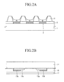
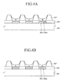
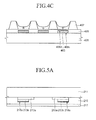
- FIG. 2A is a partial cross-sectional view showing a rear panel of a plasma display panel including carbon-containing address electrodes 3
- FIG. 2B is a partial cross-sectional view showing a front panel of a plasma display panel including a carbon-containing bus electrode 13b.
- the invention is not limited to a metal oxide, but can include common oxides used for a dielectric substance.
- a smokeless glass powder selected from the group consisting of ZnO, B 2 O 3 , Al 2 O 3 , SiO 2 , SnO, P 2 O 5 , Sb 2 O 3 , and Bi 2 O 3 may be used.
- the metal oxide may be one or more selected from the group consisting of zinc oxide - silicon oxide (ZnO-SiO 2 ), zinc oxide - boron oxide - silicon oxide (ZnO-B 2 O 3 -SiO 2 ), zinc oxide - boron oxide - silicon oxide - aluminum oxide (ZnO-B 2 O 3 -SiO 2 -Al 2 O 3 ), bismuth oxide - silicon oxide (Bi 2 O 3 -SiO 2 ), bismuth oxide - boron oxide - silicon oxide (Bi 2 O 3 -B 2 O 3 -SiO 2 ), bismuth oxide - boron oxide - silicon oxide (Bi 2 O 3 -B 2 O 3 -SiO 2 ), bismuth oxide - boron oxide - silicon oxide (Bi 2 O 3 -B 2 O 3 -SiO 2 ), bismuth oxide - boron oxide - silicon oxide (Bi 2 O 3 -B 2 O 3 -S
Landscapes
- Engineering & Computer Science (AREA)
- Physics & Mathematics (AREA)
- Plasma & Fusion (AREA)
- Chemical & Material Sciences (AREA)
- Materials Engineering (AREA)
- Gas-Filled Discharge Tubes (AREA)
Applications Claiming Priority (1)
| Application Number | Priority Date | Filing Date | Title |
|---|---|---|---|
| KR1020050084652A KR100778436B1 (ko) | 2005-09-12 | 2005-09-12 | 플라즈마 디스플레이 패널 |
Publications (2)
| Publication Number | Publication Date |
|---|---|
| EP1763055A2 true EP1763055A2 (fr) | 2007-03-14 |
| EP1763055A3 EP1763055A3 (fr) | 2008-07-09 |
Family
ID=37401132
Family Applications (1)
| Application Number | Title | Priority Date | Filing Date |
|---|---|---|---|
| EP06119020A Withdrawn EP1763055A3 (fr) | 2005-09-12 | 2006-08-16 | Panneau d'affichage à plasma |
Country Status (3)
| Country | Link |
|---|---|
| US (1) | US7462988B2 (fr) |
| EP (1) | EP1763055A3 (fr) |
| KR (1) | KR100778436B1 (fr) |
Families Citing this family (2)
| Publication number | Priority date | Publication date | Assignee | Title |
|---|---|---|---|---|
| US7743630B2 (en) * | 2005-05-05 | 2010-06-29 | Guardian Industries Corp. | Method of making float glass with transparent conductive oxide (TCO) film integrally formed on tin bath side of glass and corresponding product |
| US8179044B2 (en) * | 2010-02-02 | 2012-05-15 | Samsung Sdi Co., Ltd. | Plasma display device and fabricating method for the same |
Citations (2)
| Publication number | Priority date | Publication date | Assignee | Title |
|---|---|---|---|---|
| EP1353355A1 (fr) | 2002-04-12 | 2003-10-15 | Samsung SDI Co. Ltd. | Panneau d'affichage à plasma utilisant des nanotubes de carbone et méthode pour la production d'une plaque frontale d'un panneau d'affichage à plasma |
| US20050212430A1 (en) * | 2003-11-29 | 2005-09-29 | Jeong-Chull Ahn | Plasma display panel |
Family Cites Families (14)
| Publication number | Priority date | Publication date | Assignee | Title |
|---|---|---|---|---|
| KR19990058458A (ko) * | 1997-12-30 | 1999-07-15 | 김영환 | 플라즈마 디스플레이 패널 |
| KR20010039031A (ko) * | 1999-10-28 | 2001-05-15 | 김영남 | 플라즈마 표시패널 |
| US6657396B2 (en) * | 2000-01-11 | 2003-12-02 | Sony Corporation | Alternating current driven type plasma display device and method for production thereof |
| JP2001234163A (ja) * | 2000-02-25 | 2001-08-28 | Sony Corp | 発光性結晶粒子、発光性結晶粒子組成物、表示用パネル及び平面型表示装置 |
| KR100370738B1 (ko) * | 2000-12-29 | 2003-02-05 | 엘지전자 주식회사 | 플라즈마 디스플레이 패널 |
| CN1500282A (zh) * | 2001-02-06 | 2004-05-26 | ���µ�����ҵ��ʽ���� | 等离子体显示板及其制造方法 |
| US6610354B2 (en) * | 2001-06-18 | 2003-08-26 | Applied Materials, Inc. | Plasma display panel with a low k dielectric layer |
| KR100580683B1 (ko) * | 2002-12-20 | 2006-05-15 | 엘지전자 주식회사 | 플라즈마 디스플레이 패널 |
| US7420322B2 (en) * | 2003-06-27 | 2008-09-02 | Casio Computer Co., Ltd. | Display device including a flat panel display panel |
| KR100499038B1 (ko) * | 2003-07-08 | 2005-07-01 | 엘지전자 주식회사 | 플라즈마 디스플레이 패널 |
| CN1327514C (zh) * | 2003-10-01 | 2007-07-18 | 松下电器产业株式会社 | 配线衬底及其制造方法 |
| KR20050045513A (ko) * | 2003-11-11 | 2005-05-17 | 삼성에스디아이 주식회사 | 플라즈마 디스플레이 패널 |
| KR20050082363A (ko) * | 2004-02-18 | 2005-08-23 | 엘지전자 주식회사 | 플라즈마 디스플레이 패널 소자 |
| KR100669396B1 (ko) * | 2004-05-28 | 2007-01-15 | 삼성에스디아이 주식회사 | 플라즈마 디스플레이 패널 및 그 제조방법 |
-
2005
- 2005-09-12 KR KR1020050084652A patent/KR100778436B1/ko not_active Expired - Fee Related
-
2006
- 2006-08-16 EP EP06119020A patent/EP1763055A3/fr not_active Withdrawn
- 2006-08-29 US US11/512,650 patent/US7462988B2/en not_active Expired - Fee Related
Patent Citations (2)
| Publication number | Priority date | Publication date | Assignee | Title |
|---|---|---|---|---|
| EP1353355A1 (fr) | 2002-04-12 | 2003-10-15 | Samsung SDI Co. Ltd. | Panneau d'affichage à plasma utilisant des nanotubes de carbone et méthode pour la production d'une plaque frontale d'un panneau d'affichage à plasma |
| US20050212430A1 (en) * | 2003-11-29 | 2005-09-29 | Jeong-Chull Ahn | Plasma display panel |
Also Published As
| Publication number | Publication date |
|---|---|
| EP1763055A3 (fr) | 2008-07-09 |
| US20070057636A1 (en) | 2007-03-15 |
| KR100778436B1 (ko) | 2007-11-21 |
| US7462988B2 (en) | 2008-12-09 |
| KR20070029966A (ko) | 2007-03-15 |
Similar Documents
| Publication | Publication Date | Title |
|---|---|---|
| KR100920545B1 (ko) | 플라즈마 디스플레이 패널 | |
| KR100927611B1 (ko) | 감광성 페이스트 조성물, 이를 이용하여 제조된 pdp전극, 및 이를 포함하는 pdp | |
| KR100781326B1 (ko) | 전극 형성용 페이스트 조성물 및 이를 이용하여 제조된전극을 포함하는 플라즈마 디스플레이 패널 | |
| KR20000005579A (ko) | 플라즈마디스플레이패널및그제조방법 | |
| JP3740244B2 (ja) | 導電性焼成体およびそれを用いるガス放電表示パネル | |
| EP1763055A2 (fr) | Panneau d'affichage à plasma | |
| KR100929477B1 (ko) | 플라즈마 디스플레이 패널 | |
| KR100923741B1 (ko) | 실리콘계 계면활성제를 포함하는 전극 형성용 페이스트조성물 | |
| KR100920858B1 (ko) | 플라즈마 디스플레이 패널 | |
| JP4385480B2 (ja) | プラズマディスプレイパネル用部材およびそれを用いたプラズマディスプレイパネル。 | |
| KR100739061B1 (ko) | 전극 형성용 감광성 조성물, 전사필름, 전극 및 이를포함하는 플라즈마 디스플레이 패널 | |
| JPH11109888A (ja) | 積層電極 | |
| WO2007094239A1 (fr) | Ecran plasma | |
| US7471042B2 (en) | Plasma display panel with an improved electrode | |
| JP5092650B2 (ja) | 黒色ペースト組成物及び該組成物を用いた黒色膜の製造方法 | |
| JP2002367518A (ja) | プラズマディスプレイパネル用電極、プラズマディスプレイパネル | |
| US8587198B2 (en) | Rear panel for a display device and display device including the same | |
| JP2007128859A (ja) | プラズマディスプレイパネル | |
| JP4508282B2 (ja) | プラズマディスプレイパネル | |
| JP4186504B2 (ja) | プラズマディスプレイパネル | |
| KR100978808B1 (ko) | 2층 구조를 가지는 플라즈마 디스플레이 패널용 전극 | |
| CN101111919B (zh) | 等离子显示面板 | |
| JP2002313241A (ja) | プラズマディスプレイパネル及びその製造方法 | |
| KR20120065038A (ko) | 전극 형성용 조성물 및 이로부터 형성된 전극을 포함하는 플라즈마 디스플레이 패널 | |
| JPH10104419A (ja) | カラーフィルタおよびその製造方法 |
Legal Events
| Date | Code | Title | Description |
|---|---|---|---|
| PUAI | Public reference made under article 153(3) epc to a published international application that has entered the european phase |
Free format text: ORIGINAL CODE: 0009012 |
|
| 17P | Request for examination filed |
Effective date: 20060816 |
|
| AK | Designated contracting states |
Kind code of ref document: A2 Designated state(s): AT BE BG CH CY CZ DE DK EE ES FI FR GB GR HU IE IS IT LI LT LU LV MC NL PL PT RO SE SI SK TR |
|
| AX | Request for extension of the european patent |
Extension state: AL BA HR MK YU |
|
| PUAL | Search report despatched |
Free format text: ORIGINAL CODE: 0009013 |
|
| AK | Designated contracting states |
Kind code of ref document: A3 Designated state(s): AT BE BG CH CY CZ DE DK EE ES FI FR GB GR HU IE IS IT LI LT LU LV MC NL PL PT RO SE SI SK TR |
|
| AX | Request for extension of the european patent |
Extension state: AL BA HR MK RS |
|
| AKX | Designation fees paid |
Designated state(s): DE FR GB |
|
| RAP1 | Party data changed (applicant data changed or rights of an application transferred) |
Owner name: SAMSUNG SDI CO., LTD. |
|
| 17Q | First examination report despatched |
Effective date: 20091218 |
|
| STAA | Information on the status of an ep patent application or granted ep patent |
Free format text: STATUS: THE APPLICATION IS DEEMED TO BE WITHDRAWN |
|
| 18D | Application deemed to be withdrawn |
Effective date: 20140415 |