EP1763069A1 - Halbleiterheterostruktur und deren Herstellungsverfahren - Google Patents
Halbleiterheterostruktur und deren Herstellungsverfahren Download PDFInfo
- Publication number
- EP1763069A1 EP1763069A1 EP05291841A EP05291841A EP1763069A1 EP 1763069 A1 EP1763069 A1 EP 1763069A1 EP 05291841 A EP05291841 A EP 05291841A EP 05291841 A EP05291841 A EP 05291841A EP 1763069 A1 EP1763069 A1 EP 1763069A1
- Authority
- EP
- European Patent Office
- Prior art keywords
- layer
- semiconductor heterostructure
- silicon
- additional
- buffer layer
- Prior art date
- Legal status (The legal status is an assumption and is not a legal conclusion. Google has not performed a legal analysis and makes no representation as to the accuracy of the status listed.)
- Granted
Links
Images

Classifications
-
- H—ELECTRICITY
- H10—SEMICONDUCTOR DEVICES; ELECTRIC SOLID-STATE DEVICES NOT OTHERWISE PROVIDED FOR
- H10D—INORGANIC ELECTRIC SEMICONDUCTOR DEVICES
- H10D62/00—Semiconductor bodies, or regions thereof, of devices having potential barriers
- H10D62/80—Semiconductor bodies, or regions thereof, of devices having potential barriers characterised by the materials
- H10D62/83—Semiconductor bodies, or regions thereof, of devices having potential barriers characterised by the materials being Group IV materials, e.g. B-doped Si or undoped Ge
- H10D62/832—Semiconductor bodies, or regions thereof, of devices having potential barriers characterised by the materials being Group IV materials, e.g. B-doped Si or undoped Ge being Group IV materials comprising two or more elements, e.g. SiGe
-
- H—ELECTRICITY
- H10—SEMICONDUCTOR DEVICES; ELECTRIC SOLID-STATE DEVICES NOT OTHERWISE PROVIDED FOR
- H10P—GENERIC PROCESSES OR APPARATUS FOR THE MANUFACTURE OR TREATMENT OF DEVICES COVERED BY CLASS H10
- H10P90/00—Preparation of wafers not covered by a single main group of this subclass, e.g. wafer reinforcement
- H10P90/19—Preparing inhomogeneous wafers
- H10P90/1904—Preparing vertically inhomogeneous wafers
- H10P90/1906—Preparing SOI wafers
- H10P90/1914—Preparing SOI wafers using bonding
- H10P90/1916—Preparing SOI wafers using bonding with separation or delamination along an ion implanted layer, e.g. Smart-cut
-
- H—ELECTRICITY
- H10—SEMICONDUCTOR DEVICES; ELECTRIC SOLID-STATE DEVICES NOT OTHERWISE PROVIDED FOR
- H10D—INORGANIC ELECTRIC SEMICONDUCTOR DEVICES
- H10D62/00—Semiconductor bodies, or regions thereof, of devices having potential barriers
- H10D62/80—Semiconductor bodies, or regions thereof, of devices having potential barriers characterised by the materials
- H10D62/82—Heterojunctions
- H10D62/824—Heterojunctions comprising only Group III-V materials heterojunctions, e.g. GaN/AlGaN heterojunctions
-
- H—ELECTRICITY
- H10—SEMICONDUCTOR DEVICES; ELECTRIC SOLID-STATE DEVICES NOT OTHERWISE PROVIDED FOR
- H10D—INORGANIC ELECTRIC SEMICONDUCTOR DEVICES
- H10D62/00—Semiconductor bodies, or regions thereof, of devices having potential barriers
- H10D62/80—Semiconductor bodies, or regions thereof, of devices having potential barriers characterised by the materials
- H10D62/82—Heterojunctions
- H10D62/826—Heterojunctions comprising only Group II-VI materials heterojunctions, e.g. CdTe/HgTe heterojunctions
-
- H—ELECTRICITY
- H10—SEMICONDUCTOR DEVICES; ELECTRIC SOLID-STATE DEVICES NOT OTHERWISE PROVIDED FOR
- H10P—GENERIC PROCESSES OR APPARATUS FOR THE MANUFACTURE OR TREATMENT OF DEVICES COVERED BY CLASS H10
- H10P14/00—Formation of materials, e.g. in the shape of layers or pillars
- H10P14/20—Formation of materials, e.g. in the shape of layers or pillars of semiconductor materials
- H10P14/24—Formation of materials, e.g. in the shape of layers or pillars of semiconductor materials using chemical vapour deposition [CVD]
-
- H—ELECTRICITY
- H10—SEMICONDUCTOR DEVICES; ELECTRIC SOLID-STATE DEVICES NOT OTHERWISE PROVIDED FOR
- H10P—GENERIC PROCESSES OR APPARATUS FOR THE MANUFACTURE OR TREATMENT OF DEVICES COVERED BY CLASS H10
- H10P14/00—Formation of materials, e.g. in the shape of layers or pillars
- H10P14/20—Formation of materials, e.g. in the shape of layers or pillars of semiconductor materials
- H10P14/29—Formation of materials, e.g. in the shape of layers or pillars of semiconductor materials characterised by the substrates
- H10P14/2901—Materials
- H10P14/2902—Materials being Group IVA materials
- H10P14/2905—Silicon, silicon germanium or germanium
-
- H—ELECTRICITY
- H10—SEMICONDUCTOR DEVICES; ELECTRIC SOLID-STATE DEVICES NOT OTHERWISE PROVIDED FOR
- H10P—GENERIC PROCESSES OR APPARATUS FOR THE MANUFACTURE OR TREATMENT OF DEVICES COVERED BY CLASS H10
- H10P14/00—Formation of materials, e.g. in the shape of layers or pillars
- H10P14/20—Formation of materials, e.g. in the shape of layers or pillars of semiconductor materials
- H10P14/32—Formation of materials, e.g. in the shape of layers or pillars of semiconductor materials characterised by intermediate layers between substrates and deposited layers
- H10P14/3202—Materials thereof
- H10P14/3204—Materials thereof being Group IVA semiconducting materials
- H10P14/3211—Silicon, silicon germanium or germanium
-
- H—ELECTRICITY
- H10—SEMICONDUCTOR DEVICES; ELECTRIC SOLID-STATE DEVICES NOT OTHERWISE PROVIDED FOR
- H10P—GENERIC PROCESSES OR APPARATUS FOR THE MANUFACTURE OR TREATMENT OF DEVICES COVERED BY CLASS H10
- H10P14/00—Formation of materials, e.g. in the shape of layers or pillars
- H10P14/20—Formation of materials, e.g. in the shape of layers or pillars of semiconductor materials
- H10P14/32—Formation of materials, e.g. in the shape of layers or pillars of semiconductor materials characterised by intermediate layers between substrates and deposited layers
- H10P14/3242—Structure
-
- H—ELECTRICITY
- H10—SEMICONDUCTOR DEVICES; ELECTRIC SOLID-STATE DEVICES NOT OTHERWISE PROVIDED FOR
- H10P—GENERIC PROCESSES OR APPARATUS FOR THE MANUFACTURE OR TREATMENT OF DEVICES COVERED BY CLASS H10
- H10P14/00—Formation of materials, e.g. in the shape of layers or pillars
- H10P14/20—Formation of materials, e.g. in the shape of layers or pillars of semiconductor materials
- H10P14/32—Formation of materials, e.g. in the shape of layers or pillars of semiconductor materials characterised by intermediate layers between substrates and deposited layers
- H10P14/3242—Structure
- H10P14/3244—Layer structure
- H10P14/3248—Layer structure consisting of two layers
-
- H—ELECTRICITY
- H10—SEMICONDUCTOR DEVICES; ELECTRIC SOLID-STATE DEVICES NOT OTHERWISE PROVIDED FOR
- H10P—GENERIC PROCESSES OR APPARATUS FOR THE MANUFACTURE OR TREATMENT OF DEVICES COVERED BY CLASS H10
- H10P14/00—Formation of materials, e.g. in the shape of layers or pillars
- H10P14/20—Formation of materials, e.g. in the shape of layers or pillars of semiconductor materials
- H10P14/32—Formation of materials, e.g. in the shape of layers or pillars of semiconductor materials characterised by intermediate layers between substrates and deposited layers
- H10P14/3242—Structure
- H10P14/3244—Layer structure
- H10P14/3254—Graded layers
-
- H—ELECTRICITY
- H10—SEMICONDUCTOR DEVICES; ELECTRIC SOLID-STATE DEVICES NOT OTHERWISE PROVIDED FOR
- H10P—GENERIC PROCESSES OR APPARATUS FOR THE MANUFACTURE OR TREATMENT OF DEVICES COVERED BY CLASS H10
- H10P14/00—Formation of materials, e.g. in the shape of layers or pillars
- H10P14/20—Formation of materials, e.g. in the shape of layers or pillars of semiconductor materials
- H10P14/34—Deposited materials, e.g. layers
- H10P14/3402—Deposited materials, e.g. layers characterised by the chemical composition
- H10P14/3404—Deposited materials, e.g. layers characterised by the chemical composition being Group IVA materials
-
- H—ELECTRICITY
- H10—SEMICONDUCTOR DEVICES; ELECTRIC SOLID-STATE DEVICES NOT OTHERWISE PROVIDED FOR
- H10P—GENERIC PROCESSES OR APPARATUS FOR THE MANUFACTURE OR TREATMENT OF DEVICES COVERED BY CLASS H10
- H10P14/00—Formation of materials, e.g. in the shape of layers or pillars
- H10P14/20—Formation of materials, e.g. in the shape of layers or pillars of semiconductor materials
- H10P14/34—Deposited materials, e.g. layers
- H10P14/3402—Deposited materials, e.g. layers characterised by the chemical composition
- H10P14/3404—Deposited materials, e.g. layers characterised by the chemical composition being Group IVA materials
- H10P14/3411—Silicon, silicon germanium or germanium
-
- H—ELECTRICITY
- H10—SEMICONDUCTOR DEVICES; ELECTRIC SOLID-STATE DEVICES NOT OTHERWISE PROVIDED FOR
- H10P—GENERIC PROCESSES OR APPARATUS FOR THE MANUFACTURE OR TREATMENT OF DEVICES COVERED BY CLASS H10
- H10P14/00—Formation of materials, e.g. in the shape of layers or pillars
- H10P14/20—Formation of materials, e.g. in the shape of layers or pillars of semiconductor materials
- H10P14/34—Deposited materials, e.g. layers
- H10P14/3451—Structure
-
- H—ELECTRICITY
- H10—SEMICONDUCTOR DEVICES; ELECTRIC SOLID-STATE DEVICES NOT OTHERWISE PROVIDED FOR
- H10W—GENERIC PACKAGES, INTERCONNECTIONS, CONNECTORS OR OTHER CONSTRUCTIONAL DETAILS OF DEVICES COVERED BY CLASS H10
- H10W10/00—Isolation regions in semiconductor bodies between components of integrated devices
- H10W10/10—Isolation regions comprising dielectric materials
- H10W10/181—Semiconductor-on-insulator [SOI] isolation regions, e.g. buried oxide regions of SOI wafers
Definitions
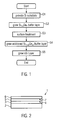
- Fig. 1 is a block diagram illustrating a first embodiment of the inventive method for forming a semiconductor heterostructure.
- a silicon substrate is provided. Silicon substrates are readily available with different sizes and different crystalline surfaces.
- a buffer layer of Si 1-x Ge x is grown, preferably epitaxially, on the silicon substrate.
- the buffer layer can be a graded buffer layer, thus the concentration of the two compounds: silicon and germanium changes over the thickness of the buffer layer.
- the germanium concentration can grow until approximately 20%, thereby the in-plane lattice parameter becomes larger. It should be noted, however, that the final germanium concentration can be freely chosen, for instance 30% or 40%, and could even reach 100%.
- the deposition could be carried out by molecular beam epitaxy.
- Table 2 Si precursor Ge precursor deposition temperature SiH 4 GeH 4 800°C - 900°C SiH 2 Cl 2 GeH 4 800°C - 950°C SiH 2 Cl 2 GeCl 4 1000°C-1100°C SiHCl 3 GeCl 4 1050°C-1150°C
- a strained silicon (sSi) layer is epitaxially deposited on the additional buffer layer using state of the art layer deposition methods.
- a second embodiment of the inventive method for forming a semiconductor heterostructure comprises steps S1 to S3 and S5 of the first embodiment. Their description will not repeated again, but is incorporated herewith by reference.
- the difference with respect to the first embodiment lies in the fact that during the growth of the additional layer (step S4) a growth temperature is used which is lower than the growth temperature used during formation of the buffer layer 3.
- the growth temperature for the additional Si 1-x Ge x layer is chosen to be about 50°C to about 500°C lower than the growth temperature of the graded buffer layer.
Landscapes
- Recrystallisation Techniques (AREA)
- Led Devices (AREA)
- Chemical Vapour Deposition (AREA)
- Element Separation (AREA)
Priority Applications (9)
| Application Number | Priority Date | Filing Date | Title |
|---|---|---|---|
| EP05291841.4A EP1763069B1 (de) | 2005-09-07 | 2005-09-07 | Herstellungsverfahren einer Heterostruktur |
| US11/267,494 US7772127B2 (en) | 2005-09-07 | 2005-11-03 | Semiconductor heterostructure and method for forming same |
| TW095128555A TWI343650B (en) | 2005-09-07 | 2006-08-03 | Semiconductor heterostructure and method for forming a semiconductor heterostructure |
| JP2006218649A JP4907256B2 (ja) | 2005-09-07 | 2006-08-10 | 半導体ヘテロ構造、および半導体ヘテロ構造を形成する方法 |
| SG200605904-2A SG131023A1 (en) | 2005-09-07 | 2006-08-29 | Semiconductor heterostructure and method for forming a semiconductor heterostructure |
| SG200901502-5A SG150571A1 (en) | 2005-09-07 | 2006-08-29 | Semiconductor heterostructure and method for forming a semiconductor heterostructure |
| KR1020060084767A KR100832152B1 (ko) | 2005-09-07 | 2006-09-04 | 반도체 헤테로구조, 반도체 헤테로구조의 형성방법 및 반도체 헤테로구조를 포함하는 절연층 위의 스트레인층 웨이퍼 |
| CN2006101289688A CN101140864B (zh) | 2005-09-07 | 2006-09-05 | 半导体异质结构和形成半导体异质结构的方法 |
| US12/827,135 US8084784B2 (en) | 2005-09-07 | 2010-06-30 | Semiconductor heterostructure and method for forming same |
Applications Claiming Priority (1)
| Application Number | Priority Date | Filing Date | Title |
|---|---|---|---|
| EP05291841.4A EP1763069B1 (de) | 2005-09-07 | 2005-09-07 | Herstellungsverfahren einer Heterostruktur |
Publications (2)
| Publication Number | Publication Date |
|---|---|
| EP1763069A1 true EP1763069A1 (de) | 2007-03-14 |
| EP1763069B1 EP1763069B1 (de) | 2016-04-13 |
Family
ID=35130550
Family Applications (1)
| Application Number | Title | Priority Date | Filing Date |
|---|---|---|---|
| EP05291841.4A Expired - Lifetime EP1763069B1 (de) | 2005-09-07 | 2005-09-07 | Herstellungsverfahren einer Heterostruktur |
Country Status (7)
| Country | Link |
|---|---|
| US (2) | US7772127B2 (de) |
| EP (1) | EP1763069B1 (de) |
| JP (1) | JP4907256B2 (de) |
| KR (1) | KR100832152B1 (de) |
| CN (1) | CN101140864B (de) |
| SG (2) | SG131023A1 (de) |
| TW (1) | TWI343650B (de) |
Cited By (4)
| Publication number | Priority date | Publication date | Assignee | Title |
|---|---|---|---|---|
| GB2467935A (en) * | 2009-02-19 | 2010-08-25 | Iqe Silicon Compounds Ltd | A method of forming a film of GaAs and germanium materials |
| WO2011082079A1 (en) * | 2009-12-30 | 2011-07-07 | Memc Electronic Materials, Inc. | Method for the preparation of a multi-layered crystalline structure |
| KR20190098308A (ko) * | 2018-02-13 | 2019-08-22 | 삼성디스플레이 주식회사 | 박막 트랜지스터 기판의 제조 방법 |
| JP2021527954A (ja) * | 2018-06-21 | 2021-10-14 | ソイテックSoitec | 前面撮像素子及びそのような撮像素子を製造するための方法 |
Families Citing this family (21)
| Publication number | Priority date | Publication date | Assignee | Title |
|---|---|---|---|---|
| US7785995B2 (en) * | 2006-05-09 | 2010-08-31 | Asm America, Inc. | Semiconductor buffer structures |
| JP5380794B2 (ja) * | 2007-06-22 | 2014-01-08 | 富士通セミコンダクター株式会社 | 半導体装置の製造方法および半導体層の形成方法 |
| FR2918793B1 (fr) * | 2007-07-11 | 2009-10-09 | Commissariat Energie Atomique | Procede de fabrication d'un substrat semiconducteur-sur- isolant pour la microelectronique et l'optoelectronique. |
| KR100873299B1 (ko) * | 2007-08-20 | 2008-12-11 | 주식회사 실트론 | Ssoi 기판의 제조방법 |
| US7791063B2 (en) * | 2007-08-30 | 2010-09-07 | Intel Corporation | High hole mobility p-channel Ge transistor structure on Si substrate |
| CN102315246B (zh) * | 2010-06-30 | 2013-03-13 | 中国科学院上海硅酸盐研究所 | 一种弛豫SiGe虚拟衬底及其制备方法 |
| CN102122636B (zh) * | 2010-12-08 | 2013-06-19 | 中国科学院上海微系统与信息技术研究所 | 三维电阻转换存储芯片制备方法 |
| FR2972567B1 (fr) * | 2011-03-09 | 2013-03-22 | Soitec Silicon On Insulator | Méthode de formation d'une structure de ge sur iii/v sur isolant |
| CN102738327A (zh) * | 2011-04-13 | 2012-10-17 | 展晶科技(深圳)有限公司 | 半导体磊晶结构及制造方法 |
| FR2977260B1 (fr) | 2011-06-30 | 2013-07-19 | Soitec Silicon On Insulator | Procede de fabrication d'une couche epitaxiale epaisse de nitrure de gallium sur un substrat de silicium ou analogue et couche obtenue par ledit procede |
| US9127345B2 (en) | 2012-03-06 | 2015-09-08 | Asm America, Inc. | Methods for depositing an epitaxial silicon germanium layer having a germanium to silicon ratio greater than 1:1 using silylgermane and a diluent |
| US9171715B2 (en) | 2012-09-05 | 2015-10-27 | Asm Ip Holding B.V. | Atomic layer deposition of GeO2 |
| FR2995447B1 (fr) | 2012-09-07 | 2014-09-05 | Soitec Silicon On Insulator | Procede de separation d'au moins deux substrats selon une interface choisie |
| US9583363B2 (en) * | 2012-12-31 | 2017-02-28 | Sunedison Semiconductor Limited (Uen201334164H) | Processes and apparatus for preparing heterostructures with reduced strain by radial distension |
| US9218963B2 (en) | 2013-12-19 | 2015-12-22 | Asm Ip Holding B.V. | Cyclical deposition of germanium |
| US9611133B2 (en) * | 2014-09-11 | 2017-04-04 | Invensense, Inc. | Film induced interface roughening and method of producing the same |
| US9490123B2 (en) * | 2014-10-24 | 2016-11-08 | Globalfoundries Inc. | Methods of forming strained epitaxial semiconductor material(S) above a strain-relaxed buffer layer |
| US10923344B2 (en) * | 2017-10-30 | 2021-02-16 | Asm Ip Holding B.V. | Methods for forming a semiconductor structure and related semiconductor structures |
| US10355105B2 (en) | 2017-10-31 | 2019-07-16 | Taiwan Semiconductor Manufacturing Company, Ltd. | Fin field-effect transistors and methods of forming the same |
| US12305270B2 (en) | 2019-11-07 | 2025-05-20 | Oerlikon Surface Solutions Ag, Pfäffikon | Method for producing a coating |
| CN112927758B (zh) * | 2019-12-05 | 2024-06-21 | 有研工程技术研究院有限公司 | 一种快速有效的异质界面建模方法 |
Citations (6)
| Publication number | Priority date | Publication date | Assignee | Title |
|---|---|---|---|---|
| US5442205A (en) | 1991-04-24 | 1995-08-15 | At&T Corp. | Semiconductor heterostructure devices with strained semiconductor layers |
| US20030203600A1 (en) * | 2002-02-11 | 2003-10-30 | International Business Machines Corporation | Strained Si based layer made by UHV-CVD, and devices therein |
| US20030215990A1 (en) | 2002-03-14 | 2003-11-20 | Eugene Fitzgerald | Methods for fabricating strained layers on semiconductor substrates |
| EP1439570A1 (de) * | 2003-01-14 | 2004-07-21 | Interuniversitair Microelektronica Centrum ( Imec) | Spannungsrelaxierte SiGe Pufferschichten für Anordnungen mit hoher Beweglichkeit und Herstellungsverfahren |
| EP1447839A1 (de) * | 2001-08-06 | 2004-08-18 | Sumitomo Mitsubishi Silicon Corporation | Halbleitersubstrat, feldeffekttransistor und verfahren zu ihrer herstellung |
| US20050179028A1 (en) * | 2004-02-17 | 2005-08-18 | Pang-Shiu Chen | Construction of thin strain-relaxed SiGe layers and method for fabricating the same |
Family Cites Families (18)
| Publication number | Priority date | Publication date | Assignee | Title |
|---|---|---|---|---|
| JPH08264552A (ja) * | 1995-03-24 | 1996-10-11 | Toshiba Ceramics Co Ltd | シリコンウエーハの製造方法 |
| US6154475A (en) * | 1997-12-04 | 2000-11-28 | The United States Of America As Represented By The Secretary Of The Air Force | Silicon-based strain-symmetrized GE-SI quantum lasers |
| US6350993B1 (en) * | 1999-03-12 | 2002-02-26 | International Business Machines Corporation | High speed composite p-channel Si/SiGe heterostructure for field effect devices |
| JP3393602B2 (ja) * | 2000-01-13 | 2003-04-07 | 松下電器産業株式会社 | 半導体装置 |
| JP3985519B2 (ja) * | 2001-12-27 | 2007-10-03 | 株式会社Sumco | 半導体基板及び電界効果型トランジスタ並びにこれらの製造方法 |
| US6562703B1 (en) * | 2002-03-13 | 2003-05-13 | Sharp Laboratories Of America, Inc. | Molecular hydrogen implantation method for forming a relaxed silicon germanium layer with high germanium content |
| JP3719998B2 (ja) | 2002-04-01 | 2005-11-24 | 松下電器産業株式会社 | 半導体装置の製造方法 |
| KR100460201B1 (ko) * | 2002-04-08 | 2004-12-08 | 한국전자통신연구원 | SiGe/Si 이종 접합 전계 효과 트랜지스터 제조용 기판의 형성 방법 |
| JP2003347229A (ja) * | 2002-05-31 | 2003-12-05 | Renesas Technology Corp | 半導体装置の製造方法および半導体装置 |
| US6995430B2 (en) * | 2002-06-07 | 2006-02-07 | Amberwave Systems Corporation | Strained-semiconductor-on-insulator device structures |
| AU2003274922A1 (en) * | 2002-08-23 | 2004-03-11 | Amberwave Systems Corporation | Semiconductor heterostructures having reduced dislocation pile-ups and related methods |
| KR100605504B1 (ko) * | 2003-07-30 | 2006-07-28 | 삼성전자주식회사 | 저전위밀도를 갖는 에피텍셜층을 포함하는 반도체 소자 및 상기 반도체 소자의 제조방법 |
| CN100459072C (zh) * | 2004-01-16 | 2009-02-04 | 国际商业机器公司 | 具有高驰豫和低堆垛层错缺陷密度的薄sgoi晶片的制作方法 |
| US6995078B2 (en) * | 2004-01-23 | 2006-02-07 | Chartered Semiconductor Manufacturing Ltd. | Method of forming a relaxed semiconductor buffer layer on a substrate with a large lattice mismatch |
| US20050274978A1 (en) * | 2004-05-27 | 2005-12-15 | Antoniadis Dimitri A | Single metal gate material CMOS using strained si-silicon germanium heterojunction layered substrate |
| US20060151787A1 (en) | 2005-01-12 | 2006-07-13 | International Business Machines Corporation | LOW CONCENTRATION SiGe BUFFER DURING STRAINED Si GROWTH OF SSGOI MATERIAL FOR DOPANT DIFFUSION CONTROL AND DEFECT REDUCTION |
| EP1705697A1 (de) * | 2005-03-21 | 2006-09-27 | S.O.I. Tec Silicon on Insulator Technologies S.A. | Zusammensetzunsgradierte Schichtstruktur und ihre Herstellung |
| EP1933384B1 (de) * | 2006-12-15 | 2013-02-13 | Soitec | Halbleiter-Heterostruktur |
-
2005
- 2005-09-07 EP EP05291841.4A patent/EP1763069B1/de not_active Expired - Lifetime
- 2005-11-03 US US11/267,494 patent/US7772127B2/en not_active Expired - Lifetime
-
2006
- 2006-08-03 TW TW095128555A patent/TWI343650B/zh active
- 2006-08-10 JP JP2006218649A patent/JP4907256B2/ja active Active
- 2006-08-29 SG SG200605904-2A patent/SG131023A1/en unknown
- 2006-08-29 SG SG200901502-5A patent/SG150571A1/en unknown
- 2006-09-04 KR KR1020060084767A patent/KR100832152B1/ko active Active
- 2006-09-05 CN CN2006101289688A patent/CN101140864B/zh active Active
-
2010
- 2010-06-30 US US12/827,135 patent/US8084784B2/en not_active Expired - Lifetime
Patent Citations (6)
| Publication number | Priority date | Publication date | Assignee | Title |
|---|---|---|---|---|
| US5442205A (en) | 1991-04-24 | 1995-08-15 | At&T Corp. | Semiconductor heterostructure devices with strained semiconductor layers |
| EP1447839A1 (de) * | 2001-08-06 | 2004-08-18 | Sumitomo Mitsubishi Silicon Corporation | Halbleitersubstrat, feldeffekttransistor und verfahren zu ihrer herstellung |
| US20030203600A1 (en) * | 2002-02-11 | 2003-10-30 | International Business Machines Corporation | Strained Si based layer made by UHV-CVD, and devices therein |
| US20030215990A1 (en) | 2002-03-14 | 2003-11-20 | Eugene Fitzgerald | Methods for fabricating strained layers on semiconductor substrates |
| EP1439570A1 (de) * | 2003-01-14 | 2004-07-21 | Interuniversitair Microelektronica Centrum ( Imec) | Spannungsrelaxierte SiGe Pufferschichten für Anordnungen mit hoher Beweglichkeit und Herstellungsverfahren |
| US20050179028A1 (en) * | 2004-02-17 | 2005-08-18 | Pang-Shiu Chen | Construction of thin strain-relaxed SiGe layers and method for fabricating the same |
Cited By (7)
| Publication number | Priority date | Publication date | Assignee | Title |
|---|---|---|---|---|
| GB2467935A (en) * | 2009-02-19 | 2010-08-25 | Iqe Silicon Compounds Ltd | A method of forming a film of GaAs and germanium materials |
| GB2467935B (en) * | 2009-02-19 | 2013-10-30 | Iqe Silicon Compounds Ltd | Formation of thin layers of GaAs and germanium materials |
| US9048289B2 (en) | 2009-02-19 | 2015-06-02 | Iqe Silicon Compounds Limited | Formation of thin layers of semiconductor materials |
| WO2011082079A1 (en) * | 2009-12-30 | 2011-07-07 | Memc Electronic Materials, Inc. | Method for the preparation of a multi-layered crystalline structure |
| US8367519B2 (en) | 2009-12-30 | 2013-02-05 | Memc Electronic Materials, Inc. | Method for the preparation of a multi-layered crystalline structure |
| KR20190098308A (ko) * | 2018-02-13 | 2019-08-22 | 삼성디스플레이 주식회사 | 박막 트랜지스터 기판의 제조 방법 |
| JP2021527954A (ja) * | 2018-06-21 | 2021-10-14 | ソイテックSoitec | 前面撮像素子及びそのような撮像素子を製造するための方法 |
Also Published As
| Publication number | Publication date |
|---|---|
| TWI343650B (en) | 2011-06-11 |
| US7772127B2 (en) | 2010-08-10 |
| TW200735348A (en) | 2007-09-16 |
| EP1763069B1 (de) | 2016-04-13 |
| US8084784B2 (en) | 2011-12-27 |
| KR20070028234A (ko) | 2007-03-12 |
| US20100264463A1 (en) | 2010-10-21 |
| KR100832152B1 (ko) | 2008-05-27 |
| CN101140864A (zh) | 2008-03-12 |
| US20070051975A1 (en) | 2007-03-08 |
| SG150571A1 (en) | 2009-03-30 |
| CN101140864B (zh) | 2011-03-02 |
| JP4907256B2 (ja) | 2012-03-28 |
| SG131023A1 (en) | 2007-04-26 |
| JP2007096274A (ja) | 2007-04-12 |
Similar Documents
| Publication | Publication Date | Title |
|---|---|---|
| US8084784B2 (en) | Semiconductor heterostructure and method for forming same | |
| US7459374B2 (en) | Method of manufacturing a semiconductor heterostructure | |
| US7544976B2 (en) | Semiconductor heterostructure | |
| EP1482549B1 (de) | Verfahren zur Herstellung einer heteroepitaktischen Mikrostruktur | |
| EP1709671B1 (de) | Verfahren zur erzeugung von dünnen sgoi-wafern mit hoher relaxations- und niedriger stapelfehlerdefektdichte | |
| US6927147B2 (en) | Coplanar integration of lattice-mismatched semiconductor with silicon via wafer bonding virtual substrates | |
| JP2008141206A6 (ja) | 半導体ヘテロ構造を作製する方法 | |
| EP1509949B1 (de) | Ausbildung von gitterabstimmungs-halbleitersubstraten | |
| JP6737983B2 (ja) | 応力を緩和するアモルファスSiO2中間層 | |
| US20070134901A1 (en) | Growth of GaAs expitaxial layers on Si substrate by using a novel GeSi buffer layer | |
| KR100611108B1 (ko) | 박막 형성 방법 |
Legal Events
| Date | Code | Title | Description |
|---|---|---|---|
| PUAI | Public reference made under article 153(3) epc to a published international application that has entered the european phase |
Free format text: ORIGINAL CODE: 0009012 |
|
| 17P | Request for examination filed |
Effective date: 20060921 |
|
| AK | Designated contracting states |
Kind code of ref document: A1 Designated state(s): AT BE BG CH CY CZ DE DK EE ES FI FR GB GR HU IE IS IT LI LT LU LV MC NL PL PT RO SE SI SK TR |
|
| AX | Request for extension of the european patent |
Extension state: AL BA HR MK YU |
|
| RIN1 | Information on inventor provided before grant (corrected) |
Inventor name: FIGUET, CHRISTOPHE Inventor name: KENNARD |
|
| AKX | Designation fees paid |
Designated state(s): AT BE BG CH CY CZ DE DK EE ES FI FR GB GR HU IE IS IT LI LT LU LV MC NL PL PT RO SE SI SK TR |
|
| 17Q | First examination report despatched |
Effective date: 20090612 |
|
| RAP1 | Party data changed (applicant data changed or rights of an application transferred) |
Owner name: SOITEC |
|
| GRAP | Despatch of communication of intention to grant a patent |
Free format text: ORIGINAL CODE: EPIDOSNIGR1 |
|
| INTG | Intention to grant announced |
Effective date: 20151120 |
|
| RIN1 | Information on inventor provided before grant (corrected) |
Inventor name: FIGUET, CHRISTOPHE Inventor name: KENNARD, MARK |
|
| GRAS | Grant fee paid |
Free format text: ORIGINAL CODE: EPIDOSNIGR3 |
|
| GRAA | (expected) grant |
Free format text: ORIGINAL CODE: 0009210 |
|
| AK | Designated contracting states |
Kind code of ref document: B1 Designated state(s): AT BE BG CH CY CZ DE DK EE ES FI FR GB GR HU IE IS IT LI LT LU LV MC NL PL PT RO SE SI SK TR |
|
| REG | Reference to a national code |
Ref country code: GB Ref legal event code: FG4D |
|
| REG | Reference to a national code |
Ref country code: AT Ref legal event code: REF Ref document number: 790955 Country of ref document: AT Kind code of ref document: T Effective date: 20160415 Ref country code: CH Ref legal event code: EP |
|
| REG | Reference to a national code |
Ref country code: IE Ref legal event code: FG4D |
|
| REG | Reference to a national code |
Ref country code: DE Ref legal event code: R096 Ref document number: 602005048944 Country of ref document: DE |
|
| REG | Reference to a national code |
Ref country code: LT Ref legal event code: MG4D |
|
| REG | Reference to a national code |
Ref country code: FR Ref legal event code: PLFP Year of fee payment: 12 |
|
| REG | Reference to a national code |
Ref country code: AT Ref legal event code: MK05 Ref document number: 790955 Country of ref document: AT Kind code of ref document: T Effective date: 20160413 |
|
| REG | Reference to a national code |
Ref country code: NL Ref legal event code: MP Effective date: 20160413 |
|
| PG25 | Lapsed in a contracting state [announced via postgrant information from national office to epo] |
Ref country code: PL Free format text: LAPSE BECAUSE OF FAILURE TO SUBMIT A TRANSLATION OF THE DESCRIPTION OR TO PAY THE FEE WITHIN THE PRESCRIBED TIME-LIMIT Effective date: 20160413 Ref country code: NL Free format text: LAPSE BECAUSE OF FAILURE TO SUBMIT A TRANSLATION OF THE DESCRIPTION OR TO PAY THE FEE WITHIN THE PRESCRIBED TIME-LIMIT Effective date: 20160413 Ref country code: LT Free format text: LAPSE BECAUSE OF FAILURE TO SUBMIT A TRANSLATION OF THE DESCRIPTION OR TO PAY THE FEE WITHIN THE PRESCRIBED TIME-LIMIT Effective date: 20160413 Ref country code: FI Free format text: LAPSE BECAUSE OF FAILURE TO SUBMIT A TRANSLATION OF THE DESCRIPTION OR TO PAY THE FEE WITHIN THE PRESCRIBED TIME-LIMIT Effective date: 20160413 |
|
| PG25 | Lapsed in a contracting state [announced via postgrant information from national office to epo] |
Ref country code: SE Free format text: LAPSE BECAUSE OF FAILURE TO SUBMIT A TRANSLATION OF THE DESCRIPTION OR TO PAY THE FEE WITHIN THE PRESCRIBED TIME-LIMIT Effective date: 20160413 Ref country code: PT Free format text: LAPSE BECAUSE OF FAILURE TO SUBMIT A TRANSLATION OF THE DESCRIPTION OR TO PAY THE FEE WITHIN THE PRESCRIBED TIME-LIMIT Effective date: 20160816 Ref country code: AT Free format text: LAPSE BECAUSE OF FAILURE TO SUBMIT A TRANSLATION OF THE DESCRIPTION OR TO PAY THE FEE WITHIN THE PRESCRIBED TIME-LIMIT Effective date: 20160413 Ref country code: LV Free format text: LAPSE BECAUSE OF FAILURE TO SUBMIT A TRANSLATION OF THE DESCRIPTION OR TO PAY THE FEE WITHIN THE PRESCRIBED TIME-LIMIT Effective date: 20160413 Ref country code: GR Free format text: LAPSE BECAUSE OF FAILURE TO SUBMIT A TRANSLATION OF THE DESCRIPTION OR TO PAY THE FEE WITHIN THE PRESCRIBED TIME-LIMIT Effective date: 20160714 Ref country code: ES Free format text: LAPSE BECAUSE OF FAILURE TO SUBMIT A TRANSLATION OF THE DESCRIPTION OR TO PAY THE FEE WITHIN THE PRESCRIBED TIME-LIMIT Effective date: 20160413 |
|
| PG25 | Lapsed in a contracting state [announced via postgrant information from national office to epo] |
Ref country code: BE Free format text: LAPSE BECAUSE OF FAILURE TO SUBMIT A TRANSLATION OF THE DESCRIPTION OR TO PAY THE FEE WITHIN THE PRESCRIBED TIME-LIMIT Effective date: 20160413 Ref country code: IT Free format text: LAPSE BECAUSE OF FAILURE TO SUBMIT A TRANSLATION OF THE DESCRIPTION OR TO PAY THE FEE WITHIN THE PRESCRIBED TIME-LIMIT Effective date: 20160413 |
|
| REG | Reference to a national code |
Ref country code: DE Ref legal event code: R097 Ref document number: 602005048944 Country of ref document: DE |
|
| PG25 | Lapsed in a contracting state [announced via postgrant information from national office to epo] |
Ref country code: EE Free format text: LAPSE BECAUSE OF FAILURE TO SUBMIT A TRANSLATION OF THE DESCRIPTION OR TO PAY THE FEE WITHIN THE PRESCRIBED TIME-LIMIT Effective date: 20160413 Ref country code: SK Free format text: LAPSE BECAUSE OF FAILURE TO SUBMIT A TRANSLATION OF THE DESCRIPTION OR TO PAY THE FEE WITHIN THE PRESCRIBED TIME-LIMIT Effective date: 20160413 Ref country code: CZ Free format text: LAPSE BECAUSE OF FAILURE TO SUBMIT A TRANSLATION OF THE DESCRIPTION OR TO PAY THE FEE WITHIN THE PRESCRIBED TIME-LIMIT Effective date: 20160413 Ref country code: DK Free format text: LAPSE BECAUSE OF FAILURE TO SUBMIT A TRANSLATION OF THE DESCRIPTION OR TO PAY THE FEE WITHIN THE PRESCRIBED TIME-LIMIT Effective date: 20160413 Ref country code: RO Free format text: LAPSE BECAUSE OF FAILURE TO SUBMIT A TRANSLATION OF THE DESCRIPTION OR TO PAY THE FEE WITHIN THE PRESCRIBED TIME-LIMIT Effective date: 20160413 |
|
| PLBE | No opposition filed within time limit |
Free format text: ORIGINAL CODE: 0009261 |
|
| STAA | Information on the status of an ep patent application or granted ep patent |
Free format text: STATUS: NO OPPOSITION FILED WITHIN TIME LIMIT |
|
| 26N | No opposition filed |
Effective date: 20170116 |
|
| PG25 | Lapsed in a contracting state [announced via postgrant information from national office to epo] |
Ref country code: MC Free format text: LAPSE BECAUSE OF FAILURE TO SUBMIT A TRANSLATION OF THE DESCRIPTION OR TO PAY THE FEE WITHIN THE PRESCRIBED TIME-LIMIT Effective date: 20160413 |
|
| REG | Reference to a national code |
Ref country code: CH Ref legal event code: PL |
|
| GBPC | Gb: european patent ceased through non-payment of renewal fee |
Effective date: 20160907 |
|
| PG25 | Lapsed in a contracting state [announced via postgrant information from national office to epo] |
Ref country code: SI Free format text: LAPSE BECAUSE OF FAILURE TO SUBMIT A TRANSLATION OF THE DESCRIPTION OR TO PAY THE FEE WITHIN THE PRESCRIBED TIME-LIMIT Effective date: 20160413 |
|
| REG | Reference to a national code |
Ref country code: IE Ref legal event code: MM4A |
|
| PG25 | Lapsed in a contracting state [announced via postgrant information from national office to epo] |
Ref country code: GB Free format text: LAPSE BECAUSE OF NON-PAYMENT OF DUE FEES Effective date: 20160907 Ref country code: CH Free format text: LAPSE BECAUSE OF NON-PAYMENT OF DUE FEES Effective date: 20160930 Ref country code: IE Free format text: LAPSE BECAUSE OF NON-PAYMENT OF DUE FEES Effective date: 20160907 Ref country code: LI Free format text: LAPSE BECAUSE OF NON-PAYMENT OF DUE FEES Effective date: 20160930 |
|
| REG | Reference to a national code |
Ref country code: FR Ref legal event code: PLFP Year of fee payment: 13 |
|
| PG25 | Lapsed in a contracting state [announced via postgrant information from national office to epo] |
Ref country code: LU Free format text: LAPSE BECAUSE OF NON-PAYMENT OF DUE FEES Effective date: 20160907 |
|
| PG25 | Lapsed in a contracting state [announced via postgrant information from national office to epo] |
Ref country code: HU Free format text: LAPSE BECAUSE OF FAILURE TO SUBMIT A TRANSLATION OF THE DESCRIPTION OR TO PAY THE FEE WITHIN THE PRESCRIBED TIME-LIMIT; INVALID AB INITIO Effective date: 20050907 Ref country code: CY Free format text: LAPSE BECAUSE OF FAILURE TO SUBMIT A TRANSLATION OF THE DESCRIPTION OR TO PAY THE FEE WITHIN THE PRESCRIBED TIME-LIMIT Effective date: 20160413 |
|
| PG25 | Lapsed in a contracting state [announced via postgrant information from national office to epo] |
Ref country code: TR Free format text: LAPSE BECAUSE OF FAILURE TO SUBMIT A TRANSLATION OF THE DESCRIPTION OR TO PAY THE FEE WITHIN THE PRESCRIBED TIME-LIMIT Effective date: 20160413 Ref country code: IS Free format text: LAPSE BECAUSE OF FAILURE TO SUBMIT A TRANSLATION OF THE DESCRIPTION OR TO PAY THE FEE WITHIN THE PRESCRIBED TIME-LIMIT Effective date: 20160413 |
|
| PG25 | Lapsed in a contracting state [announced via postgrant information from national office to epo] |
Ref country code: BG Free format text: LAPSE BECAUSE OF FAILURE TO SUBMIT A TRANSLATION OF THE DESCRIPTION OR TO PAY THE FEE WITHIN THE PRESCRIBED TIME-LIMIT Effective date: 20160413 |
|
| REG | Reference to a national code |
Ref country code: FR Ref legal event code: PLFP Year of fee payment: 14 |
|
| PGFP | Annual fee paid to national office [announced via postgrant information from national office to epo] |
Ref country code: DE Payment date: 20240806 Year of fee payment: 20 |
|
| PGFP | Annual fee paid to national office [announced via postgrant information from national office to epo] |
Ref country code: FR Payment date: 20240821 Year of fee payment: 20 |
|
| REG | Reference to a national code |
Ref country code: DE Ref legal event code: R071 Ref document number: 602005048944 Country of ref document: DE |