EP1447839A1 - Halbleitersubstrat, feldeffekttransistor und verfahren zu ihrer herstellung - Google Patents
Halbleitersubstrat, feldeffekttransistor und verfahren zu ihrer herstellung Download PDFInfo
- Publication number
- EP1447839A1 EP1447839A1 EP02755785A EP02755785A EP1447839A1 EP 1447839 A1 EP1447839 A1 EP 1447839A1 EP 02755785 A EP02755785 A EP 02755785A EP 02755785 A EP02755785 A EP 02755785A EP 1447839 A1 EP1447839 A1 EP 1447839A1
- Authority
- EP
- European Patent Office
- Prior art keywords
- layer
- sige layer
- semiconductor substrate
- sige
- composition ratio
- Prior art date
- Legal status (The legal status is an assumption and is not a legal conclusion. Google has not performed a legal analysis and makes no representation as to the accuracy of the status listed.)
- Granted
Links
Images




Classifications
-
- H—ELECTRICITY
- H10—SEMICONDUCTOR DEVICES; ELECTRIC SOLID-STATE DEVICES NOT OTHERWISE PROVIDED FOR
- H10D—INORGANIC ELECTRIC SEMICONDUCTOR DEVICES
- H10D30/00—Field-effect transistors [FET]
- H10D30/80—FETs having rectifying junction gate electrodes
- H10D30/801—FETs having heterojunction gate electrodes
-
- H—ELECTRICITY
- H10—SEMICONDUCTOR DEVICES; ELECTRIC SOLID-STATE DEVICES NOT OTHERWISE PROVIDED FOR
- H10P—GENERIC PROCESSES OR APPARATUS FOR THE MANUFACTURE OR TREATMENT OF DEVICES COVERED BY CLASS H10
- H10P10/00—Bonding of wafers, substrates or parts of devices
-
- H—ELECTRICITY
- H10—SEMICONDUCTOR DEVICES; ELECTRIC SOLID-STATE DEVICES NOT OTHERWISE PROVIDED FOR
- H10D—INORGANIC ELECTRIC SEMICONDUCTOR DEVICES
- H10D30/00—Field-effect transistors [FET]
- H10D30/60—Insulated-gate field-effect transistors [IGFET]
- H10D30/751—Insulated-gate field-effect transistors [IGFET] having composition variations in the channel regions
-
- H—ELECTRICITY
- H10—SEMICONDUCTOR DEVICES; ELECTRIC SOLID-STATE DEVICES NOT OTHERWISE PROVIDED FOR
- H10D—INORGANIC ELECTRIC SEMICONDUCTOR DEVICES
- H10D30/00—Field-effect transistors [FET]
- H10D30/60—Insulated-gate field-effect transistors [IGFET]
- H10D30/791—Arrangements for exerting mechanical stress on the crystal lattice of the channel regions
- H10D30/798—Arrangements for exerting mechanical stress on the crystal lattice of the channel regions being provided in or under the channel regions
-
- H—ELECTRICITY
- H10—SEMICONDUCTOR DEVICES; ELECTRIC SOLID-STATE DEVICES NOT OTHERWISE PROVIDED FOR
- H10P—GENERIC PROCESSES OR APPARATUS FOR THE MANUFACTURE OR TREATMENT OF DEVICES COVERED BY CLASS H10
- H10P14/00—Formation of materials, e.g. in the shape of layers or pillars
- H10P14/20—Formation of materials, e.g. in the shape of layers or pillars of semiconductor materials
- H10P14/29—Formation of materials, e.g. in the shape of layers or pillars of semiconductor materials characterised by the substrates
- H10P14/2901—Materials
- H10P14/2902—Materials being Group IVA materials
- H10P14/2905—Silicon, silicon germanium or germanium
-
- H—ELECTRICITY
- H10—SEMICONDUCTOR DEVICES; ELECTRIC SOLID-STATE DEVICES NOT OTHERWISE PROVIDED FOR
- H10P—GENERIC PROCESSES OR APPARATUS FOR THE MANUFACTURE OR TREATMENT OF DEVICES COVERED BY CLASS H10
- H10P14/00—Formation of materials, e.g. in the shape of layers or pillars
- H10P14/20—Formation of materials, e.g. in the shape of layers or pillars of semiconductor materials
- H10P14/32—Formation of materials, e.g. in the shape of layers or pillars of semiconductor materials characterised by intermediate layers between substrates and deposited layers
- H10P14/3202—Materials thereof
- H10P14/3204—Materials thereof being Group IVA semiconducting materials
- H10P14/3211—Silicon, silicon germanium or germanium
-
- H—ELECTRICITY
- H10—SEMICONDUCTOR DEVICES; ELECTRIC SOLID-STATE DEVICES NOT OTHERWISE PROVIDED FOR
- H10P—GENERIC PROCESSES OR APPARATUS FOR THE MANUFACTURE OR TREATMENT OF DEVICES COVERED BY CLASS H10
- H10P14/00—Formation of materials, e.g. in the shape of layers or pillars
- H10P14/20—Formation of materials, e.g. in the shape of layers or pillars of semiconductor materials
- H10P14/32—Formation of materials, e.g. in the shape of layers or pillars of semiconductor materials characterised by intermediate layers between substrates and deposited layers
- H10P14/3242—Structure
- H10P14/3244—Layer structure
- H10P14/3248—Layer structure consisting of two layers
-
- H—ELECTRICITY
- H10—SEMICONDUCTOR DEVICES; ELECTRIC SOLID-STATE DEVICES NOT OTHERWISE PROVIDED FOR
- H10P—GENERIC PROCESSES OR APPARATUS FOR THE MANUFACTURE OR TREATMENT OF DEVICES COVERED BY CLASS H10
- H10P14/00—Formation of materials, e.g. in the shape of layers or pillars
- H10P14/20—Formation of materials, e.g. in the shape of layers or pillars of semiconductor materials
- H10P14/32—Formation of materials, e.g. in the shape of layers or pillars of semiconductor materials characterised by intermediate layers between substrates and deposited layers
- H10P14/3242—Structure
- H10P14/3244—Layer structure
- H10P14/3251—Layer structure consisting of three or more layers
-
- H—ELECTRICITY
- H10—SEMICONDUCTOR DEVICES; ELECTRIC SOLID-STATE DEVICES NOT OTHERWISE PROVIDED FOR
- H10P—GENERIC PROCESSES OR APPARATUS FOR THE MANUFACTURE OR TREATMENT OF DEVICES COVERED BY CLASS H10
- H10P14/00—Formation of materials, e.g. in the shape of layers or pillars
- H10P14/20—Formation of materials, e.g. in the shape of layers or pillars of semiconductor materials
- H10P14/32—Formation of materials, e.g. in the shape of layers or pillars of semiconductor materials characterised by intermediate layers between substrates and deposited layers
- H10P14/3242—Structure
- H10P14/3244—Layer structure
- H10P14/3251—Layer structure consisting of three or more layers
- H10P14/3252—Alternating layers, e.g. superlattice
-
- H—ELECTRICITY
- H10—SEMICONDUCTOR DEVICES; ELECTRIC SOLID-STATE DEVICES NOT OTHERWISE PROVIDED FOR
- H10P—GENERIC PROCESSES OR APPARATUS FOR THE MANUFACTURE OR TREATMENT OF DEVICES COVERED BY CLASS H10
- H10P14/00—Formation of materials, e.g. in the shape of layers or pillars
- H10P14/20—Formation of materials, e.g. in the shape of layers or pillars of semiconductor materials
- H10P14/32—Formation of materials, e.g. in the shape of layers or pillars of semiconductor materials characterised by intermediate layers between substrates and deposited layers
- H10P14/3242—Structure
- H10P14/3244—Layer structure
- H10P14/3254—Graded layers
-
- H—ELECTRICITY
- H10—SEMICONDUCTOR DEVICES; ELECTRIC SOLID-STATE DEVICES NOT OTHERWISE PROVIDED FOR
- H10P—GENERIC PROCESSES OR APPARATUS FOR THE MANUFACTURE OR TREATMENT OF DEVICES COVERED BY CLASS H10
- H10P14/00—Formation of materials, e.g. in the shape of layers or pillars
- H10P14/20—Formation of materials, e.g. in the shape of layers or pillars of semiconductor materials
- H10P14/34—Deposited materials, e.g. layers
- H10P14/3402—Deposited materials, e.g. layers characterised by the chemical composition
- H10P14/3404—Deposited materials, e.g. layers characterised by the chemical composition being Group IVA materials
- H10P14/3411—Silicon, silicon germanium or germanium
-
- Y—GENERAL TAGGING OF NEW TECHNOLOGICAL DEVELOPMENTS; GENERAL TAGGING OF CROSS-SECTIONAL TECHNOLOGIES SPANNING OVER SEVERAL SECTIONS OF THE IPC; TECHNICAL SUBJECTS COVERED BY FORMER USPC CROSS-REFERENCE ART COLLECTIONS [XRACs] AND DIGESTS
- Y10—TECHNICAL SUBJECTS COVERED BY FORMER USPC
- Y10S—TECHNICAL SUBJECTS COVERED BY FORMER USPC CROSS-REFERENCE ART COLLECTIONS [XRACs] AND DIGESTS
- Y10S438/00—Semiconductor device manufacturing: process
- Y10S438/933—Germanium or silicon or Ge-Si on III-V
Definitions
- the present invention relates to a semiconductor substrate and field effect transistor used in high-speed MOSFETs and other similar devices, and manufacturing methods of the same.
- High-speed MOSFET, MODFET and HEMT have been proposed in recent years in which an epitaxially grown strained Si layer interposed with an SiGe (silicon-germanium) layer on a Si (silicon) substrate is used for the channel region.
- strained Si-FET tensile strain occurs in the Si layer due to the SiGe having a larger lattice constant than the Si, and as a result, the band structure of the Si changes, degeneration is removed and carrier mobility increases.
- speed can be increased to about 1.3 to 8 times faster than ordinary speeds.
- ordinary Si substrates can be used for the substrates and the CZ (Czochralski method) can be used for the process, high-speed CMOS can be realized with a conventional CMOS process.
- Examples of methods that have been proposed include a method that uses a buffer layer in which the composition ratio of Ge in the SiGe is changed at constant, gradual increments, a method that uses a buffer layer in which the composition ratio of Ge (Germanium) is changed in steps, a method that uses a buffer layer in which the Ge composition ratio is changed in the form of a super lattice, and a method that uses a buffer layer in which the Ge composition ratio is changed at a constant increment using an Si off-cut wafer (in, for example, US Patent No. 5,442,205, US Patent No. 5,221,413, PCT WO98/00857 and Japanese Unexamined Patent Application, First Publication No. 6-252046).
- the SiGe layer deposited using the aforementioned prior art was in a state such that the penetrating dislocation density and surface roughness did not reach the level desirable for use in device and manufacturing processes.
- the object of the present invention is to provide a semiconductor substrate, field effect transistor and manufacturing methods thereof that are capable of lowering penetrating dislocation density and surface roughness to practical levels.
- the semiconductor substrate of an aspect of the present invention is provided with an Si substrate, a first SiGe layer on the Si substrate, and a second SiGe layer on the first SiGe layer either directly or with an Si layer arranged between the second SiGe layer and the first SiGe layer; wherein, the first SiGe layer has a film thickness that is thinner than twice the critical film thickness, which is the film thickness at which dislocation occurs resulting in lattice relaxation due to increased film thickness, the Ge composition ratio of the second SiGe layer is at least lower than the intralayer maximum value of the Ge composition ratio in the first SiGe layer or in the first SiGe layer at the contact surface with the Si layer, and the second SiGe layer has an incremental composition region in which the Ge composition ratio gradually increases towards the surface at least in a portion thereof.
- the manufacturing method of a semiconductor substrate of an aspect of the present invention is a manufacturing method of a semiconductor substrate in which an SiGe layer is epitaxially grown on an Si substrate, and comprises a first layer formation step in which a first SiGe layer is epitaxially grown on the Si substrate, a second layer formation step in which a second SiGe layer is epitaxially grown on the first SiGe layer either directly or with an epitaxially grown Si layer arranged between the first SiGe layer and the second SiGe layer, in the first layer formation step, the film thickness of the first SiGe layer is set to be thinner than twice the critical film thickness, which is the film thickness at which dislocation occurs resulting in lattice relaxation due to increased film thickness, and in the second layer formation step, the Ge composition ratio of the second SiGe layer is at least lower than the intralayer maximum value of the Ge composition ratio in the first SiGe layer or in the first SiGe layer at the contact surface with the Si layer, and an incremental composition region is formed in which the Ge composition ratio
- the semiconductor substrate of an aspect of the present invention is a semiconductor substrate in which an SiGe layer is formed on an Si substrate, and is fabricated by the aforementioned semiconductor substrate manufacturing method of an aspect of the present invention.
- the semiconductor substrate of an aspect of the present invention is provided with an Si substrate, a first SiGe layer on the Si substrate, and a second SiGe layer on the first SiGe layer either directly or with an Si layer arranged between the second SiGe layer and the first SiGe layer; wherein, the first SiGe layer has a film thickness that is thinner than twice the critical film thickness, which is the film thickness at which dislocation occurs resulting in lattice relaxation due to increased film thickness, the second SiGe layer is composed by laminating multiple layers of an SiGe incremental composition layer, in which the Ge composition ratio gradually increases towards the surface, and an SiGe constant composition layer, which is arranged on an incremental composition layer at the Ge composition ratio of the upper surface of the incremental composition layer, at an alternating and continuous Ge composition ratio, and the Ge composition ratio of the lower surface of the second SiGe layer is lower than the intralayer maximum value of the Ge composition ratio in the first SiGe layer.
- the manufacturing method of a semiconductor substrate of an aspect of the present invention is a manufacturing method of a semiconductor substrate in which an SiGe layer is epitaxially grown on an Si substrate, comprising: a first layer formation step in which a first SiGe layer is epitaxially grown on the Si substrate, and a second layer formation step in which a second SiGe layer is epitaxially grown on the first SiGe layer either directly or with an epitaxially grown Si layer arranged between the first SiGe layer and the second SiGe layer, in the first layer formation step, the film thickness of the first SiGe layer is set to be thinner than twice the critical film thickness, which is the film thickness at which dislocation occurs resulting in lattice relaxation due to increased film thickness, and in the second layer formation step, a step in which an SiGe incremental composition layer, in which the Ge composition ratio is gradually increased towards the surface, is epitaxially grown, and a step in which an SiGe constant composition layer is epitaxially grown on the incremental composition layer at the final Ge
- the semiconductor substrate of an aspect of the present invention is a semiconductor substrate in which an SiGe layer is formed on an Si substrate, and is fabricated by the aforementioned semiconductor substrate manufacturing method of an aspect of the present invention.
- the film thickness of the first SiGe layer is set to be thinner than twice the critical film thickness, which is the film thickness at which dislocation occurs resulting in lattice relaxation due to increased film thickness
- the Ge composition ratio of the second SiGe layer is at least lower than the intralayer maximum value of the Ge composition ratio in the first SiGe layer or in the first SiGe layer at the contact surface with the Si layer
- the second SiGe layer has an incremental composition region in which the Ge composition ratio is gradually increased towards the surface in at least a portion thereof.
- the Ge composition ratio of the lower surface of the second SiGe layer is lower than the intralayer maximum value of the Ge composition ratio in the first SiGe layer.
- dislocation can be efficiently concentrated in the vicinity of the interface between the Si substrate and the first SiGe layer and the interface of the first SiGe layer and the second SiGe layer, thereby making it possible to reduce penetrating dislocation density and surface roughness on the surface of the second SiGe layer.
- the film thickness of the first SiGe layer can easily be set to within a film thickness at which remarkable generation of dislocation and lattice relaxation actually begin.
- the film thickness at which remarkable generation of dislocation and lattice relaxation actually begins changes according to the deposition temperature, if the film thickness is made to be less than twice the ideal critical film thickness t c theoretically determined from only the Ge composition ratio x and the lattice constant, it becomes thinner than the film thickness at which remarkable generation of dislocation and lattice relaxation actually begin, thereby allowing the effects of the present invention to be obtained.
- the Ge composition ratio x of the first SiGe layer is preferably from 0.05 to 0.3.
- the Ge composition ratio x of the first SiGe layer is preferably from 0.05 to 0.3.
- a semiconductor substrate is preferably produced in which a strained Si layer is formed on an Si substrate with an SiGe layer in between the strained Si layer and Si substrate, and the strained Si layer is preferably grown on a second SiGe layer of the semiconductor substrate either directly or with another SiGe layer in between.
- the semiconductor substrate of an aspect of the present invention is characterized by being a semiconductor substrate in which an SiGe layer is formed on an Si substrate, and is produced according to the aforementioned semiconductor substrate manufacturing method of the present invention. Namely, since this semiconductor substrate is produced according to the aforementioned semiconductor substrate manufacturing method of the present invention, there is little penetrating dislocation of the surface and it has satisfactory surface roughness.
- the Ge composition ratio of the first SiGe layer is from 0.05 to 0.3, the film thickness at which remarkable generation of dislocation and lattice relaxation actually begins is neither too thin or too thick, and the effects of the present invention are effectively obtained with a first SiGe layer of a suitable thickness.
- the second SiGe layer is arranged directly on the first SiGe layer, and the entire layer is in the form of an incremental composition layer in which the Ge composition ratio has been gradually increased towards the surface.
- the semiconductor substrate of an aspect of the present invention is characterized by epitaxial growth of a strained Si layer on the second SiGe layer either directly or with another SiGe layer in between.
- the field effect transistor manufacturing method of an aspect of the present invention is characterized by being a field effect transistor manufacturing method in which a channel region is formed in a strained Si layer epitaxially grown on an SiGe layer, and forms the channel region in the strained Si layer of a semiconductor substrate produced according to the aforementioned semiconductor substrate manufacturing method of the present invention.
- the field effect transistor of an aspect of the present invention is characterized by being a field effect transistor in which a channel region is formed in a strained Si layer epitaxially grown on an SiGe layer, and being produced according to the field effect transistor manufacturing method of the present invention.
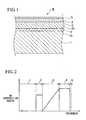
- a second SiGe layer 3 is epitaxially grown on first SiGe layer 2.
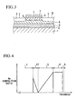
- the Ge composition ratio y of this second SiGe layer 3 is set to be at least lower than intralayer maximum value of Ge composition ratio x in the first SiGe layer 2 at the contact surface with the first SiGe layer 2.
- the second SiGe layer 3 is an incremental composition layer in which its Ge composition ratio y gradually increases towards the surface (e.g., a layer in which Ge composition ratio y increases from 0 to 0.3) (incremental composition region), and is deposited to a thickness of, for example, 1.1 ⁇ m.
- the Ge composition ratio of the second SiGe layer 3 is lower than the intralayer maximum value of the Ge composition ratio in the first SiGe layer 2 at the contact surface with the first SiGe layer 2, dislocation occurs concentrated along interfaces 2a and 2b on both sides of first SiGe layer 2, and the generation of dislocation in interfaces 2a and 2b on both sides of first SiGe layer 2 assists the lattice relaxation of second SiGe layer 3, which together with inhibiting generation of dislocation and growth within second SiGe layer 3, also inhibits worsening of surface roughness of the surface of second SiGe layer 3.
- the aforementioned deposition by vacuum CVD uses H 2 for the carrier gas and SiH 4 and GeH 4 for the source gases.
- the film thickness of the first SiGe layer 2 is set to be thinner than the film thickness at which remarkable generation of dislocation and lattice relaxation actually begin, and the Ge composition ratio y of the second SiGe layer 3 is made to at least be lower than the intralayer maximum value of Ge composition ratio x in the first SiGe layer 2 at the contact surface with the first SiGe layer 2, dislocation can be efficiently concentrated in interface 2a between Si substrate 1 and first SiGe layer 2 and interface 2b between first SiGe layer 2 and second SiGe layer 3, thereby making it possible to reduce penetrating dislocation density and surface roughness.
- the film thickness at which remarkable generation of dislocation and lattice relaxation actually begin becomes the thinnest at the same Ge composition ratio, thereby offering the advantage of a short time required for deposition since the effects of the present invention are obtained at the thinnest film thickness.
- first SiGe layer 2 have a thickness that is less than twice the critical thickness t c that satisfies the aforementioned relational expression, the film thickness of the first SiGe layer 2 can be easily set to be within the film thickness at which remarkable generation of dislocation and lattice relaxation actually begin based on experimental results to be described later.
- MOSFET field effect transistor
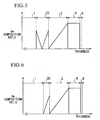
- Fig. 3 shows the schematic structure of a field effect transistor of the present invention.
- an SiO 2 gate oxide film 6 and a gate polysilicon film 7 are sequentially deposited on a strained Si layer 5 on the surface of semiconductor wafer W produced with the aforementioned manufacturing process.
- a gate electrode (not shown) is formed by patterning on gate polysilicon film 7 on the portion to serve as a channel region.
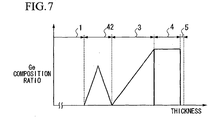
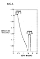
- the difference between the second embodiment and the first embodiment is that, in contrast to the Ge composition ratio being set to be constant in the first SiGe layer 2 in the first embodiment, in the second embodiment, Ge composition ratio x of a first SiGe layer 12 is made to be the intralayer maximum value at the contact surface with Si substrate 1, and Ge composition ratio x is gradually decreased as shown in Fig. 4.
- Ge composition ratio x is made to be 0.2 at the start of deposition, after which it is gradually decreased until ultimately Ge composition ratio x changes to nearly zero, resulting in an incremental composition layer that is only grown to a predetermined thickness that is thinner than the film thickness at which remarkable generation of dislocation and lattice relaxation actually begins (e.g., 350 nm).
- the Ge composition ratio x of the first SiGe layer 12 by making the Ge composition ratio x of the first SiGe layer 12 the intralayer maximum value at the contact surface with Si substrate 1, strain energy during deposition is concentrated on the side of the interface with Si substrate 1, and during lattice relaxation that occurs at the start of deposition of second SiGe layer 3, greater dislocation is generated at the interface with Si substrate 1 than at the interface with second SiGe layer 3.
- dislocation can be concentrated at a location away from the surface of second SiGe layer 3, thereby making it possible to reduce penetrating dislocation and surface roughness in the same manner as the first embodiment.
- first SiGe layer 22 is made to be in the form of a variable composition layer that is deposited to a predetermined thickness (e.g., 175 nm) by making the Ge composition ratio x at the start of deposition 0.2, and after depositing to a predetermined thickness (e.g., 175 nm) by subsequently gradually decreasing Ge composition ratio x and changing it to nearly zero, the Ge composition ratio x is then again gradually increased, finally reaching a Ge composition ratio x of 0.2.
- a predetermined thickness e.g. 175 nm
- this first SiGe layer 22 is set to be thinner than the film thickness at which remarkable generation of dislocation and lattice relaxation actually begins.
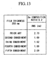
- both first SiGe layers 32 and 42 are formed at a film thickness that is thinner than the film thickness at which remarkable generation of dislocation and lattice relaxation actually begin, dislocation occurs concentrated at the interfaces on both sides of first SiGe layers 32 and 42 during deposition of second SiGe layer 3, thereby making it possible to reduce penetrating dislocation and surface roughness. Furthermore, in the fourth and fifth embodiments, since the maximum value of the Ge composition ratio in first SiGe layers 32 and 42 is not on the side of the interface with Si substrate 1, greater improvement effects on penetrating dislocation and surface roughness can be obtained than in the first and second embodiments.
- the first SiGe layer may be in the form of a multilayer film composed of a plurality of SiGe layers having different Ge composition ratios.
- the aforementioned multilayer film may also contain an Si layer.
- the first SiGe layer is only required to be a layer that contains Ge and accumulates strain energy, and other distributions of Ge composition ratios may also be employed.
- an incremental composition layer in which the Ge composition ratio is gradually increased was employed for the entire second SiGe layer in each of the aforementioned embodiments, it may also be in the form of a layer having a multilayer structure composed of incremental composition layers and uniform composition layers. In addition, it may also be in the form of a multilayer film containing an Si layer.
- the second SiGe layer was arranged directly on the first SiGe layer in each of the aforementioned embodiments, the second SiGe layer may be arranged on the first SiGe layer with an Si layer in between.
- an additional SiGe layer may be arranged on the strained Si layer of the semiconductor wafer W of each embodiment.
- a semiconductor substrate can be obtained having an SOI (silicon on insulator) structure having strained silicon, high quality and a low level of dislocation.
- a semiconductor substrate employing an SOI structure having strained silicon can be produced by the so-called smart cut method.
- the smart cut method is also referred to as the hydrogen injection delamination method, and is a method for cutting away a thin film by using a phenomenon in which a silicon single crystal lattice is partially severed as a result of injecting hydrogen ions, and particularly protons, into silicon single crystal.
- a semiconductor substrate of the present application having an SOI structure in the form of SiGe/SiO2/Si produced in this manner can be preferably used in the production of an SOI substrate like that described in, for example, US Patent No. 5,906,951.
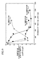
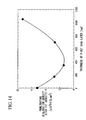
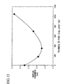
- penetrating dislocation density and surface roughness are both decreased as compared with the case of the prior art (thickness of first SiGe layer: 0) when the film thickness of the first SiGe layer is at least less than twice the critical film thickness t c .
- Fig. 1 shows the cross-sectional structure of a semiconductor wafer (semiconductor substrate) W of the present invention.
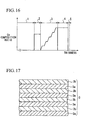
- deposition of the aforementioned second SiGe layer 3 is carried out by repeating a plurality of times at a constant Ge composition ratio a step in which an SiGe incremental composition layer 3a, in which the Ge composition ratio is gradually increased to a predetermined value towards the surface, is epitaxially grown, and a step in which an SiGe constant composition layer 3b is epitaxially grown on incremental composition layer 3a at the final Ge composition ratio of incremental composition layer 3a.
- the Ge composition ratio of the lower surface of the second SiGe layer 3 is set to be equal to or less than the Ge composite layer of the upper surface of the first SiGe layer 2.
- the Ge composition ratio of the second SiGe layer 3 is gradually increased from zero.
- a second SiGe layer 3 is formed by repeating the epitaxial growth steps of incremental composition layer 3a and constant composition layer 3b five times. Namely, when one round of epitaxial growth of incremental composition layer 3a and constant composition layer 3b is taken to be one step, the first step consists of growing a first incremental composition layer 3a on Si substrate 1 by gradually increasing the Ge composition ratio from 0 to 0.06, followed by forming a first constant composition layer 3b having a Ge composition ratio is 0.06 thereon.
- the second step consists of growing a second incremental composition layer 3a on the first constant composition layer 3b having a Ge composition ratio of 0.06 by gradually increasing the Ge composition ratio from 0.06 to 0.12, followed by forming a second constant composition layer 3b having a Ge composition ratio of 0.12 thereon.
- the third step consists of growing a third incremental composition layer 3a on the second constant composition layer 3b having a Ge composition ratio of 0.12 by gradually increasing the Ge composition ratio from 0.12 to 0.18, followed by forming a third constant composition layer 3b having a Ge composition ratio of 0.18 thereon.
- the fourth step consists of growing a fourth incremental composition layer 3a on the third constant composition layer 3b having a Ge composition ratio of 0.18 by gradually increasing the Ge composition ratio from 0.18 to 0.24, followed by forming a fourth constant composition layer 3b having a Ge composition ratio of 0.24 thereon.
- the Ge composition ratio of the second SiGe layer 3 is lower than the intralayer maximum value of the Ge composition ratio in the first SiGe layer 2 at the contact surface with the first SiGe layer 2, dislocation occurs concentrated along interfaces 2a and 2b on both sides of first SiGe layer 2, and the generation of dislocation at interfaces 2a and 2b on both sides of first SiGe layer 2 assists in lattice relaxation of second SiGe layer 3, which together with inhibiting generation of dislocation and growth within second SiGe layer 3, inhibits worsening of surface roughness of the surface of second SiGe layer 3.
- a predetermined thickness e.g. 0.75 ⁇ m
- strained Si layer 5 e.g. 20 nm
- the aforementioned deposition by vacuum CVD uses H 2 for the carrier gas and SiH 4 and GeH 4 for the source gases.
- the film thickness at which generation of dislocation and lattice relaxation actually begin becomes the thinnest at the same Ge composition ratio, thereby offering the advantage of a short time required for deposition since the effects of the present invention are obtained at the thinnest film thickness.
- first SiGe layer 2 by making first SiGe layer 2 to have a thickness that is less than twice the critical film thickness t c that satisfies the aforementioned relational expression, the film thickness of the first SiGe layer 2 can be easily set to be within the film thickness at which remarkable generation of dislocation and lattice relaxation actually begin based on experimental results to be described later.
- the first SiGe layer 2 functions as a layer that removes moisture, oxygen components, carbon components and other impurities on the surface of Si substrate 1, and is effective for inhibiting defects in Si substrate 1 caused by surface contamination.
- MOSFET field effect transistor
- Fig. 3 is a cross-sectional view showing the schematic structure of a field effect transistor of the present invention.
- an SiO 2 gate oxide film 6 and a gate polysilicon film 7 are sequentially deposited on a strained Si layer 5 on the surface of semiconductor wafer W produced with the aforementioned production process.
- a gate electrode (not shown) is formed by patterning on gate polysilicon film 7 on the portion to serve as a channel region.
- gate oxide film 6 is also patterned to remove the portion other than that beneath the gate electrode. Moreover, an n-type or p-type source region S and a drain region D are formed in a self-matching manner on strained Si layer 5 and relaxation layer 4 by ion injection using the gate electrode as a mask. Subsequently, a source electrode and drain electrode (not shown) are respectively formed on source region S and drain region D to produce an n-type or p-type MOSFET in which strained Si layer 5 serves as the channel region.
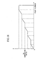
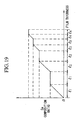
- the difference between the seventh embodiment and the sixth embodiment is that, in contrast to the film thicknesses of the incremental composition layer 3a and constant composition layer 3b in the second SiGe layer 3 in the sixth embodiment being respectively set to be the same, in the seventh embodiment, as shown in Figs. 19 and 20, the second SiGe layer 13 is formed by gradually reducing the thicknesses of incremental composition layer 13a and constant composition layer 13b for each repetition of the step in which incremental composition layer 13a and constant composition layer 13b are epitaxially grown.
- the epitaxial growth step of incremental composition layer 3a and constant composition layer 3b is repeated five times in the first embodiment
- the present embodiment differs from this in that the second SiGe layer 13 is formed by repeating the epitaxial growth step of incremental composition layer 13a and constant composition layer 13b four times.
- second incremental composition layer 13a and second constant composition layer 13b are grown to be thinner than first incremental composition layer 13a and first constant composition layer 13b.
- third incremental composition layer 13a and third constant composition layer 13b are similarly grown to be thinner than second incremental composition layer 13a and second constant composition layer 13b, and finally fourth incremental composition layer 13a and fourth constant composition layer 13b are grown to be thinner than third incremental composition layer 13a and third constant composition layer 13b to form second SiGe layer 13.
- first incremental composition layer 13a and first constant composition layer 13b are represented with l 1
- second incremental composition layer 13a and second constant composition layer 13b are represented with l 2
- third incremental composition layer 13a and third constant composition layer 13b are represented with l 3
- fourth incremental composition layer 13a and fourth constant composition layer 13b are represented with l 4
- each of the layers are laminated in the manner of l 1 ⁇ l 2 ⁇ l 3 ⁇ l 4 .
- each incremental composition layer 13a is set to be the same for each layer.
- dislocation is generated more easily the higher the Ge composition ratio, in the case of repeating deposition at the same thickness as in the sixth embodiment, in contrast to more dislocation being generated the higher the layer, by gradually reducing the thickness of incremental composition layer 13a and constant composition layer 13b for each repetition as in the present embodiment, dislocation can be made to be generated uniformly in each layer.
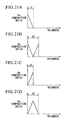
- the eighth embodiment differs from the sixth embodiment in that in contrast to the Ge composition ratio being set to be constant in the first SiGe layer 2 in the sixth embodiment, in the eighth embodiment, as shown in Figs. 21A through 21D, the Ge composition ratio x of the first SiGe layer is not constant.
- the Ge composition ratio x of the first SiGe layer 12 reaches an intralayer maximum value at the contact surface with Si substrate 1, after which the Ge composition ratio x is gradually decreased.
- the Ge composition ratio x is made to be 0.3 at the start of deposition, after which it is gradually decreased until ultimately Ge composition ratio x changes to nearly zero, resulting in an incremental composition layer that is only grown to a predetermined thickness that is thinner than the film thickness at which remarkable generation of dislocation and lattice relaxation actually begins (e.g., 350 nm).
- the Ge composition ratio x of a first SiGe layer 32 is gradually increased from nearly zero to ultimately 0.2, and deposited at a predetermined thickness (e.g., 175 nm) that is thinner than the film thickness at which remarkable generation of dislocation and lattice relaxation actually begins.
- the Ge composition ratio x of a first SiGe layer 42 is deposited at a predetermined thickness (e.g., 175 nm) while gradually increasing from nearly zero to 0.2, and then subsequently deposited at a predetermined thickness (e.g., 175 nm) while gradually decreasing Ge composition ratio x from 0.2 to nearly zero. Furthermore, the thickness of first SiGe layer 42 is set to be thinner than the film thickness at which remarkable generation of dislocation and lattice relaxation actually begin.
- both first SiGe layers 32 and 42 are formed at a film thickness that is thinner than the film thickness at which remarkable generation of dislocation and lattice relaxation actually begin, dislocation occurs concentrated at the interfaces on both sides of first SiGe layers 32 and 42 during deposition of second SiGe layer 3, thereby making it possible to reduce penetrating dislocation and surface roughness. Furthermore, in the fourth and fifth examples, since the maximum value of the Ge composition ratio in first SiGe layers 32 and 42 is not on the side of the interface with Si substrate 1, greater improvement effects on penetrating dislocation and surface roughness can be obtained than in the first and second embodiments.
- the first SiGe layer may be in the form of a multilayer film composed of a plurality of SiGe layers having different Ge composition ratios.
- the aforementioned multilayer film may also contain an Si layer.
- composition was changed at a constant ratio relative to film thickness in the case of having changed the Ge composition ratio in the first SiGe layer in each of the aforementioned embodiments, a structure may also be employed in which that ratio is not constant.
- the first SiGe layer is only required to be a layer that contains Ge and accumulates strain energy, and other distributions of Ge composition ratios may also be employed.
- composition of an incremental composition layer in which the Ge composition ratio is gradually increased towards the surface in the second SiGe layer was changed at a constant ratio versus film thickness in each of the aforementioned embodiments, a structure may also be employed in which that ratio is not constant.
- the Ge composition ratio of a second SiGe layer is at least made to be lower than the intralayer maximum value of the first SiGe layer at the contact surface with the first SiGe layer or an Si substrate, and the second SiGe layer has an incremental composition layer in which the Ge composition ratio is gradually increased towards the surface at least in a portion thereof, dislocation can be efficiently concentrated at the interface between the Si substrate and first SiGe layer and in the vicinity of the interface between the first SiGe layer and the second SiGe layer, thereby enabling penetrating dislocation density and surface roughness of the surface of the second SiGe layer to be reduced.
Landscapes
- Insulated Gate Type Field-Effect Transistor (AREA)
- Recrystallisation Techniques (AREA)
- Thin Film Transistor (AREA)
Applications Claiming Priority (5)
| Application Number | Priority Date | Filing Date | Title |
|---|---|---|---|
| JP2001238172 | 2001-08-06 | ||
| JP2001238172A JP4345249B2 (ja) | 2001-08-06 | 2001-08-06 | 半導体基板及び電界効果型トランジスタ並びにこれらの製造方法 |
| JP2001396966A JP3985519B2 (ja) | 2001-12-27 | 2001-12-27 | 半導体基板及び電界効果型トランジスタ並びにこれらの製造方法 |
| JP2001296966 | 2001-12-27 | ||
| PCT/JP2002/007903 WO2003015140A1 (en) | 2001-08-06 | 2002-08-02 | Semiconductor substrate, field-effct transistor, and their manufacturing methods |
Publications (3)
| Publication Number | Publication Date |
|---|---|
| EP1447839A1 true EP1447839A1 (de) | 2004-08-18 |
| EP1447839A4 EP1447839A4 (de) | 2009-11-04 |
| EP1447839B1 EP1447839B1 (de) | 2019-05-22 |
Family
ID=26620031
Family Applications (1)
| Application Number | Title | Priority Date | Filing Date |
|---|---|---|---|
| EP02755785.9A Expired - Lifetime EP1447839B1 (de) | 2001-08-06 | 2002-08-02 | Halbleitersubstrat, feldeffekttransistor und verfahren zu ihrer herstellung |
Country Status (5)
| Country | Link |
|---|---|
| US (1) | US7138650B2 (de) |
| EP (1) | EP1447839B1 (de) |
| KR (1) | KR100710513B1 (de) |
| TW (1) | TW580727B (de) |
| WO (1) | WO2003015140A1 (de) |
Cited By (4)
| Publication number | Priority date | Publication date | Assignee | Title |
|---|---|---|---|---|
| EP1763069A1 (de) * | 2005-09-07 | 2007-03-14 | S.O.I.TEC. Silicon on Insulator Technologies S.A. | Halbleiterheterostruktur und deren Herstellungsverfahren |
| US7459374B2 (en) | 2006-11-30 | 2008-12-02 | S.O.I.Tec Silicon On Insulator Technologies | Method of manufacturing a semiconductor heterostructure |
| EP2461352A1 (de) * | 2010-12-06 | 2012-06-06 | Imec | Verfahren zur Herstellung von Kontakten mit geringem Widerstand auf n-Germanium |
| CN105702826A (zh) * | 2014-11-25 | 2016-06-22 | 东莞市中镓半导体科技有限公司 | 一种在Si衬底上制备无裂纹GaN薄膜的方法 |
Families Citing this family (12)
| Publication number | Priority date | Publication date | Assignee | Title |
|---|---|---|---|---|
| JP2003520444A (ja) | 2000-01-20 | 2003-07-02 | アンバーウェーブ システムズ コーポレイション | 高温成長を不要とする低貫通転位密度格子不整合エピ層 |
| AU2003274922A1 (en) | 2002-08-23 | 2004-03-11 | Amberwave Systems Corporation | Semiconductor heterostructures having reduced dislocation pile-ups and related methods |
| US7594967B2 (en) | 2002-08-30 | 2009-09-29 | Amberwave Systems Corporation | Reduction of dislocation pile-up formation during relaxed lattice-mismatched epitaxy |
| US6946373B2 (en) * | 2002-11-20 | 2005-09-20 | International Business Machines Corporation | Relaxed, low-defect SGOI for strained Si CMOS applications |
| US7332417B2 (en) | 2003-01-27 | 2008-02-19 | Amberwave Systems Corporation | Semiconductor structures with structural homogeneity |
| JP4306266B2 (ja) | 2003-02-04 | 2009-07-29 | 株式会社Sumco | 半導体基板の製造方法 |
| US20080050883A1 (en) * | 2006-08-25 | 2008-02-28 | Atmel Corporation | Hetrojunction bipolar transistor (hbt) with periodic multilayer base |
| US8530934B2 (en) | 2005-11-07 | 2013-09-10 | Atmel Corporation | Integrated circuit structures containing a strain-compensated compound semiconductor layer and methods and systems related thereto |
| JP4271210B2 (ja) * | 2006-06-30 | 2009-06-03 | 株式会社東芝 | 電界効果トランジスタ、集積回路素子、及びそれらの製造方法 |
| US7550758B2 (en) | 2006-10-31 | 2009-06-23 | Atmel Corporation | Method for providing a nanoscale, high electron mobility transistor (HEMT) on insulator |
| KR101013495B1 (ko) * | 2008-08-19 | 2011-02-10 | 한양대학교 산학협력단 | 고무장갑 건조기 |
| JPWO2014103428A1 (ja) * | 2012-12-28 | 2017-01-12 | 株式会社村田製作所 | 垂直共振面発光レーザ |
Family Cites Families (15)
| Publication number | Priority date | Publication date | Assignee | Title |
|---|---|---|---|---|
| US5221413A (en) | 1991-04-24 | 1993-06-22 | At&T Bell Laboratories | Method for making low defect density semiconductor heterostructure and devices made thereby |
| US5442205A (en) * | 1991-04-24 | 1995-08-15 | At&T Corp. | Semiconductor heterostructure devices with strained semiconductor layers |
| US5534713A (en) | 1994-05-20 | 1996-07-09 | International Business Machines Corporation | Complementary metal-oxide semiconductor transistor logic using strained SI/SIGE heterostructure layers |
| JP3116731B2 (ja) * | 1994-07-25 | 2000-12-11 | 株式会社日立製作所 | 格子不整合系積層結晶構造およびそれを用いた半導体装置 |
| JPH08339193A (ja) * | 1995-06-13 | 1996-12-24 | Yamaha Corp | カラオケ装置 |
| JP3441277B2 (ja) * | 1995-12-26 | 2003-08-25 | 株式会社東芝 | 半導体装置およびその製造方法 |
| US6039803A (en) | 1996-06-28 | 2000-03-21 | Massachusetts Institute Of Technology | Utilization of miscut substrates to improve relaxed graded silicon-germanium and germanium layers on silicon |
| US5906951A (en) | 1997-04-30 | 1999-05-25 | International Business Machines Corporation | Strained Si/SiGe layers on insulator |
| US6723621B1 (en) * | 1997-06-30 | 2004-04-20 | International Business Machines Corporation | Abrupt delta-like doping in Si and SiGe films by UHV-CVD |
| JP3658745B2 (ja) * | 1998-08-19 | 2005-06-08 | 株式会社ルネサステクノロジ | バイポーラトランジスタ |
| US6369438B1 (en) * | 1998-12-24 | 2002-04-09 | Kabushiki Kaisha Toshiba | Semiconductor device and method for manufacturing the same |
| US6350993B1 (en) | 1999-03-12 | 2002-02-26 | International Business Machines Corporation | High speed composite p-channel Si/SiGe heterostructure for field effect devices |
| US6339232B1 (en) * | 1999-09-20 | 2002-01-15 | Kabushika Kaisha Toshiba | Semiconductor device |
| DE10002364A1 (de) * | 2000-01-20 | 2001-08-02 | Infineon Technologies Ag | Silizium-Germanium-Bipolartranistor mit optimiertem Germaniumprofil |
| US6555839B2 (en) * | 2000-05-26 | 2003-04-29 | Amberwave Systems Corporation | Buried channel strained silicon FET using a supply layer created through ion implantation |
-
2002
- 2002-08-02 EP EP02755785.9A patent/EP1447839B1/de not_active Expired - Lifetime
- 2002-08-02 KR KR1020047001728A patent/KR100710513B1/ko not_active Expired - Fee Related
- 2002-08-02 US US10/485,727 patent/US7138650B2/en not_active Expired - Lifetime
- 2002-08-02 WO PCT/JP2002/007903 patent/WO2003015140A1/ja not_active Ceased
- 2002-08-06 TW TW091117690A patent/TW580727B/zh not_active IP Right Cessation
Cited By (8)
| Publication number | Priority date | Publication date | Assignee | Title |
|---|---|---|---|---|
| EP1763069A1 (de) * | 2005-09-07 | 2007-03-14 | S.O.I.TEC. Silicon on Insulator Technologies S.A. | Halbleiterheterostruktur und deren Herstellungsverfahren |
| US7772127B2 (en) | 2005-09-07 | 2010-08-10 | S.O.I.Tec Silicon On Insulator Technologies | Semiconductor heterostructure and method for forming same |
| US8084784B2 (en) | 2005-09-07 | 2011-12-27 | S.O.I. Tec Silicon On Insulator Technologies | Semiconductor heterostructure and method for forming same |
| US7459374B2 (en) | 2006-11-30 | 2008-12-02 | S.O.I.Tec Silicon On Insulator Technologies | Method of manufacturing a semiconductor heterostructure |
| EP2461352A1 (de) * | 2010-12-06 | 2012-06-06 | Imec | Verfahren zur Herstellung von Kontakten mit geringem Widerstand auf n-Germanium |
| US9177812B2 (en) | 2010-12-06 | 2015-11-03 | Imec | Method of manufacturing low resistivity contacts on n-type germanium |
| CN105702826A (zh) * | 2014-11-25 | 2016-06-22 | 东莞市中镓半导体科技有限公司 | 一种在Si衬底上制备无裂纹GaN薄膜的方法 |
| CN105702826B (zh) * | 2014-11-25 | 2018-10-19 | 东莞市中镓半导体科技有限公司 | 一种在Si衬底上制备无裂纹GaN薄膜的方法 |
Also Published As
| Publication number | Publication date |
|---|---|
| EP1447839B1 (de) | 2019-05-22 |
| US7138650B2 (en) | 2006-11-21 |
| EP1447839A4 (de) | 2009-11-04 |
| US20040251458A1 (en) | 2004-12-16 |
| KR100710513B1 (ko) | 2007-04-23 |
| WO2003015140A1 (en) | 2003-02-20 |
| TW580727B (en) | 2004-03-21 |
| KR20040037060A (ko) | 2004-05-04 |
Similar Documents
| Publication | Publication Date | Title |
|---|---|---|
| EP2631933B1 (de) | Herstellungsverfahren für ein Halbleitersubstrat | |
| US6525338B2 (en) | Semiconductor substrate, field effect transistor, method of forming SiGe layer and method of forming strained Si layer using same, and method of manufacturing field effect transistor | |
| US7138650B2 (en) | Semiconductor substrate, field-effect transistor, and their manufacturing method of the same | |
| JP2014075585A (ja) | 減少した転位パイルアップを有する半導体ヘテロ構造および関連した方法 | |
| US8043929B2 (en) | Semiconductor substrate and method for production thereof | |
| EP1437765B1 (de) | Herstellungsverfahren für ein halbleitersubstrat und herstellungsverfahren für einen feldeffekttransistor | |
| KR100738766B1 (ko) | 반도체 기판의 제조 방법 및 전계 효과형 트랜지스터의 제조 방법 | |
| JP2006080278A (ja) | 歪みシリコンウエハおよびその製造方法 | |
| JP3985519B2 (ja) | 半導体基板及び電界効果型トランジスタ並びにこれらの製造方法 | |
| JP4039013B2 (ja) | 半導体基板と電界効果型トランジスタ並びにSiGe層の形成方法及びこれを用いた歪みSi層の形成方法と電界効果型トランジスタの製造方法 | |
| JP4296727B2 (ja) | 半導体基板と電界効果型トランジスタ並びにSiGe層の形成方法及びこれを用いた歪みSi層の形成方法と電界効果型トランジスタの製造方法 | |
| JP4345249B2 (ja) | 半導体基板及び電界効果型トランジスタ並びにこれらの製造方法 | |
| KR100776965B1 (ko) | 반도체 기판 및 전계 효과형 트랜지스터 및 그 제조 방법 | |
| JP4221928B2 (ja) | 半導体基板及び電界効果型トランジスタ並びにこれらの製造方法 | |
| JP4254102B2 (ja) | 半導体基板及び電界効果型トランジスタ並びにこれらの製造方法 | |
| JP2003133548A (ja) | 半導体基板及び電界効果型トランジスタ並びにこれらの製造方法 | |
| CN121793740A (zh) | 应变半导体结构、绝缘体上半导体结构及制备方法 |
Legal Events
| Date | Code | Title | Description |
|---|---|---|---|
| PUAI | Public reference made under article 153(3) epc to a published international application that has entered the european phase |
Free format text: ORIGINAL CODE: 0009012 |
|
| 17P | Request for examination filed |
Effective date: 20040204 |
|
| AK | Designated contracting states |
Kind code of ref document: A1 Designated state(s): AT BE BG CH CY CZ DE DK EE ES FI FR GB GR IE IT LI LU MC NL PT SE TR |
|
| AX | Request for extension of the european patent |
Extension state: AL LT LV MK RO SI |
|
| RAP1 | Party data changed (applicant data changed or rights of an application transferred) |
Owner name: SUMCO CORPORATION |
|
| A4 | Supplementary search report drawn up and despatched |
Effective date: 20091005 |
|
| 17Q | First examination report despatched |
Effective date: 20091211 |
|
| GRAP | Despatch of communication of intention to grant a patent |
Free format text: ORIGINAL CODE: EPIDOSNIGR1 |
|
| INTG | Intention to grant announced |
Effective date: 20190111 |
|
| RBV | Designated contracting states (corrected) |
Designated state(s): DE FR GB |
|
| RIN1 | Information on inventor provided before grant (corrected) |
Inventor name: YAMAGUCHI, KENJI, C/O MITSUBISHI SILICON CORP. Inventor name: MIZUSHIMA, KAZUKI, C/O MITSUBISHI SILICON CORP. Inventor name: SHIONO, ICHIRO, C/O MITSUBISHI SILICON CORP. |
|
| RIC1 | Information provided on ipc code assigned before grant |
Ipc: H01L 29/161 20060101ALI20030226BHEP Ipc: H01L 21/20 20060101AFI20030226BHEP Ipc: H01L 21/205 20060101ALI20030226BHEP Ipc: H01L 29/786 20060101ALI20030226BHEP Ipc: H01L 21/336 20060101ALI20030226BHEP Ipc: H01L 29/78 20060101ALI20030226BHEP |
|
| GRAS | Grant fee paid |
Free format text: ORIGINAL CODE: EPIDOSNIGR3 |
|
| GRAA | (expected) grant |
Free format text: ORIGINAL CODE: 0009210 |
|
| AK | Designated contracting states |
Kind code of ref document: B1 Designated state(s): DE FR GB |
|
| REG | Reference to a national code |
Ref country code: GB Ref legal event code: FG4D |
|
| REG | Reference to a national code |
Ref country code: DE Ref legal event code: R096 Ref document number: 60249912 Country of ref document: DE |
|
| REG | Reference to a national code |
Ref country code: DE Ref legal event code: R097 Ref document number: 60249912 Country of ref document: DE |
|
| PLBE | No opposition filed within time limit |
Free format text: ORIGINAL CODE: 0009261 |
|
| STAA | Information on the status of an ep patent application or granted ep patent |
Free format text: STATUS: NO OPPOSITION FILED WITHIN TIME LIMIT |
|
| 26N | No opposition filed |
Effective date: 20200225 |
|
| PGFP | Annual fee paid to national office [announced via postgrant information from national office to epo] |
Ref country code: FR Payment date: 20210819 Year of fee payment: 20 |
|
| PGFP | Annual fee paid to national office [announced via postgrant information from national office to epo] |
Ref country code: GB Payment date: 20210820 Year of fee payment: 20 Ref country code: DE Payment date: 20210819 Year of fee payment: 20 |
|
| REG | Reference to a national code |
Ref country code: DE Ref legal event code: R071 Ref document number: 60249912 Country of ref document: DE |
|
| REG | Reference to a national code |
Ref country code: GB Ref legal event code: PE20 Expiry date: 20220801 |
|
| PG25 | Lapsed in a contracting state [announced via postgrant information from national office to epo] |
Ref country code: GB Free format text: LAPSE BECAUSE OF EXPIRATION OF PROTECTION Effective date: 20220801 |