EP1763295A2 - Panneau avec des composants enterrés et méthode de fabrication associée - Google Patents
Panneau avec des composants enterrés et méthode de fabrication associée Download PDFInfo
- Publication number
- EP1763295A2 EP1763295A2 EP06019174A EP06019174A EP1763295A2 EP 1763295 A2 EP1763295 A2 EP 1763295A2 EP 06019174 A EP06019174 A EP 06019174A EP 06019174 A EP06019174 A EP 06019174A EP 1763295 A2 EP1763295 A2 EP 1763295A2
- Authority
- EP
- European Patent Office
- Prior art keywords
- substrate
- electronic component
- resin
- embedded board
- component embedded
- Prior art date
- Legal status (The legal status is an assumption and is not a legal conclusion. Google has not performed a legal analysis and makes no representation as to the accuracy of the status listed.)
- Withdrawn
Links
Images




Classifications
-
- H—ELECTRICITY
- H05—ELECTRIC TECHNIQUES NOT OTHERWISE PROVIDED FOR
- H05K—PRINTED CIRCUITS; CASINGS OR CONSTRUCTIONAL DETAILS OF ELECTRIC APPARATUS; MANUFACTURE OF ASSEMBLAGES OF ELECTRICAL COMPONENTS
- H05K1/00—Printed circuits
- H05K1/18—Printed circuits structurally associated with non-printed electric components
- H05K1/182—Printed circuits structurally associated with non-printed electric components associated with components mounted in printed circuit boards [PCB], e.g. insert-mounted components [IMC]
- H05K1/185—Printed circuits structurally associated with non-printed electric components associated with components mounted in printed circuit boards [PCB], e.g. insert-mounted components [IMC] associated with components encapsulated in the insulating substrate of the PCBs; associated with components incorporated in internal layers of multilayer circuit boards
- H05K1/186—Printed circuits structurally associated with non-printed electric components associated with components mounted in printed circuit boards [PCB], e.g. insert-mounted components [IMC] associated with components encapsulated in the insulating substrate of the PCBs; associated with components incorporated in internal layers of multilayer circuit boards manufactured by mounting on or connecting to patterned circuits before or during embedding
-
- H—ELECTRICITY
- H10—SEMICONDUCTOR DEVICES; ELECTRIC SOLID-STATE DEVICES NOT OTHERWISE PROVIDED FOR
- H10W—GENERIC PACKAGES, INTERCONNECTIONS, CONNECTORS OR OTHER CONSTRUCTIONAL DETAILS OF DEVICES COVERED BY CLASS H10
- H10W70/00—Package substrates; Interposers; Redistribution layers [RDL]
- H10W70/60—Insulating or insulated package substrates; Interposers; Redistribution layers
- H10W70/611—Insulating or insulated package substrates; Interposers; Redistribution layers for connecting multiple chips together
-
- H—ELECTRICITY
- H10—SEMICONDUCTOR DEVICES; ELECTRIC SOLID-STATE DEVICES NOT OTHERWISE PROVIDED FOR
- H10W—GENERIC PACKAGES, INTERCONNECTIONS, CONNECTORS OR OTHER CONSTRUCTIONAL DETAILS OF DEVICES COVERED BY CLASS H10
- H10W70/00—Package substrates; Interposers; Redistribution layers [RDL]
- H10W70/60—Insulating or insulated package substrates; Interposers; Redistribution layers
- H10W70/611—Insulating or insulated package substrates; Interposers; Redistribution layers for connecting multiple chips together
- H10W70/614—Insulating or insulated package substrates; Interposers; Redistribution layers for connecting multiple chips together the multiple chips being integrally enclosed
-
- H—ELECTRICITY
- H10—SEMICONDUCTOR DEVICES; ELECTRIC SOLID-STATE DEVICES NOT OTHERWISE PROVIDED FOR
- H10W—GENERIC PACKAGES, INTERCONNECTIONS, CONNECTORS OR OTHER CONSTRUCTIONAL DETAILS OF DEVICES COVERED BY CLASS H10
- H10W90/00—Package configurations
-
- H—ELECTRICITY
- H10—SEMICONDUCTOR DEVICES; ELECTRIC SOLID-STATE DEVICES NOT OTHERWISE PROVIDED FOR
- H10W—GENERIC PACKAGES, INTERCONNECTIONS, CONNECTORS OR OTHER CONSTRUCTIONAL DETAILS OF DEVICES COVERED BY CLASS H10
- H10W90/00—Package configurations
- H10W90/401—Package configurations characterised by multiple insulating or insulated package substrates, interposers or RDLs
-
- H—ELECTRICITY
- H05—ELECTRIC TECHNIQUES NOT OTHERWISE PROVIDED FOR
- H05K—PRINTED CIRCUITS; CASINGS OR CONSTRUCTIONAL DETAILS OF ELECTRIC APPARATUS; MANUFACTURE OF ASSEMBLAGES OF ELECTRICAL COMPONENTS
- H05K2201/00—Indexing scheme relating to printed circuits covered by H05K1/00
- H05K2201/01—Dielectrics
- H05K2201/0183—Dielectric layers
- H05K2201/0195—Dielectric or adhesive layers comprising a plurality of layers, e.g. in a multilayer structure
-
- H—ELECTRICITY
- H05—ELECTRIC TECHNIQUES NOT OTHERWISE PROVIDED FOR
- H05K—PRINTED CIRCUITS; CASINGS OR CONSTRUCTIONAL DETAILS OF ELECTRIC APPARATUS; MANUFACTURE OF ASSEMBLAGES OF ELECTRICAL COMPONENTS
- H05K2201/00—Indexing scheme relating to printed circuits covered by H05K1/00
- H05K2201/10—Details of components or other objects attached to or integrated in a printed circuit board
- H05K2201/10613—Details of electrical connections of non-printed components, e.g. special leads
- H05K2201/10621—Components characterised by their electrical contacts
- H05K2201/10674—Flip chip
-
- H—ELECTRICITY
- H05—ELECTRIC TECHNIQUES NOT OTHERWISE PROVIDED FOR
- H05K—PRINTED CIRCUITS; CASINGS OR CONSTRUCTIONAL DETAILS OF ELECTRIC APPARATUS; MANUFACTURE OF ASSEMBLAGES OF ELECTRICAL COMPONENTS
- H05K2203/00—Indexing scheme relating to apparatus or processes for manufacturing printed circuits covered by H05K3/00
- H05K2203/06—Lamination
- H05K2203/061—Lamination of previously made multilayered subassemblies
-
- H—ELECTRICITY
- H05—ELECTRIC TECHNIQUES NOT OTHERWISE PROVIDED FOR
- H05K—PRINTED CIRCUITS; CASINGS OR CONSTRUCTIONAL DETAILS OF ELECTRIC APPARATUS; MANUFACTURE OF ASSEMBLAGES OF ELECTRICAL COMPONENTS
- H05K3/00—Apparatus or processes for manufacturing printed circuits
- H05K3/0011—Working of insulating substrates or insulating layers
- H05K3/0017—Etching of the substrate by chemical or physical means
- H05K3/0023—Etching of the substrate by chemical or physical means by exposure and development of a photosensitive insulating layer
-
- H—ELECTRICITY
- H05—ELECTRIC TECHNIQUES NOT OTHERWISE PROVIDED FOR
- H05K—PRINTED CIRCUITS; CASINGS OR CONSTRUCTIONAL DETAILS OF ELECTRIC APPARATUS; MANUFACTURE OF ASSEMBLAGES OF ELECTRICAL COMPONENTS
- H05K3/00—Apparatus or processes for manufacturing printed circuits
- H05K3/46—Manufacturing multilayer circuits
- H05K3/4611—Manufacturing multilayer circuits by laminating two or more circuit boards
- H05K3/4614—Manufacturing multilayer circuits by laminating two or more circuit boards the electrical connections between the circuit boards being made during lamination
-
- H—ELECTRICITY
- H10—SEMICONDUCTOR DEVICES; ELECTRIC SOLID-STATE DEVICES NOT OTHERWISE PROVIDED FOR
- H10W—GENERIC PACKAGES, INTERCONNECTIONS, CONNECTORS OR OTHER CONSTRUCTIONAL DETAILS OF DEVICES COVERED BY CLASS H10
- H10W72/00—Interconnections or connectors in packages
- H10W72/071—Connecting or disconnecting
- H10W72/073—Connecting or disconnecting of die-attach connectors
-
- H—ELECTRICITY
- H10—SEMICONDUCTOR DEVICES; ELECTRIC SOLID-STATE DEVICES NOT OTHERWISE PROVIDED FOR
- H10W—GENERIC PACKAGES, INTERCONNECTIONS, CONNECTORS OR OTHER CONSTRUCTIONAL DETAILS OF DEVICES COVERED BY CLASS H10
- H10W72/00—Interconnections or connectors in packages
- H10W72/90—Bond pads, in general
-
- H—ELECTRICITY
- H10—SEMICONDUCTOR DEVICES; ELECTRIC SOLID-STATE DEVICES NOT OTHERWISE PROVIDED FOR
- H10W—GENERIC PACKAGES, INTERCONNECTIONS, CONNECTORS OR OTHER CONSTRUCTIONAL DETAILS OF DEVICES COVERED BY CLASS H10
- H10W72/00—Interconnections or connectors in packages
- H10W72/90—Bond pads, in general
- H10W72/941—Dispositions of bond pads
- H10W72/9415—Dispositions of bond pads relative to the surface, e.g. recessed, protruding
-
- H—ELECTRICITY
- H10—SEMICONDUCTOR DEVICES; ELECTRIC SOLID-STATE DEVICES NOT OTHERWISE PROVIDED FOR
- H10W—GENERIC PACKAGES, INTERCONNECTIONS, CONNECTORS OR OTHER CONSTRUCTIONAL DETAILS OF DEVICES COVERED BY CLASS H10
- H10W74/00—Encapsulations, e.g. protective coatings
- H10W74/10—Encapsulations, e.g. protective coatings characterised by their shape or disposition
- H10W74/15—Encapsulations, e.g. protective coatings characterised by their shape or disposition on active surfaces of flip-chip devices, e.g. underfills
-
- H—ELECTRICITY
- H10—SEMICONDUCTOR DEVICES; ELECTRIC SOLID-STATE DEVICES NOT OTHERWISE PROVIDED FOR
- H10W—GENERIC PACKAGES, INTERCONNECTIONS, CONNECTORS OR OTHER CONSTRUCTIONAL DETAILS OF DEVICES COVERED BY CLASS H10
- H10W90/00—Package configurations
- H10W90/20—Configurations of stacked chips
- H10W90/22—Configurations of stacked chips the stacked chips being on both top and bottom sides of a package substrate, interposer or RDL
-
- H—ELECTRICITY
- H10—SEMICONDUCTOR DEVICES; ELECTRIC SOLID-STATE DEVICES NOT OTHERWISE PROVIDED FOR
- H10W—GENERIC PACKAGES, INTERCONNECTIONS, CONNECTORS OR OTHER CONSTRUCTIONAL DETAILS OF DEVICES COVERED BY CLASS H10
- H10W90/00—Package configurations
- H10W90/20—Configurations of stacked chips
- H10W90/284—Configurations of stacked chips characterised by structural arrangements for measuring or testing
-
- H—ELECTRICITY
- H10—SEMICONDUCTOR DEVICES; ELECTRIC SOLID-STATE DEVICES NOT OTHERWISE PROVIDED FOR
- H10W—GENERIC PACKAGES, INTERCONNECTIONS, CONNECTORS OR OTHER CONSTRUCTIONAL DETAILS OF DEVICES COVERED BY CLASS H10
- H10W90/00—Package configurations
- H10W90/20—Configurations of stacked chips
- H10W90/291—Configurations of stacked chips characterised by containers, encapsulations, or other housings for the stacked chips
-
- H—ELECTRICITY
- H10—SEMICONDUCTOR DEVICES; ELECTRIC SOLID-STATE DEVICES NOT OTHERWISE PROVIDED FOR
- H10W—GENERIC PACKAGES, INTERCONNECTIONS, CONNECTORS OR OTHER CONSTRUCTIONAL DETAILS OF DEVICES COVERED BY CLASS H10
- H10W90/00—Package configurations
- H10W90/701—Package configurations characterised by the relative positions of pads or connectors relative to package parts
- H10W90/721—Package configurations characterised by the relative positions of pads or connectors relative to package parts of bump connectors
-
- H—ELECTRICITY
- H10—SEMICONDUCTOR DEVICES; ELECTRIC SOLID-STATE DEVICES NOT OTHERWISE PROVIDED FOR
- H10W—GENERIC PACKAGES, INTERCONNECTIONS, CONNECTORS OR OTHER CONSTRUCTIONAL DETAILS OF DEVICES COVERED BY CLASS H10
- H10W90/00—Package configurations
- H10W90/701—Package configurations characterised by the relative positions of pads or connectors relative to package parts
- H10W90/721—Package configurations characterised by the relative positions of pads or connectors relative to package parts of bump connectors
- H10W90/724—Package configurations characterised by the relative positions of pads or connectors relative to package parts of bump connectors between a chip and a stacked insulating package substrate, interposer or RDL
-
- Y—GENERAL TAGGING OF NEW TECHNOLOGICAL DEVELOPMENTS; GENERAL TAGGING OF CROSS-SECTIONAL TECHNOLOGIES SPANNING OVER SEVERAL SECTIONS OF THE IPC; TECHNICAL SUBJECTS COVERED BY FORMER USPC CROSS-REFERENCE ART COLLECTIONS [XRACs] AND DIGESTS
- Y10—TECHNICAL SUBJECTS COVERED BY FORMER USPC
- Y10T—TECHNICAL SUBJECTS COVERED BY FORMER US CLASSIFICATION
- Y10T29/00—Metal working
- Y10T29/49—Method of mechanical manufacture
- Y10T29/49002—Electrical device making
- Y10T29/49117—Conductor or circuit manufacturing
- Y10T29/49124—On flat or curved insulated base, e.g., printed circuit, etc.
- Y10T29/49126—Assembling bases
-
- Y—GENERAL TAGGING OF NEW TECHNOLOGICAL DEVELOPMENTS; GENERAL TAGGING OF CROSS-SECTIONAL TECHNOLOGIES SPANNING OVER SEVERAL SECTIONS OF THE IPC; TECHNICAL SUBJECTS COVERED BY FORMER USPC CROSS-REFERENCE ART COLLECTIONS [XRACs] AND DIGESTS
- Y10—TECHNICAL SUBJECTS COVERED BY FORMER USPC
- Y10T—TECHNICAL SUBJECTS COVERED BY FORMER US CLASSIFICATION
- Y10T29/00—Metal working
- Y10T29/49—Method of mechanical manufacture
- Y10T29/49002—Electrical device making
- Y10T29/49117—Conductor or circuit manufacturing
- Y10T29/49124—On flat or curved insulated base, e.g., printed circuit, etc.
- Y10T29/4913—Assembling to base an electrical component, e.g., capacitor, etc.
-
- Y—GENERAL TAGGING OF NEW TECHNOLOGICAL DEVELOPMENTS; GENERAL TAGGING OF CROSS-SECTIONAL TECHNOLOGIES SPANNING OVER SEVERAL SECTIONS OF THE IPC; TECHNICAL SUBJECTS COVERED BY FORMER USPC CROSS-REFERENCE ART COLLECTIONS [XRACs] AND DIGESTS
- Y10—TECHNICAL SUBJECTS COVERED BY FORMER USPC
- Y10T—TECHNICAL SUBJECTS COVERED BY FORMER US CLASSIFICATION
- Y10T29/00—Metal working
- Y10T29/49—Method of mechanical manufacture
- Y10T29/49002—Electrical device making
- Y10T29/49117—Conductor or circuit manufacturing
- Y10T29/49124—On flat or curved insulated base, e.g., printed circuit, etc.
- Y10T29/4913—Assembling to base an electrical component, e.g., capacitor, etc.
- Y10T29/49139—Assembling to base an electrical component, e.g., capacitor, etc. by inserting component lead or terminal into base aperture
-
- Y—GENERAL TAGGING OF NEW TECHNOLOGICAL DEVELOPMENTS; GENERAL TAGGING OF CROSS-SECTIONAL TECHNOLOGIES SPANNING OVER SEVERAL SECTIONS OF THE IPC; TECHNICAL SUBJECTS COVERED BY FORMER USPC CROSS-REFERENCE ART COLLECTIONS [XRACs] AND DIGESTS
- Y10—TECHNICAL SUBJECTS COVERED BY FORMER USPC
- Y10T—TECHNICAL SUBJECTS COVERED BY FORMER US CLASSIFICATION
- Y10T29/00—Metal working
- Y10T29/49—Method of mechanical manufacture
- Y10T29/49002—Electrical device making
- Y10T29/49117—Conductor or circuit manufacturing
- Y10T29/49124—On flat or curved insulated base, e.g., printed circuit, etc.
- Y10T29/4913—Assembling to base an electrical component, e.g., capacitor, etc.
- Y10T29/49146—Assembling to base an electrical component, e.g., capacitor, etc. with encapsulating, e.g., potting, etc.
Definitions
- the present disclosure relates to a board embedding an electronic component (referred to as an electronic component embedded board) and its manufacturing method, and more particularly to an electronic component embedded board embedding an electronic component in a substrate having a multilayered wiring structure and its manufacturing method.
- an electronic component embedded board embedding an electronic component in a substrate having a multilayered wiring structure in which a plurality of insulating layers, wirings and vias are stacked.
- Fig. 13 is a sectional view of a related-art electronic component embedded board.
- an electronic component embedded board 100 includes a substrate 101 and an electronic component 113.
- the substrate 101 has a core substrate 102, wirings 104 provided on the core substrate 102 and a multilayered wiring structure 103.
- the multilayered wiring structure 103 is formed on the core substrate 102 with the wirings 104.
- the multilayered wiring structure 103 includes insulating layers 106 to 108 stacked on the core substrate 102, wirings 109 to 111 formed on the insulating layers 106 to 108, respectively, and vias (not shown) made in the insulating layers and electrically connecting these wirings 109 to 111.
- the electronic component 113 is formed on the wirings 104 and connected thereto.
- the electronic component 113 is covered with the insulating layers 106 and 107.
- the electronic component embedded board 100 having such a configuration, after the wirings 104 have been formed on the core substrate 102, the electronic component 113 is connected onto the wirings 104. Thereafter, the insulating layers 106 to 108, wirings 109 to 111 and vias (not shown), which constitute the multilayered wiring structure 103, are formed (for example, see Japanese Patent Unexamined Publication No. Hei. 11-274734 ).
- the multiple-layer structure 103 is formed. Therefore, even where there is no problem in electric connection between the electronic component 113 and the wirings 104, if a malfunction (e.g. opening of the vias, or short-circuiting of the wirings) occurs in the wirings 109 to 111 and vias (not shown), the problem of reduction in the yield of the electronic component embedded board 100 was presented.
- a malfunction e.g. opening of the vias, or short-circuiting of the wirings
- Embodiments of the present invention provide an electronic component embedded board capable of improving the yield and a method for manufacturing the same.
- an electronic component embedded board comprising: a first substrate having a first multi-layer wiring structure; a second substrate having a second multilayered wiring structure and being provided above the first substrate; an electronic component arranged between the first substrate and the second substrate; and a resin being arranged between the first substrate and the second substrate, and sealing the electronic component and bonding the first substrate and the second substrate to each other.
- the resin may be a photosensitive resin having adhesion, underfill resin, nonconductive resin or anisotropic conductive resin.
- the space between the first and the second substrates can be accurately sealed, thereby improving the yield.
- a method for manufacturing an electronic component embedded board comprising: a first step of forming a first substrate having a first multilayered wiring structure; a second step of forming a second substrate having a second multilayered wiring structure; a third step of electrically connecting an electronic component and the first multilayered wiring structure by bonding the electronic component to the first substrate using a first resin; a fourth step of forming a second resin so as to cover a surface of the first substrate with the electronic component arranged thereon and the electronic component; and a fifth step of arranging the second substrate above the first substrate by bonding the second substrate onto the second resin.
- the resin may be a photosensitive resin having adhesion, nonconductive resin or anisotropic conductive resin.
- a method for manufacturing an electronic component embedded board comprising: a first step of forming a first substrate having a first multilayered wiring structure; a second step of forming a second substrate having a second multilayered wiring structure; a third step of electrically connecting an electronic component and the first multilayered wiring structure; a fourth step of arranging the second substrate above the first substrate; and a fifth step of applying an underfill resin between the first substrate and the second substrate.
- the yield of the electronic component embedded board can be improved.
- the space between the first and the second substrates can be accurately sealed, thereby improving the yield of the electronic component embedded board.
- Embodiments according to the invention are also directed to methods with method steps, which may be performed by way of hardware components, a computer programmed by appropriate software, by any combination of the two or in any other manner. Furthermore, embodiments according to the invention are also directed to methods by which the described apparatuses are manufactured. It includes method steps for manufacturing every part of the apparatus.
- Various implementations may include one or more the following advantages. For example, the yield of the electronic component embedded board can be improved.
- Fig. 1 is a sectional view of an electronic component embedded board according to the first embodiment of this invention.
- the electronic component embedded board 10 includes a first substrate 11, a second substrate 12, an electronic component 13, a photosensitive resin 14 and conductive members 15, 16.
- the first substrate 11 is a coreless substrate which includes a first multilayered wiring structure 18, protective films 24, 25 and an external connecting terminal 26.
- the first multilayered wiring structure 18 includes insulating layers 27, 31, wirings 28, 29, 33, 34 and vias 30, 32.
- the wirings 28 each are formed on the upper face of the insulating layer 27.
- the wiring 28 is electrically connected to the vias 30, 32.
- the wirings 29 each are formed on the lower face of the insulating layer 27.
- the wiring 29 has a connecting area 29A to which an external connecting terminal 26 is connected.
- the vias 30 each are formed to pass through the insulating layer 27.
- the upper end of the via 30 is connected to the wiring 28.
- the lower end of the via 30 is connected to the wiring 29.
- the via 30 electrically communicates the wirings 28 and 29.
- the insulating layer 31 is formed on the insulating layer 27 so as to cover the wirings 28.
- the vias 32 each are formed so as to pass through the insulating layer 31 located on the wirings 28.
- the via 32 is electrically connected to the wiring 28.
- the wirings 33 each are formed on the upper face of the insulating layer 31.
- the wiring 33 is electrically connected to the via 32.
- the wiring 33 has a connecting area 33A to which the conductive member 16 is connected.
- the wirings 34 each are formed on the upper face of the insulating layer 31 located inside the wirings 33.
- the wirings 34 each have a connecting area 34A to which the conductive member 15 is connected.
- the wiring 34 is electrically connected to the via 32.
- the insulating layers 27, 31 can be made of e.g. epoxy-series resin.
- the wirings 28, 29, 33, 34 and vias 30, 32 can be made of e.g. a conductive metal.
- a concrete example of the conductive metal to be used is Cu.
- the protective film 24 is formed on the insulating layer 31 so as to cover the wirings 33, 34 and expose the connecting areas 33A, 34A.
- the protective film 25 is formed on the lower face of the insulating layer 27 so as to cover the wirings 29 and expose the connecting areas 29A.
- the protective films 24, 25 may be made of e.g. solder resist.
- the external connecting terminal 26 is formed in the connecting area 29A.
- the external connecting terminal 26 is a terminal employed when the electronic component embedded board 10 is connected to a mounting board (not shown) such as a mother board.
- the external connecting terminal 26 may be made of e.g. a solder ball.
- the first substrate 11 constructed as described above is a non-defective substrate for which it has been confirmed that the first multiple-layer structure 18 is free from the malfunction (e.g. opening of the vias, or short-circuiting of the wirings).
- the second substrate 12 is arranged above the first substrate 11, and connected to the first substrate 11 through pillar-shaped conductive members 16.
- the second substrate 12 is a coreless substrate which includes a second multiple-layer structure 41 and protective films 42, 43.
- the second multilayered wiring structure 41 includes insulating layers 45, 51, wirings 46, 47, 53, and vias 49, 52.
- the wirings 46 each are formed on the upper face of the insulating layer 45.
- the wiring 46 is electrically connected to the vias 49, 52.
- the wirings 47 each are formed on the lower face of the insulating layer 45.
- the wiring 47 has a connecting area 47A to which the conductive member 16 is connected.
- the connecting area 47A is connected to the connecting area 33A formed in the first substrate 11.
- the second multilayered wiring structure 41 formed in the second substrate 12 is electrically connected to the first multilayered wiring structure 18.
- the vias 49 each are formed to pass through the insulating layer 45.
- the upper end of the via 49 is connected to the wiring 46.
- the lower end of the via 49 is connected to the wiring 47.
- the via 49 electrically communicates the wirings 46 and 47.
- the insulating layer 51 is formed on the insulating layer 45 so as to cover the wirings 46.
- the vias 52 each are formed so as to pass through the insulating layer 51 located on the wirings 46.
- the via 52 electrically communicates the wirings 46 and 53.
- the wirings 53 each are formed on the upper face of the insulating layer 51.
- the wiring 53 is electrically connected to the via 52.
- the insulating layers 45, 51 can be made of e.g. epoxy-series resin.
- the wirings 46, 47, 53 and vias 49, 52 can be made of e.g. a conductive metal.
- a concrete example of the conductive metal to be used is Cu.
- the protective film 42 is formed on the insulating layer 51 so as to cover the wirings 53.
- the protective film 43 is formed on the lower face of the insulating layer 45 so as to cover the wirings 47 and expose the connecting areas 47A.
- the protective films 42, 43 may be made of e.g. solder resist.
- the second substrate 12 constructed as described above is a non-defective substrate for which it has been confirmed that the second multiple-layer structure 41 is free from the malfunction (e.g. opening of the vias, or short-circuiting of the wirings).
- the electronic component 13 is arranged between the first substrate 11 and the second substrate 12.
- the electronic component 13 has electrode pads 13A.
- the electrode pads 13A each are connected to the connecting area 34A through the conductive member 15.
- the electronic component 13 is electrically connected to the first multilayered wiring structure 18.
- the electronic component may be a chip component (single unit component such as a resistor or capacitor made with a very small size).
- the photosensitive resin 14 is provided between the first substrate 11 and the second substrate 12.
- the photosensitive resin 14 is a photosensitive resin having adhesion (capable of keeping adhesion) even after it has been subjected to exposure and development processing.
- the photosensitive resin 14 seals the electronic component 13 and also bonds the first substrate 11 and the second substrate 12 to each other.
- the photosensitive resin 14 serves to reduce the difference in the thermal expansion coefficient between the first substrate 11 and the second substrate 12 and the difference in the thermal expansion coefficient between the first substrate 11 and the electronic component 13, thereby preventing the first substrate 11, second substrate 12 and electronic component 13 from being broken.
- the photosensitive resin 14 has openings 55 and through holes 56.
- the openings 55 each are formed in the photosensitive resin 14 on the connecting area 34A.
- the opening 55 exposes the connecting area 34A.
- the through holes 56 each are formed so as to pass through the photosensitive resin 14 located between the connecting area 33A and the connecting area 47A.
- the through hole 56 exposes the connecting areas 33A, 47A.
- the through hole 56 is pillar-shaped (e.g. square pillar, cylindrical pillar).
- the space between the first substrate 11 and the second substrate 12 is accurately sealed so that the yield of the electronic component embedded board 10 can be increased.
- the photosensitive resin 14 having adhesion may be e.g. a photosensitive resin film which is a filmy photosensitive resin.
- the photosensitive resin film may be made of e.g. epoxy resin or novolac resin doped with a photoreaction initiator.
- the conductive member 15 is formed in the opening 55.
- the conductive member 15 electrically communicates the electrode pad 13A with the connecting area 34A.
- the conductive member 15 electrically communicates the electronic component 13 with the first multilayered wiring structure 18.
- the conductive member 15 may be made of a conductive material.
- a concrete example of the conductive material is e.g. solder.
- the conductive members 16 each are pillar-shaped (e.g. square pillar or cylindrical pillar) and formed in the through hole 56.
- the conductive member 16 electrically communicates the connecting area 33A with the connecting area 47A.
- the conductive member 16 is a member for electrically connecting the first multilayered wiring structure 18 and the second multilayered wiring structure 41 to each other.
- the conductive member 16 may be made of e.g. solder, or a laminated film composed of Cu, Ni, Au and solder successively stacked on the connecting area 47A.
- the height of the conductive members 16 can be changed according to the electronic component 13.
- various electronic components 13 can be embedded.
- the electronic component embedded board by providing the first substrate 11 having the first multilayered wiring structure 18; and the second substrate 12 having the second multilayered wiring structure 41, before embedding the electronic component 13, the electric test for the first and the second multiple-layer structures 18, 41 can be made.
- the electronic component 13 can be embedded between the first and the second substrates 11, 12 which have been decided as being non-defective products, the yield of the electronic component embedded board 10 can be improved.
- the space between the first and the second substrates 11, 12 can be accurately sealed, thereby improving the yield.
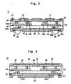
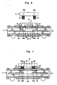
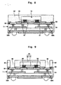
- Figs. 2 to 11 are views showing a manufacturing process of the electronic component embedded board according to the first embodiment of this invention.
- like reference symbols refer to like constituent portions in the electronic component embedded board 10 shown in Fig. 1.
- the first substrate 11 is formed which includes the first multilayered wiring structure 18, protective films 24, 25, and external connecting terminals 26 (first step in claim). Thereafter, an electric test is made for the first substrate 11 with the first multilayered wiring structure 18, thereby providing the first substrate 11 which is a non-defective product.
- the second substrate 12 is formed which includes the second multilayered wiring structure 41 and protective films 42, 43 (second step in claim). Thereafter, an electric test is made for the second substrate 12 with the second multilayered wiring structure 41, thereby providing the second substrate 12 which is a non-defective product.
- a first photosensitive resin 61 having adhesion is formed so as to cover the upper face of the first substrate 11 (the face on the side where the protective film 24 and the connecting areas 33A, 34A are formed).
- the photosensitive resin film having adhesion is affixed to the upper face of the first substrate 11.
- the photosensitive resin film may be made of e.g. epoxy resin or novolac resin doped with a photoreaction initiator.
- the photosensitive resin film can have a thickness of e.g. 30 ⁇ m to 50 ⁇ m.
- the first photosensitive resin 61 is a photosensitive resin having adhesion (capable of keeping adhesion) even after it has been subjected to exposure and development processing.
- the first photosensitive resin 61 can be easily formed as compared with the case where a liquid photosensitive resin having adhesion is used.
- the first photosensitive resin 61 is subjected to exposure and development processing to form the openings 55 exposing the connecting areas 34A and remove the first photosensitive resin 61 formed on the area other than an electronic component arranging region A.
- the electronic component arranging area A refers to a region on the first photosensitive resin 61 in contact with the electronic component 13.
- the conductive members 15 are formed on the electrode pads 13A of the electronic component 13.
- pillar-shaped solders are formed on the electrode pads 13A of the electronic component 13.
- the electronic component 13 is bonded to the first photosensitive resin 61 having adhesion.
- the conductive members 15 being inserted in the openings 55, by heating, the conductive members 15 are molten to connect the conductive members 15 to the connecting areas 34A (third step in claim).
- the electronic component 13 is electrically connected to the first multiple-layer structure 18.
- the heating condition in melting the conductive members 15 can be set as the temperature of 230 to 250°C and the heating time of about several seconds to 10 seconds.
- a second photosensitive resin 62 having adhesion is formed so as to cover the upper face of the structure shown in Fig. 7 (fourth step in claim).
- the photosensitive resin film is affixed to the upper face of the structure of the structure shown in Fig. 7.
- the photosensitive resin film may be made of e.g. epoxy resin or novolac resin doped with a photo initiator.
- the thickness of the photosensitive resin film may be 100 ⁇ m in the case where the thickness of the electronic component 13 is 50 ⁇ m.
- the second photosensitive resin 62 is a photosensitive resin having adhesion (capable of keeping adhesion) even after it has been subjected to exposure and development processing. Further, after the photosensitive resin film has been affixed, a plate having a flat plane may be pressed on the upper face of the photosensitive resin film to make the upper face of the photosensitive resin film flat.
- the second photosensitive resin 62 can be easily formed as compared with the case where a liquid photosensitive resin having adhesion is used.
- the second photosensitive resin 62 is subjected to exposure and development processing to form the through holes 56 exposing the connecting areas 33A.
- the first photosensitive resin 61 having the openings 55 and the second photosensitive resin 62 having the through holes 56 are formed.
- the conductive members 16 are formed in the connecting areas 47A of the second substrate 12 (conductive member forming step).
- the solder or a laminated film composed of Cu, Ni, Au and solder successively stacked on the connecting area 47A is formed.
- Cu, Ni and Au constituting the laminated film can be formed by plating, respectively.
- the second substrate 12 is bonded to the second photosensitive resin 62 having adhesion.
- the conductive members 16 are molten to connect the conductive members 16 to the connecting areas 33A (fifth step in claim).
- the second multilayered wiring structure 41 is electrically connected to the first multilayered wiring structure 18, thus completing the electronic component embedded board 10.
- the heating condition in melting the solder of the conductive members 16 can be set as for example, the temperature of 230 to 250°C and the heating time of about several seconds to 10 seconds.
- the yield of the electronic component embedded board 10 can be improved.
- the space between the first substrate 11 and the second substrate 12 can be accurately sealed as compared with the case where an underfill resin is formed between the first substrate and the second substrate by capillary phenomenon.
- the yield of the electronic component embedded board 10 can be improved.
- the photosensitive resin film as the photosensitive resin 14 having adhesion, the photosensitive resin 14 can be easily formed in a short time.
- the concrete example of the photosensitive resin 14 was explained as an example using the photosensitive resin film.
- the liquid photosensitive resin having adhesion may be applied.
- the liquid photosensitive resin can be formed by e.g. spin coating.
- the photosensitive resin having adhesion was explained as an example of the resin sealing the electric component and bonding the first substrate and the second substrate to each other.
- a nonconductive resin or an anisotropic conductive resin may be applied.
- the nonconductive resin or the anisotropic conductive resin may be e.g. NCF(nonconductive film), NCP(nonconductive paste), ACF(anisotropic conductive film) or ACP(anisotropic conductive paste).
- the processes in Figs. 5 and 9, i.e., the processes of making the openings 55 and through holes 56 in the first and second resins may be omitted. More specifically, the electric component 13 with the conductive member 15 is pressed against the first resin applied on the first substrate 11 so that the conductive member 15 passes through the first resin and then connects to the connecting areas 34A, and then the first resin is cured. Similarly, the second substrate 12 with the conductive member 16 is pressed against the second resin applied on the structure as shown in Fig. 7 so that the conductive member 16 passes through the second resin and then connects to the connecting areas 33A, and then the second resin is cured.
- an underfill resin may be applied between the first substrate 11 and the second substrate 12 by capillary phenomenon.
- the underfill resin may be made of e.g. epoxy resin.
- the underfill resin is applied between the first substrate 11 and the second substrate 12 in a state that the electronic component 13 with the conductive member 15 and the second substrate 12 with the conductive member 16 are provided on the first substrate 11, and then the underfill resin is cured.
- NCF NCF
- NCP NCP
- ACF ACP
- ACP underfill resin
- first and the second substrates 11, 12 were explained as an example using the coreless substrates.
- wiring boards having core substrates may be employed as the first and the second substrates 11, 12. In this case also, the same effect as in this embodiment can be obtained.
- Fig. 12 is a sectional view of the electronic component embedded board according to the second embodiment of this invention.
- like reference symbols refer to like constituent portions in the electronic component embedded board 10 according to the first embodiment.
- the reference symbols for constituent elements in the electronic component embedded board 10 are given "-1"
- the reference symbols for the constituent elements of the structure provided on the electronic component embedded board 10 are given "-2".
- an electronic component embedded board 70 further includes, on the electronic component embedded board 10 explained in the first embodiment, a second substrate 12-2, an electronic component 13-2, a photosensitive resin 14-2 having adhesion, and conductive members 15-2, 16-2.
- the second substrate 12-2 is arranged above the second substrate 12-1 and has a second multilayered wiring structure 41-2.
- the second multilayered wiring structure 41-2 is electrically connected to the second multilayered wiring structure 41-1 of the second substrate 12-1 through the pillar-shaped conductive members 16-2.
- the electronic component 13-2 is arranged between the second substrate 12-1 and the second substrate 12-2.
- the electronic component 13-2 has electrode pads 13A-2.
- the electrode pads 13A-2 are electrically connected to wirings 53-1 through the conductive members 15-2, respectively.
- the electronic component 13-2 is electrically connected to the second multilayered wiring structure 41-1.
- the photosensitive resin 14-2 is arranged between the second substrate 12-1 and the second substrate 12-2.
- the photosensitive resin 14-2 seals the electronic component 13-2 and also bonds the second substrate 12-1 and the second substrate 12-2 to each other.
- the photosensitive resin 14-2 has openings 55-2 and through holes 56-2.
- the openings 55-2 and the through holes 56-2 are made in the photosensitive resin 14-2 formed on the wirings 53-1.
- the openings 55-2 each expose the wiring 53-1 and the through holes 56-2 each expose the wring 53-1 and a connecting area 47A-2.
- the conductive member 15-2 is formed in the opening 55-2, and electrically communicates the electrode pad 13A-2 with the wiring 53-1.
- the conductive member 16-2 is formed in the through hole 56-2 and electrically communicates the wiring 53-1 with the connecting area 47A-2.
- the electronic component embedded board 70 in which three substrates 11, 12-1, 12-2 are stacked so that the electronic components 13-1, 13-2 are arranged between the substrates adjacent to each other in a vertical direction (in this embodiment, between the first substrate 11 and the second substrate 12-1 and between the second substrate 12-1 and the second substrate 12-2) and the substrates adjacent to each other in the vertical direction are bonded by the photosensitive resins 14-1, 14-2 having adhesion, the same effect as in the electronic component embedded board 10 according to the first embodiment can be obtained.
- the case where the three substrates 11, 12-1, 12-2 are stacked was adopted.
- the electronic component embedded board in which three or more substrates are stacked so that the electronic components 13 are arranged between the substrates adjacent in the vertical direction and the substrates adjacent in the vertical direction are bonded by the photosensitive resins 14 having adhesion the same effect as in the electronic component embedded board 10 can be obtained.
- the photosensitive resin having adhesion was explained as an example of the resin sealing the electric component and bonding the first substrate and the second substrate to each other.
- NCF, NCP, ACF, ACP or underfill resin can be used.
- the electronic component embedded board 70 can be manufactured in the same method as the method for manufacturing the electronic component embedded board 10 according to the first embodiment as described previously.
- This invention is applicable to the electronic component embedded board and its manufacturing method capable of the yield.
Landscapes
- Engineering & Computer Science (AREA)
- Manufacturing & Machinery (AREA)
- Microelectronics & Electronic Packaging (AREA)
- Production Of Multi-Layered Print Wiring Board (AREA)
- Non-Metallic Protective Coatings For Printed Circuits (AREA)
Applications Claiming Priority (1)
| Application Number | Priority Date | Filing Date | Title |
|---|---|---|---|
| JP2005264746 | 2005-09-13 |
Publications (2)
| Publication Number | Publication Date |
|---|---|
| EP1763295A2 true EP1763295A2 (fr) | 2007-03-14 |
| EP1763295A3 EP1763295A3 (fr) | 2008-04-30 |
Family
ID=37607202
Family Applications (1)
| Application Number | Title | Priority Date | Filing Date |
|---|---|---|---|
| EP06019174A Withdrawn EP1763295A3 (fr) | 2005-09-13 | 2006-09-13 | Panneau avec des composants enterrés et méthode de fabrication associée |
Country Status (3)
| Country | Link |
|---|---|
| US (1) | US7640655B2 (fr) |
| EP (1) | EP1763295A3 (fr) |
| TW (1) | TW200721934A (fr) |
Cited By (4)
| Publication number | Priority date | Publication date | Assignee | Title |
|---|---|---|---|---|
| EP2228824A1 (fr) * | 2009-03-06 | 2010-09-15 | General Electric Company | Boîtier pour une puce encastrée avec des puces empilées dans un substrat d'interconnexion stratifié |
| EP2478751A4 (fr) * | 2009-09-15 | 2013-01-23 | R & D Circuits Inc | Composants insérés dans une carte intercalaire permettant d'améliorer le gain de puissance (distribution) et la perte de puissance (dissipation) dans une configuration d'interconnexion |
| CN103579081A (zh) * | 2012-07-18 | 2014-02-12 | 万国半导体(开曼)股份有限公司 | 带有芯片尺寸衬底的扇出型半导体器件及制备方法 |
| US8658473B2 (en) | 2012-03-27 | 2014-02-25 | General Electric Company | Ultrathin buried die module and method of manufacturing thereof |
Families Citing this family (28)
| Publication number | Priority date | Publication date | Assignee | Title |
|---|---|---|---|---|
| KR100704919B1 (ko) * | 2005-10-14 | 2007-04-09 | 삼성전기주식회사 | 코어층이 없는 기판 및 그 제조 방법 |
| JP4404139B2 (ja) * | 2005-10-26 | 2010-01-27 | 株式会社村田製作所 | 積層型基板、電子装置および積層型基板の製造方法 |
| TW200843066A (en) * | 2007-04-30 | 2008-11-01 | Chipmos Technologies Inc | Chip stacked package structure and applications thereof |
| JP5215605B2 (ja) * | 2007-07-17 | 2013-06-19 | ラピスセミコンダクタ株式会社 | 半導体装置の製造方法 |
| JP4912992B2 (ja) * | 2007-09-12 | 2012-04-11 | 新光電気工業株式会社 | キャパシタ内蔵基板及びその製造方法 |
| US8225503B2 (en) * | 2008-02-11 | 2012-07-24 | Ibiden Co., Ltd. | Method for manufacturing board with built-in electronic elements |
| US8334590B1 (en) * | 2008-09-04 | 2012-12-18 | Amkor Technology, Inc. | Semiconductor device having insulating and interconnection layers |
| JPWO2010052942A1 (ja) * | 2008-11-06 | 2012-04-05 | イビデン株式会社 | 電子部品内蔵配線板及びその製造方法 |
| JP2010205851A (ja) * | 2009-03-02 | 2010-09-16 | Shinko Electric Ind Co Ltd | 半導体装置及びその製造方法、並びに電子装置 |
| US8743554B2 (en) * | 2009-05-04 | 2014-06-03 | R & D Circuits, Inc. | Apparatus for improved power distribution or power dissipation to an electrical component and method for the same |
| TWI399140B (zh) | 2009-06-12 | 2013-06-11 | 欣興電子股份有限公司 | 內埋式封裝結構的製作方法 |
| TWI393233B (zh) * | 2009-08-18 | 2013-04-11 | 欣興電子股份有限公司 | 無核心層封裝基板及其製法 |
| US8432022B1 (en) | 2009-09-29 | 2013-04-30 | Amkor Technology, Inc. | Shielded embedded electronic component substrate fabrication method and structure |
| US8796561B1 (en) * | 2009-10-05 | 2014-08-05 | Amkor Technology, Inc. | Fan out build up substrate stackable package and method |
| KR101095130B1 (ko) * | 2009-12-01 | 2011-12-16 | 삼성전기주식회사 | 전자부품 내장형 인쇄회로기판 및 그 제조방법 |
| TWI416700B (zh) * | 2009-12-29 | 2013-11-21 | 南茂科技股份有限公司 | 晶片堆疊封裝結構及其製造方法 |
| US10192796B2 (en) * | 2012-09-14 | 2019-01-29 | STATS ChipPAC Pte. Ltd. | Semiconductor device and method of forming dual-sided interconnect structures in FO-WLCSP |
| US8866287B2 (en) | 2012-09-29 | 2014-10-21 | Intel Corporation | Embedded structures for package-on-package architecture |
| CN105393351A (zh) * | 2013-08-21 | 2016-03-09 | 英特尔公司 | 用于无凸起内建层(bbul)的无凸起管芯封装接口 |
| US9576917B1 (en) * | 2013-11-18 | 2017-02-21 | Amkor Technology, Inc. | Embedded die in panel method and structure |
| US9392695B2 (en) * | 2014-01-03 | 2016-07-12 | Samsung Electro-Mechanics Co., Ltd. | Electric component module |
| JP6444269B2 (ja) * | 2015-06-19 | 2018-12-26 | 新光電気工業株式会社 | 電子部品装置及びその製造方法 |
| CN106356355B (zh) * | 2015-07-15 | 2020-06-26 | 恒劲科技股份有限公司 | 基板结构及其制作方法 |
| KR101933408B1 (ko) * | 2015-11-10 | 2018-12-28 | 삼성전기 주식회사 | 전자부품 패키지 및 이를 포함하는 전자기기 |
| US11201136B2 (en) * | 2020-03-10 | 2021-12-14 | International Business Machines Corporation | High bandwidth module |
| CN111863775B (zh) * | 2020-06-16 | 2022-07-26 | 珠海越亚半导体股份有限公司 | 散热兼电磁屏蔽嵌埋封装结构及其制作方法和基板 |
| CN113851383A (zh) * | 2021-08-12 | 2021-12-28 | 日月光半导体制造股份有限公司 | 扇出式基板及其形成方法 |
| CN114666995B (zh) * | 2022-02-25 | 2024-03-26 | 珠海越亚半导体股份有限公司 | 封装基板及其制作方法 |
Family Cites Families (8)
| Publication number | Priority date | Publication date | Assignee | Title |
|---|---|---|---|---|
| US5306670A (en) * | 1993-02-09 | 1994-04-26 | Texas Instruments Incorporated | Multi-chip integrated circuit module and method for fabrication thereof |
| JPH10294423A (ja) * | 1997-04-17 | 1998-11-04 | Nec Corp | 半導体装置 |
| JPH11274734A (ja) | 1998-03-20 | 1999-10-08 | Sony Corp | 電子回路装置およびその製造方法 |
| JP2001007472A (ja) | 1999-06-17 | 2001-01-12 | Sony Corp | 電子回路装置およびその製造方法 |
| US6538210B2 (en) * | 1999-12-20 | 2003-03-25 | Matsushita Electric Industrial Co., Ltd. | Circuit component built-in module, radio device having the same, and method for producing the same |
| US7394663B2 (en) * | 2003-02-18 | 2008-07-01 | Matsushita Electric Industrial Co., Ltd. | Electronic component built-in module and method of manufacturing the same |
| JP2004266074A (ja) * | 2003-02-28 | 2004-09-24 | Olympus Corp | 配線基板 |
| US20060042832A1 (en) * | 2004-08-27 | 2006-03-02 | Kiyoshi Sato | Multilayer circuit board and method of producing the same |
-
2006
- 2006-09-12 US US11/519,125 patent/US7640655B2/en active Active
- 2006-09-13 TW TW095133778A patent/TW200721934A/zh unknown
- 2006-09-13 EP EP06019174A patent/EP1763295A3/fr not_active Withdrawn
Cited By (8)
| Publication number | Priority date | Publication date | Assignee | Title |
|---|---|---|---|---|
| EP2228824A1 (fr) * | 2009-03-06 | 2010-09-15 | General Electric Company | Boîtier pour une puce encastrée avec des puces empilées dans un substrat d'interconnexion stratifié |
| CN101877348A (zh) * | 2009-03-06 | 2010-11-03 | 通用电气公司 | 用于堆叠的管芯嵌入式芯片堆积的系统和方法 |
| US8008125B2 (en) | 2009-03-06 | 2011-08-30 | General Electric Company | System and method for stacked die embedded chip build-up |
| EP2478751A4 (fr) * | 2009-09-15 | 2013-01-23 | R & D Circuits Inc | Composants insérés dans une carte intercalaire permettant d'améliorer le gain de puissance (distribution) et la perte de puissance (dissipation) dans une configuration d'interconnexion |
| US8658473B2 (en) | 2012-03-27 | 2014-02-25 | General Electric Company | Ultrathin buried die module and method of manufacturing thereof |
| US9236348B2 (en) | 2012-03-27 | 2016-01-12 | General Electric Company | Ultrathin buried die module and method of manufacturing thereof |
| CN103579081A (zh) * | 2012-07-18 | 2014-02-12 | 万国半导体(开曼)股份有限公司 | 带有芯片尺寸衬底的扇出型半导体器件及制备方法 |
| CN103579081B (zh) * | 2012-07-18 | 2016-03-02 | 万国半导体(开曼)股份有限公司 | 带有芯片尺寸衬底的扇出型半导体器件及制备方法 |
Also Published As
| Publication number | Publication date |
|---|---|
| TW200721934A (en) | 2007-06-01 |
| US7640655B2 (en) | 2010-01-05 |
| US20070056766A1 (en) | 2007-03-15 |
| EP1763295A3 (fr) | 2008-04-30 |
Similar Documents
| Publication | Publication Date | Title |
|---|---|---|
| EP1763295A2 (fr) | Panneau avec des composants enterrés et méthode de fabrication associée | |
| US8198140B2 (en) | Wiring substrate for mounting semiconductors, method of manufacturing the same, and semiconductor package | |
| KR100232414B1 (ko) | 다층회로기판 및 그 제조방법 | |
| KR100987688B1 (ko) | 프린트 배선 기판 및 프린트 배선 기판의 제조 방법 | |
| KR101027711B1 (ko) | 다층 배선 기판의 제조 방법 | |
| US20090310323A1 (en) | Printed circuit board including electronic component embedded therein and method of manufacturing the same | |
| US9935053B2 (en) | Electronic component integrated substrate | |
| WO2008111546A2 (fr) | Dispositif à semi-conducteur comprenant des éléments structuraux de semi-conducteur sur ses surfaces supérieure et inférieure, et procédé de production de ce dispositif | |
| US20100059876A1 (en) | Electronic component package and method of manufacturing the same | |
| KR20070059186A (ko) | 상호접속 소자를 제조하는 구조와 방법, 및 이 상호접속소자를 포함하는 다층 배선 기판 | |
| TW201405745A (zh) | 晶片封裝基板、晶片封裝結構及其製作方法 | |
| JP4950743B2 (ja) | 積層配線基板及びその製造方法 | |
| JP5238182B2 (ja) | 積層配線基板の製造方法 | |
| KR20080073648A (ko) | 다층 배선 기판 및 그 제조 방법 | |
| CN107770946B (zh) | 印刷布线板及其制造方法 | |
| JP2009146940A (ja) | 積層配線基板及びその製造方法 | |
| JPH10335528A (ja) | 半導体パッケージおよび半導体パッケージの製造方法 | |
| JP4870501B2 (ja) | 電子部品内蔵基板の製造方法 | |
| KR20070030700A (ko) | 전자 부품 내장 기판 및 그 제조 방법 | |
| JP3918828B2 (ja) | 半導体装置 | |
| US9673063B2 (en) | Terminations | |
| CN108305864B (zh) | 端子 | |
| KR101543031B1 (ko) | 인쇄회로기판 및 그 제조 방법 | |
| JP4593444B2 (ja) | 電子部品実装構造体の製造方法 | |
| JPH11260961A (ja) | 半導体搭載用基板とその製造方法及び半導体チップの実装方法 |
Legal Events
| Date | Code | Title | Description |
|---|---|---|---|
| PUAI | Public reference made under article 153(3) epc to a published international application that has entered the european phase |
Free format text: ORIGINAL CODE: 0009012 |
|
| AK | Designated contracting states |
Kind code of ref document: A2 Designated state(s): AT BE BG CH CY CZ DE DK EE ES FI FR GB GR HU IE IS IT LI LT LU LV MC NL PL PT RO SE SI SK TR |
|
| AX | Request for extension of the european patent |
Extension state: AL BA HR MK YU |
|
| PUAL | Search report despatched |
Free format text: ORIGINAL CODE: 0009013 |
|
| AK | Designated contracting states |
Kind code of ref document: A3 Designated state(s): AT BE BG CH CY CZ DE DK EE ES FI FR GB GR HU IE IS IT LI LT LU LV MC NL PL PT RO SE SI SK TR |
|
| AX | Request for extension of the european patent |
Extension state: AL BA HR MK RS |
|
| 17P | Request for examination filed |
Effective date: 20080822 |
|
| AKX | Designation fees paid |
Designated state(s): DE |
|
| GRAP | Despatch of communication of intention to grant a patent |
Free format text: ORIGINAL CODE: EPIDOSNIGR1 |
|
| STAA | Information on the status of an ep patent application or granted ep patent |
Free format text: STATUS: THE APPLICATION IS DEEMED TO BE WITHDRAWN |
|
| 18D | Application deemed to be withdrawn |
Effective date: 20130403 |