EP1764886B1 - Microlaser à déclenchement passif avec densité de puissance de crête controlée - Google Patents
Microlaser à déclenchement passif avec densité de puissance de crête controlée Download PDFInfo
- Publication number
- EP1764886B1 EP1764886B1 EP06120955.7A EP06120955A EP1764886B1 EP 1764886 B1 EP1764886 B1 EP 1764886B1 EP 06120955 A EP06120955 A EP 06120955A EP 1764886 B1 EP1764886 B1 EP 1764886B1
- Authority
- EP
- European Patent Office
- Prior art keywords
- microlaser
- medium
- laser
- laser beam
- gain medium
- Prior art date
- Legal status (The legal status is an assumption and is not a legal conclusion. Google has not performed a legal analysis and makes no representation as to the accuracy of the status listed.)
- Active
Links
- 230000003287 optical effect Effects 0.000 claims description 71
- 239000006096 absorbing agent Substances 0.000 claims description 57
- 238000006073 displacement reaction Methods 0.000 claims description 11
- 230000000694 effects Effects 0.000 claims description 8
- 230000008859 change Effects 0.000 claims description 6
- 239000000463 material Substances 0.000 description 15
- 238000013461 design Methods 0.000 description 14
- 238000013519 translation Methods 0.000 description 13
- 230000008901 benefit Effects 0.000 description 8
- 230000007423 decrease Effects 0.000 description 7
- 230000005284 excitation Effects 0.000 description 6
- 238000010521 absorption reaction Methods 0.000 description 5
- 238000005086 pumping Methods 0.000 description 5
- 238000000576 coating method Methods 0.000 description 4
- 230000001154 acute effect Effects 0.000 description 3
- 238000004458 analytical method Methods 0.000 description 3
- 238000004061 bleaching Methods 0.000 description 3
- 238000010168 coupling process Methods 0.000 description 3
- 238000005859 coupling reaction Methods 0.000 description 3
- 239000013078 crystal Substances 0.000 description 3
- 230000003247 decreasing effect Effects 0.000 description 3
- 238000003754 machining Methods 0.000 description 3
- 238000000816 matrix-assisted laser desorption--ionisation Methods 0.000 description 3
- 238000002310 reflectometry Methods 0.000 description 3
- 239000004065 semiconductor Substances 0.000 description 3
- 230000035945 sensitivity Effects 0.000 description 3
- 238000002834 transmittance Methods 0.000 description 3
- 238000004364 calculation method Methods 0.000 description 2
- 230000008878 coupling Effects 0.000 description 2
- 238000004519 manufacturing process Methods 0.000 description 2
- 230000007246 mechanism Effects 0.000 description 2
- 239000012071 phase Substances 0.000 description 2
- 239000007787 solid Substances 0.000 description 2
- 238000013459 approach Methods 0.000 description 1
- 201000009310 astigmatism Diseases 0.000 description 1
- 230000005540 biological transmission Effects 0.000 description 1
- 230000015572 biosynthetic process Effects 0.000 description 1
- 239000011248 coating agent Substances 0.000 description 1
- 238000005094 computer simulation Methods 0.000 description 1
- 238000010276 construction Methods 0.000 description 1
- 238000009792 diffusion process Methods 0.000 description 1
- 230000002349 favourable effect Effects 0.000 description 1
- 230000003116 impacting effect Effects 0.000 description 1
- 230000003993 interaction Effects 0.000 description 1
- 238000004943 liquid phase epitaxy Methods 0.000 description 1
- 238000000034 method Methods 0.000 description 1
- 230000001151 other effect Effects 0.000 description 1
- 238000012545 processing Methods 0.000 description 1
- 238000010561 standard procedure Methods 0.000 description 1
- 239000000758 substrate Substances 0.000 description 1
Images


Classifications
-
- H—ELECTRICITY
- H01—ELECTRIC ELEMENTS
- H01S—DEVICES USING THE PROCESS OF LIGHT AMPLIFICATION BY STIMULATED EMISSION OF RADIATION [LASER] TO AMPLIFY OR GENERATE LIGHT; DEVICES USING STIMULATED EMISSION OF ELECTROMAGNETIC RADIATION IN WAVE RANGES OTHER THAN OPTICAL
- H01S3/00—Lasers, i.e. devices using stimulated emission of electromagnetic radiation in the infrared, visible or ultraviolet wave range
- H01S3/05—Construction or shape of optical resonators; Accommodation of active medium therein; Shape of active medium
- H01S3/06—Construction or shape of active medium
- H01S3/0627—Construction or shape of active medium the resonator being monolithic, e.g. microlaser
-
- H—ELECTRICITY
- H01—ELECTRIC ELEMENTS
- H01S—DEVICES USING THE PROCESS OF LIGHT AMPLIFICATION BY STIMULATED EMISSION OF RADIATION [LASER] TO AMPLIFY OR GENERATE LIGHT; DEVICES USING STIMULATED EMISSION OF ELECTROMAGNETIC RADIATION IN WAVE RANGES OTHER THAN OPTICAL
- H01S3/00—Lasers, i.e. devices using stimulated emission of electromagnetic radiation in the infrared, visible or ultraviolet wave range
- H01S3/02—Constructional details
- H01S3/025—Constructional details of solid state lasers, e.g. housings or mountings
-
- H—ELECTRICITY
- H01—ELECTRIC ELEMENTS
- H01S—DEVICES USING THE PROCESS OF LIGHT AMPLIFICATION BY STIMULATED EMISSION OF RADIATION [LASER] TO AMPLIFY OR GENERATE LIGHT; DEVICES USING STIMULATED EMISSION OF ELECTROMAGNETIC RADIATION IN WAVE RANGES OTHER THAN OPTICAL
- H01S3/00—Lasers, i.e. devices using stimulated emission of electromagnetic radiation in the infrared, visible or ultraviolet wave range
- H01S3/05—Construction or shape of optical resonators; Accommodation of active medium therein; Shape of active medium
- H01S3/06—Construction or shape of active medium
- H01S3/063—Waveguide lasers, i.e. whereby the dimensions of the waveguide are of the order of the light wavelength
- H01S3/067—Fibre lasers
- H01S3/06754—Fibre amplifiers
-
- H—ELECTRICITY
- H01—ELECTRIC ELEMENTS
- H01S—DEVICES USING THE PROCESS OF LIGHT AMPLIFICATION BY STIMULATED EMISSION OF RADIATION [LASER] TO AMPLIFY OR GENERATE LIGHT; DEVICES USING STIMULATED EMISSION OF ELECTROMAGNETIC RADIATION IN WAVE RANGES OTHER THAN OPTICAL
- H01S3/00—Lasers, i.e. devices using stimulated emission of electromagnetic radiation in the infrared, visible or ultraviolet wave range
- H01S3/09—Processes or apparatus for excitation, e.g. pumping
- H01S3/091—Processes or apparatus for excitation, e.g. pumping using optical pumping
- H01S3/094—Processes or apparatus for excitation, e.g. pumping using optical pumping by coherent light
- H01S3/0941—Processes or apparatus for excitation, e.g. pumping using optical pumping by coherent light of a laser diode
- H01S3/09415—Processes or apparatus for excitation, e.g. pumping using optical pumping by coherent light of a laser diode the pumping beam being parallel to the lasing mode of the pumped medium, e.g. end-pumping
-
- H—ELECTRICITY
- H01—ELECTRIC ELEMENTS
- H01S—DEVICES USING THE PROCESS OF LIGHT AMPLIFICATION BY STIMULATED EMISSION OF RADIATION [LASER] TO AMPLIFY OR GENERATE LIGHT; DEVICES USING STIMULATED EMISSION OF ELECTROMAGNETIC RADIATION IN WAVE RANGES OTHER THAN OPTICAL
- H01S3/00—Lasers, i.e. devices using stimulated emission of electromagnetic radiation in the infrared, visible or ultraviolet wave range
- H01S3/10—Controlling the intensity, frequency, phase, polarisation or direction of the emitted radiation, e.g. switching, gating, modulating or demodulating
- H01S3/102—Controlling the intensity, frequency, phase, polarisation or direction of the emitted radiation, e.g. switching, gating, modulating or demodulating by controlling the active medium, e.g. by controlling the processes or apparatus for excitation
- H01S3/1022—Controlling the intensity, frequency, phase, polarisation or direction of the emitted radiation, e.g. switching, gating, modulating or demodulating by controlling the active medium, e.g. by controlling the processes or apparatus for excitation by controlling the optical pumping
-
- H—ELECTRICITY
- H01—ELECTRIC ELEMENTS
- H01S—DEVICES USING THE PROCESS OF LIGHT AMPLIFICATION BY STIMULATED EMISSION OF RADIATION [LASER] TO AMPLIFY OR GENERATE LIGHT; DEVICES USING STIMULATED EMISSION OF ELECTROMAGNETIC RADIATION IN WAVE RANGES OTHER THAN OPTICAL
- H01S3/00—Lasers, i.e. devices using stimulated emission of electromagnetic radiation in the infrared, visible or ultraviolet wave range
- H01S3/10—Controlling the intensity, frequency, phase, polarisation or direction of the emitted radiation, e.g. switching, gating, modulating or demodulating
- H01S3/11—Mode locking; Q-switching; Other giant-pulse techniques, e.g. cavity dumping
- H01S3/1123—Q-switching
- H01S3/113—Q-switching using intracavity saturable absorbers
-
- H—ELECTRICITY
- H01—ELECTRIC ELEMENTS
- H01S—DEVICES USING THE PROCESS OF LIGHT AMPLIFICATION BY STIMULATED EMISSION OF RADIATION [LASER] TO AMPLIFY OR GENERATE LIGHT; DEVICES USING STIMULATED EMISSION OF ELECTROMAGNETIC RADIATION IN WAVE RANGES OTHER THAN OPTICAL
- H01S3/00—Lasers, i.e. devices using stimulated emission of electromagnetic radiation in the infrared, visible or ultraviolet wave range
- H01S3/23—Arrangements of two or more lasers not provided for in groups H01S3/02 - H01S3/22, e.g. tandem arrangements of separate active media
- H01S3/2375—Hybrid lasers
-
- H—ELECTRICITY
- H01—ELECTRIC ELEMENTS
- H01S—DEVICES USING THE PROCESS OF LIGHT AMPLIFICATION BY STIMULATED EMISSION OF RADIATION [LASER] TO AMPLIFY OR GENERATE LIGHT; DEVICES USING STIMULATED EMISSION OF ELECTROMAGNETIC RADIATION IN WAVE RANGES OTHER THAN OPTICAL
- H01S3/00—Lasers, i.e. devices using stimulated emission of electromagnetic radiation in the infrared, visible or ultraviolet wave range
- H01S3/005—Optical devices external to the laser cavity, specially adapted for lasers, e.g. for homogenisation of the beam or for manipulating laser pulses, e.g. pulse shaping
-
- H—ELECTRICITY
- H01—ELECTRIC ELEMENTS
- H01S—DEVICES USING THE PROCESS OF LIGHT AMPLIFICATION BY STIMULATED EMISSION OF RADIATION [LASER] TO AMPLIFY OR GENERATE LIGHT; DEVICES USING STIMULATED EMISSION OF ELECTROMAGNETIC RADIATION IN WAVE RANGES OTHER THAN OPTICAL
- H01S3/00—Lasers, i.e. devices using stimulated emission of electromagnetic radiation in the infrared, visible or ultraviolet wave range
- H01S3/02—Constructional details
- H01S3/04—Arrangements for thermal management
- H01S3/0405—Conductive cooling, e.g. by heat sinks or thermo-electric elements
-
- H—ELECTRICITY
- H01—ELECTRIC ELEMENTS
- H01S—DEVICES USING THE PROCESS OF LIGHT AMPLIFICATION BY STIMULATED EMISSION OF RADIATION [LASER] TO AMPLIFY OR GENERATE LIGHT; DEVICES USING STIMULATED EMISSION OF ELECTROMAGNETIC RADIATION IN WAVE RANGES OTHER THAN OPTICAL
- H01S3/00—Lasers, i.e. devices using stimulated emission of electromagnetic radiation in the infrared, visible or ultraviolet wave range
- H01S3/02—Constructional details
- H01S3/04—Arrangements for thermal management
- H01S3/042—Arrangements for thermal management for solid state lasers
-
- H—ELECTRICITY
- H01—ELECTRIC ELEMENTS
- H01S—DEVICES USING THE PROCESS OF LIGHT AMPLIFICATION BY STIMULATED EMISSION OF RADIATION [LASER] TO AMPLIFY OR GENERATE LIGHT; DEVICES USING STIMULATED EMISSION OF ELECTROMAGNETIC RADIATION IN WAVE RANGES OTHER THAN OPTICAL
- H01S3/00—Lasers, i.e. devices using stimulated emission of electromagnetic radiation in the infrared, visible or ultraviolet wave range
- H01S3/05—Construction or shape of optical resonators; Accommodation of active medium therein; Shape of active medium
- H01S3/06—Construction or shape of active medium
- H01S3/0602—Crystal lasers or glass lasers
- H01S3/0606—Crystal lasers or glass lasers with polygonal cross-section, e.g. slab, prism
-
- H—ELECTRICITY
- H01—ELECTRIC ELEMENTS
- H01S—DEVICES USING THE PROCESS OF LIGHT AMPLIFICATION BY STIMULATED EMISSION OF RADIATION [LASER] TO AMPLIFY OR GENERATE LIGHT; DEVICES USING STIMULATED EMISSION OF ELECTROMAGNETIC RADIATION IN WAVE RANGES OTHER THAN OPTICAL
- H01S3/00—Lasers, i.e. devices using stimulated emission of electromagnetic radiation in the infrared, visible or ultraviolet wave range
- H01S3/05—Construction or shape of optical resonators; Accommodation of active medium therein; Shape of active medium
- H01S3/06—Construction or shape of active medium
- H01S3/0602—Crystal lasers or glass lasers
- H01S3/0612—Non-homogeneous structure
-
- H—ELECTRICITY
- H01—ELECTRIC ELEMENTS
- H01S—DEVICES USING THE PROCESS OF LIGHT AMPLIFICATION BY STIMULATED EMISSION OF RADIATION [LASER] TO AMPLIFY OR GENERATE LIGHT; DEVICES USING STIMULATED EMISSION OF ELECTROMAGNETIC RADIATION IN WAVE RANGES OTHER THAN OPTICAL
- H01S3/00—Lasers, i.e. devices using stimulated emission of electromagnetic radiation in the infrared, visible or ultraviolet wave range
- H01S3/09—Processes or apparatus for excitation, e.g. pumping
- H01S3/091—Processes or apparatus for excitation, e.g. pumping using optical pumping
- H01S3/094—Processes or apparatus for excitation, e.g. pumping using optical pumping by coherent light
- H01S3/094049—Guiding of the pump light
- H01S3/094053—Fibre coupled pump, e.g. delivering pump light using a fibre or a fibre bundle
-
- H—ELECTRICITY
- H01—ELECTRIC ELEMENTS
- H01S—DEVICES USING THE PROCESS OF LIGHT AMPLIFICATION BY STIMULATED EMISSION OF RADIATION [LASER] TO AMPLIFY OR GENERATE LIGHT; DEVICES USING STIMULATED EMISSION OF ELECTROMAGNETIC RADIATION IN WAVE RANGES OTHER THAN OPTICAL
- H01S3/00—Lasers, i.e. devices using stimulated emission of electromagnetic radiation in the infrared, visible or ultraviolet wave range
- H01S3/09—Processes or apparatus for excitation, e.g. pumping
- H01S3/091—Processes or apparatus for excitation, e.g. pumping using optical pumping
- H01S3/094—Processes or apparatus for excitation, e.g. pumping using optical pumping by coherent light
- H01S3/094076—Pulsed or modulated pumping
-
- H—ELECTRICITY
- H01—ELECTRIC ELEMENTS
- H01S—DEVICES USING THE PROCESS OF LIGHT AMPLIFICATION BY STIMULATED EMISSION OF RADIATION [LASER] TO AMPLIFY OR GENERATE LIGHT; DEVICES USING STIMULATED EMISSION OF ELECTROMAGNETIC RADIATION IN WAVE RANGES OTHER THAN OPTICAL
- H01S3/00—Lasers, i.e. devices using stimulated emission of electromagnetic radiation in the infrared, visible or ultraviolet wave range
- H01S3/10—Controlling the intensity, frequency, phase, polarisation or direction of the emitted radiation, e.g. switching, gating, modulating or demodulating
- H01S3/101—Lasers provided with means to change the location from which, or the direction in which, laser radiation is emitted
-
- H—ELECTRICITY
- H01—ELECTRIC ELEMENTS
- H01S—DEVICES USING THE PROCESS OF LIGHT AMPLIFICATION BY STIMULATED EMISSION OF RADIATION [LASER] TO AMPLIFY OR GENERATE LIGHT; DEVICES USING STIMULATED EMISSION OF ELECTROMAGNETIC RADIATION IN WAVE RANGES OTHER THAN OPTICAL
- H01S3/00—Lasers, i.e. devices using stimulated emission of electromagnetic radiation in the infrared, visible or ultraviolet wave range
- H01S3/10—Controlling the intensity, frequency, phase, polarisation or direction of the emitted radiation, e.g. switching, gating, modulating or demodulating
- H01S3/102—Controlling the intensity, frequency, phase, polarisation or direction of the emitted radiation, e.g. switching, gating, modulating or demodulating by controlling the active medium, e.g. by controlling the processes or apparatus for excitation
- H01S3/1026—Controlling the active medium by translation or rotation, e.g. to remove heat from that part of the active medium that is situated on the resonator axis
-
- H—ELECTRICITY
- H01—ELECTRIC ELEMENTS
- H01S—DEVICES USING THE PROCESS OF LIGHT AMPLIFICATION BY STIMULATED EMISSION OF RADIATION [LASER] TO AMPLIFY OR GENERATE LIGHT; DEVICES USING STIMULATED EMISSION OF ELECTROMAGNETIC RADIATION IN WAVE RANGES OTHER THAN OPTICAL
- H01S3/00—Lasers, i.e. devices using stimulated emission of electromagnetic radiation in the infrared, visible or ultraviolet wave range
- H01S3/10—Controlling the intensity, frequency, phase, polarisation or direction of the emitted radiation, e.g. switching, gating, modulating or demodulating
- H01S3/106—Controlling the intensity, frequency, phase, polarisation or direction of the emitted radiation, e.g. switching, gating, modulating or demodulating by controlling devices placed within the cavity
- H01S3/108—Controlling the intensity, frequency, phase, polarisation or direction of the emitted radiation, e.g. switching, gating, modulating or demodulating by controlling devices placed within the cavity using non-linear optical devices, e.g. exhibiting Brillouin or Raman scattering
-
- H—ELECTRICITY
- H01—ELECTRIC ELEMENTS
- H01S—DEVICES USING THE PROCESS OF LIGHT AMPLIFICATION BY STIMULATED EMISSION OF RADIATION [LASER] TO AMPLIFY OR GENERATE LIGHT; DEVICES USING STIMULATED EMISSION OF ELECTROMAGNETIC RADIATION IN WAVE RANGES OTHER THAN OPTICAL
- H01S3/00—Lasers, i.e. devices using stimulated emission of electromagnetic radiation in the infrared, visible or ultraviolet wave range
- H01S3/14—Lasers, i.e. devices using stimulated emission of electromagnetic radiation in the infrared, visible or ultraviolet wave range characterised by the material used as the active medium
- H01S3/16—Solid materials
- H01S3/1601—Solid materials characterised by an active (lasing) ion
- H01S3/1603—Solid materials characterised by an active (lasing) ion rare earth
- H01S3/1611—Solid materials characterised by an active (lasing) ion rare earth neodymium
-
- H—ELECTRICITY
- H01—ELECTRIC ELEMENTS
- H01S—DEVICES USING THE PROCESS OF LIGHT AMPLIFICATION BY STIMULATED EMISSION OF RADIATION [LASER] TO AMPLIFY OR GENERATE LIGHT; DEVICES USING STIMULATED EMISSION OF ELECTROMAGNETIC RADIATION IN WAVE RANGES OTHER THAN OPTICAL
- H01S3/00—Lasers, i.e. devices using stimulated emission of electromagnetic radiation in the infrared, visible or ultraviolet wave range
- H01S3/14—Lasers, i.e. devices using stimulated emission of electromagnetic radiation in the infrared, visible or ultraviolet wave range characterised by the material used as the active medium
- H01S3/16—Solid materials
- H01S3/163—Solid materials characterised by a crystal matrix
- H01S3/164—Solid materials characterised by a crystal matrix garnet
- H01S3/1643—YAG
Definitions
- the present invention relates to pulsed microchip lasers, in particular those having tunable output performance based on variably filled cavity and variable-focus optics:
- Passively Q-switched microchip lasers have many advantages: they allow the realization of low-cost, compact and robust laser sources. Because of the short cavity length, they are capable of generating pulses with high peak power, which are particularly convenient for generation of harmonics (e.g. ultraviolet lasers). High peak power is of primary interest for many applications such as marking, excitation of fluorescence, ionization of solids such as matrix-assisted laser desorption ionization (MALDI) for proteomics, long distance time-of-flight ranging, generation of supercontinuum, and others.
- MALDI matrix-assisted laser desorption ionization
- the output performance parameters (pulse duration, energy, and repetition rate) of passively Q-switched lasers based on saturable absorbers depend primarily on the design of the microchip laser cavity. These include the optical path length through the different materials, magnitude of gain in the active medium, saturable and non-saturable losses, output coupling, length of the cavity. According to basic laser equations, the main trends are :
- the pulse duration is approximately constant, while the pulse energy does not vary with pump power if the focusing of the pump is unchanged.
- repetition rate is the sole performance parameter that can be controlled through pump power only. To achieve control of the peak power, a more complex design of laser is involved.
- Another alternative would be to use an output-coupling mirror with a reflection coefficient that varies across the surface of the microchip, so that the cavity losses could be adjusted by translating the microlaser laterally.
- this solution is also not very practical and technically very difficult to implement given the typical lateral dimensions of a microlaser. It would also be very expensive since it would require that every microchip be coated independently, thereby losing the benefit of mass processing, which is a major advantage that the microchip concept has introduced.
- the laser output parameters of a passively Q-switched microchip laser can be controlled by varying the lengths of gain media and saturable absorber media that are present within the laser cavity.
- Shinichi Japanese Patent JP 07-131102,A , Toshiba discloses a laser cavity configuration in which the optical path length through the gain media remains constant as the optical path length through the saturable absorber is varied by the displacement of a wedge-shaped prism transversely-to the cavity optical axis.
- This patent does not disclose a means for changing the length of the gain media in the optical cavity and all figures in the patent show a cavity gain media of constant length.
- the patent application discloses a solid-state laser resonator that has an interface inclined from a plane orthogonal to the optical axis of the excitation light.
- the light path length of the solid-state resonator in the direction parallel to the optical axis of the excitation light differs depending on setting of the position of excitation. That is, the light path length of the resonator can be specified or can be adjusted depending on the setting of the position of excitation in the direction orthogonal to the optical axis of the excitation light.
- the variation of the optical length of the cavity is very limited (less than one wavelength), which is not enough for yielding a broad range of control of the output performance.
- the cavity is also misaligned, whereby losses are increased and performance reduced.
- the main purpose of this patent is to provide a convenient way of controlling the longitudinal modes in the cavity, and then of finding stable operation rather than to vary the pulse parameters.
- Sumida (US Patent 5,303,256 , Hughes Aircraft Company) emphasizes the use of a non-doped wedge in order to avoid any variation or non-homogeneity of the performance. It does not, however, report (or claim) varying the transmission of the saturable absorber to adjust the laser output performance.
- Fukumoto US Pat. 6,466,593 , Raytheon Company discloses a passive Q-switch having a variable thickness, comprising of a pair of saturable absorber wedges mounted so that they can be translated with respect to each other. A means for varying the thickness of the saturable material that is present in the laser cavity is thereby provided. This mechanism adds complexity, and further increases the likelihood of misalignment when adjusting the output parameters.
- a semiconductor passive Q-switch laser with a variable transmittance Q-switch produces variable output suitable for use in a laser system with defined output characteristics.
- the disclosed laser is based on a coating with variable transmittance across the output aperture, the solution is difficult to implement in manufacturing, as coatings have to be applied individually to each laser chip.
- the use of a wedged shape saturable absorber is not detailed in this patent, no embodiment is described, and the claims are limited to coatings with variable transmittance.
- the patent also teaches the use of a semiconductor wedge that can be translated normal to the laser cavity axis.
- microchip lasers monolithic laser cavities
- the passively Q-switched microchip lasers described by Zayhowski permits the construction of lasers with smaller size, no external control for pulse formation, high peak power, very low sensitivity to misalignment or vibration.
- this patent teaches that output performance is related to the design of the microchip, it gives no method of modifying it in a controllable manner.
- Peterson US Patent 6,668,004
- a passively Q-switched microlaser based on an arrangement of wedged or triangular shaped microchips.
- the purpose of the invention claimed in that patent is to increase the length of the microlaser while preserving the most compact design.
- No reference is made to controlling or varying the output performance of the laser. As the optical path in the microlaser is fixed, no variation of the relative position of the pump beam within the microlaser is considered.
- Neev et al. ( US Pat. Application 2003/039274 ) describes a passively Q-switched microlaser with a monolithic optical cavity comprising a stack of Yb 3+ :YAG gain medium, and Cr 4+ :YAG or LiF 2 saturable absorber between two pieces of undoped YAG medium.
- Optical path lengths within the four cavity components cannot be varied, being fixed for any particular microlaser, as the faces of all four pieces are polished parallel to each other and normal to the optical axis.
- a further disclosure by Masuda et al. ( European Patent Application EP-A2-0 508 406 ) teaches a microlaser for intra-cavity frequency doubling.
- the microlaser has a monolithic optical cavity comprising a quarter wave plate, a laser medium and a non-linear optical crystal element.
- the interface between the laser medium and the non-linear optical crystal element is slightly inclined from a normal incidence to the optical axis for permitting the highest level of second harmonic laser power to be achieved by a lateral adjustment of an optical axis of a pumping laser beam.
- the maximum power corresponds to a phase delay amount of an odd number of quarter wavelengths and an optimal amount of double refraction in the non-linear optical crystal element, which occurs periodically as the optical axis of the pumping laser beam is laterally adjusted.
- the position of the optical axis of the pumping laser is secured in place when the optical path length satisfies the phase delay condition.
- a simplified design is disclosed for varying the optical path lengths of the lasing (gain) and saturable absorber media within the cavity of a passively Q-switched microchip laser.
- the basic configuration according to this disclosure is a laser cavity comprising of a gain medium block and a saturable absorber block that are optically contacted together to form a single parallel-faced block in which the optical contacting plane is tilted with respect to the laser cavity optic axis.
- Translation of the rectangular block normal to the laser cavity axis varies the optical path lengths in the gain media and saturable absorber media that are present in the laser cavity thereby providing a simple means for varying the laser output characteristics.
- the present invention provides for an easy way to control the pulse energy, pulse duration or peak power density of passively Q-switched microlasers by designing the geometry of the laser cavity (e.g. wedged-shaped materials) so that the optical path in the active medium and/or the saturable absorber can be varied by simple displacement of the microlaser.
- Such structures can be produced using standard techniques: diffusion bonding (or optical contacting) of wedged plates, or liquid phase epitaxy of one material on a wedged substrate of the other material.
- combining such a microlaser with variable-focus optics allows the peak power density of the output laser beam to be controlled.
- Such a laser system can be used for direct application, or seed a subsequent amplifier or harmonic generation stages.
- a first exemplary embodiment is described in figure 1 , in which a microchip 30 comprises a wedge-shaped gain medium 1, and a wedge-shaped saturable absorber medium 2, bonded at an interface 20.
- a lasing cavity is defined between an input mirror surface 9 and an output coupler surface 10.
- the surface of the input mirror 9 on the gain medium 1 is coated for high reflectivity at a lasing wavelength, but high transmittivity at a pump wavelength, while that of the output coupler 10 on the saturable absorber medium 2 is coated with a film, which is partially reflecting at the lasing wavelength.
- a pump beam 5 is directed onto the microchip 30, which causes a lasing beam to oscillate along an optical path between the input mirror 9 and the output coupler 10, from which a laser output beam 6 is emitted.
- the interface 20 makes an acute wedge angle with respect to the lasing beam, which traverses an optical path length 11 within the gain medium 1 and an optical path length 12 within the saturable absorber medium 2.
- the magnitude of the acute wedge angle is chosen to provide the desired control sensitivity of the optical path lengths 11 and 12 as the microchip 30 is translated transversely relative to the pump beam 5 along a direction, which is approximately parallel to the input mirror 9 and to the ' x ' axis.
- both gain medium 1, and saturable absorber medium 2 have two faces - an input face and an output face.
- wedged shaped refers to the shape of a cross-section of the medium in a plane perpendicular to both the input and output faces.
- the wedge angle is defined as the angle between the input and output faces at the point where they are intersected by the lasing beam.
- the wedge angle is an acute angle, e.g. non-zero, any lateral translation of the lasing beam with respect to the lasing cavity will produce a corresponding change in the length of the optical path of the lasing beam within the medium bounded by those input and output faces.
- An optical path or an axis is considered 'normal' to a plane if it is perpendicular to that plane, in other words intersects it at 90°.
- the translation is typically effected by a mechanical translation stage 7 aligned parallel to the ' x ' axis, which can be actuated in either direction by a hand-operated worm gear mechanism or by a suitable electrical motor drive or other type of actuator.
- the output performance parameters vary as follows: pulse energy E decreases, pulse period ⁇ increases and pulse repetition rate, f, increases.
- Variation of the absorbed pump power also impacts on microchip temperature. As a consequence, the wavelength of the longitudinal modes shift relatively to the gain curve, and the laser performance changes. A more advanced embodiment of particular interest would then include an additional means for controlling the temperature of the microlaser (e.g. thermoelectric cooler).
- thermoelectric cooler e.g. thermoelectric cooler
- the bonding interface 20 between the saturable absorber 2 and the gain medium 1 can be cylindrical, spherical, or have an arbitrary shape, without departing from the scope of this invention.
- the microchip 30 comprises two or more slabs bonded together perpendicular to the input mirror 9 and extending to the output coupler 10. Each slab has a different length of gain medium 1a and saturable absorber 2a .
- An alternative embodiment can use discrete microchip slabs with similar media but different output couplers reflectivities, with the drawbacks of increased fabrication cost and complexity.
- figure 1 shows the simplest displacement of the laser microchip, i.e. in a plane perpendicular to the saturable absorber/gain medium interface 20 and the input mirror 9.
- the displacement can also be implemented in a different plane without departing from the scope of the present invention, since it will lead to exactly similar effects, as long as it has a projection along the x-axis.
- the pump beam can be moved relatively to the microchip (e.g. by a movable lens or mirror).
- Different embodiments of the invention can be derived from the microchip arrangement of figure 1 by changing the pump mode.
- the above description considers a constant continuous wave pump power.
- a second exemplary embodiment can use a continuous wave pump beam 5, where the pump power is adjusted simultaneously to the translating of the microchip 30. This will, for example, permit the absorbed pump power to be kept constant in order to have a constant pulse repetition rate.
- the pump beam 5 can be operated in a modulated mode, so that the repetition rate of the laser is set by the modulation frequency of the pump.
- the time for build-up of the laser pulse will vary as the microchip 30 is translated.
- the duration of the pump pulses will then advantageously be chosen to be equal to that build-up time, in order to avoid emission of multiple laser pulses in one pump pulse cycle. This can be achieved, for example, by detecting the emission of the laser pulse and applying a feedback to the drive current of the pump.
- This mode of operation is particularly interesting in the context of instant invention, because the variation of the pulse energy and pulse duration can thus be decoupled from the selection of the repetition rate.
- the pump beam 5 can be modulated, and its amplitude varied simultaneously to translating the microlaser in order to control some of the laser performance parameters.
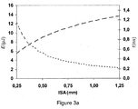
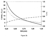
- figure 3 A more detailed analysis of the variation of the output performance with displacement of the microchip 30 is presented on figure 3 , which has been obtained from computer simulations based on the complete set of laser equations, including all effects mentioned above.
- the gain medium is Nd:YAG, with 1.3% Nd 3+ concentration.
- the saturable absorber is Cr 4+ :YAG, with an unsaturated absorption of 6cm -1 .
- the total length of the microchip 30 is 2mm.
- the variation of l SA (x) considered in figure 3a corresponds to a lateral displacement x of 1mm.
- the reflectivity of the output coupler is 85% at 1064nm.
- the pump beam at 808nm is focused with an average radius of 70 ⁇ m. Absorption of the pump was chosen at 7cm -1 .
- the radius of the laser mode in the cavity was fixed at 60 ⁇ m.
- Figure 3a corresponds to a continuous wave pump beam, with a constant power of 1.3W.
- the optical path length l SA , 12 within the saturable absorber is varied from 0.25 mm to 1.25 mm, the pulse energy increases from about 6 ⁇ J to 13 ⁇ J, while the pulse duration is decreased from 1.1 ns to 0.2 ns.
- Figure 3b corresponds to a modulated pump with a repetition rate of 1kHz and a peak power of 1.3W.
- the pulse repetition rate is reduced from 35 kHz to 2 kHz, pulse energy increases from about 6 ⁇ J to 13 ⁇ J, while the pulse duration is decreased from more than 1.1 ns to about 0.2 ns.
- the duration of the pump pulses is equal to the emission delay of one laser pulse (varies with l SA ).
- Operation with modulated pump can be achieved at higher repetition rates with the same microlaser, by either using a higher pump peak power, or by applying a constant offset pump power (as described for example in Fève et al, Advanced Solid State Photonics 2005, paper TuB39).
- Using a modulated pump allows the repetition rate of the laser to be controlled independently.
- the magnitude of the variations of the pulse energy and pulse duration is very similar to the previous case. This solution is particularly interesting from an application point of view.
- FIG. 4a An example of the measured variation of performance that can be achieved is shown in figure 4a .
- the optical path length l SA , 12 within the saturable absorber is varied by about 400% from 0.25 mm to 1.0 mm, pulse energy increases from about 3 ⁇ J to 11 ⁇ J, while the pulse duration is decreased from about 1.0 ns to about 0.4 ns.
- Fig. 4b shows the trend of laser performance as the optical path length l gain , 11, within the gain medium is varied from 0.75 mm to 1.5 mm, an increase of 200%.
- the pulse energy increases from about 2.2 ⁇ J to 3.0 ⁇ J, while the pulse duration is increased from about 0.5 ns to about 1.0 ns.
- the overall microchip forms a plane-parallel cavity to allow resonance whatever the displacement of the microchip with respect to the pump beam. Allowance for a minor departure from parallelism of the output coupler 10 with respect to the input mirror 1 may be required in cases where deviations of the laser beam from a straight line caused refractive index differences between the various media cannot be neglected.
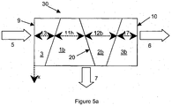
- FIG 5a is an extension of the first exemplary embodiment shown in figure 1 .
- both the wedged gain medium 1b and wedged saturable absorber 2b are sandwiched between two end-caps 3, 3b comprising undoped transparent medium with corresponding optical path lengths 13 and 17 respectively.
- Translation of the microchip 30 in the 'x' direction by the translation stage 7 results in similar effects to those described for the first exemplary embodiment.
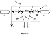
- An equivalent design is shown in figure 5b , where the gain medium is split in two half-wedges 1 and 1c with corresponding optical path lengths 11 and 16 respectively in order to reduce the number of optical parts and bonded interfaces.
- the saturable gain medium 2c is thus fully enclosed within the microchip 30 between interfaces 20 and 20', while the input mirror 9 and the output coupler 10 are formed on the gain medium 1 and 1c respectively.
- Figure 6 shows the geometry of yet another exemplary embodiment that allows similar control of the laser performance.
- the wedge-shaped gain medium 1b is symmetrical about a plane parallel to the input mirror 9 and enclosed between an end-cap 3 comprising undoped transparent medium and saturable absorbing medium 2.
- the optical path lengths 11b and 12 vary in different proportions, in contrast to the first exemplary embodiment, where these proportions are practically equal.
- the slopes ⁇ l SA / ⁇ x and ⁇ l gain / ⁇ x are also larger compared to the geometry of the first exemplary embodiment.
- the physical length of the cavity does not change, while the optical length will depend on the refractive index of the undoped cap compared to the two other materials. If they are equal, l cav is unchanged. This gives an additional degree of freedom for altering the variation of the optical length of the laser, and thus the pulse duration independent of the pulse energy.
- Figure 7 shows a further example embodiment where the interface between the gain medium 1d and the saturable absorbing medium 2 is parallel to the input mirror 9.
- the optical path length 11d within the gain medium 1d stays constant, while only the optical path length 12 within the saturable absorbing medium 2 , l SA , varies under lateral translation of the microchip 30.
- This has the advantage that for a constant pump power the absorbed pump power is independent of the lateral translation, so that thermal effects are constant.
- This geometry permits the optimum focusing of the pump beam to be maintained independently of the position 'x' of the microchip 30. Pre-bleaching of the saturable absorber by unabsorbed pump also stays unchanged.
- the repetition rate will decrease, since losses increase, thus increasing the laser threshold while absorbed pump power stays constant.
- the pump power can also be varied while translating the microchip 30 in order to maintain a constant repetition rate. In both cases, the pulse energy will increase while the pulse duration will be lowered when moving along 'x'.
- This embodiment can also use a modulated pump. There is no need to simultaneously vary the pump power while translating the microlaser, but this may also be done.
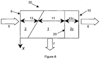
- FIG. 8 Another embodiment is shown in the example of figure 8 where under translation of the microchip 30 along the 'x' direction the optical path length 12c in the saturable absorber 2c does not change while only the optical path length 11 within the gain medium 1, l gain (x), varies. If the pump power is kept constant, the absorbed pump power increases with 'x'. If in addition the optical path length 12c in the saturable absorber 2c is constant, the losses are changed only through pre-bleaching. According to the basic trends defined above, the pulse energy and the pulse duration will exhibit very little variation, while the repetition rate will increase with 'x'.
- the input cap refractive index is larger than that of the gain medium.
- the optical length of the cavity will decrease when the optical path length in the gain medium increases, which will reduce the pulse duration.
- the repetition rate can be kept constant, so that the pulse duration can be varied independently of the other output parameters. This can also be achieved with simultaneous variation of the pump power when translating the microchip 30.
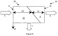
- figure 9 presents a structure of the microchip 30 where the same material 21 provides both optical gain and saturable absorption.
- a material could comprise, for example, YAG co-doped with Nd and Cr.
- An undoped end cap 3 is included to maintain an approximately constant cavity length (the sum of optical path lengths 23 and 13 ).
- the optical path length 23 of both the gain and the saturable absorber regions is increased, causing both the gain as well as the optical losses to increase.
- FIG. 10 An equivalent geometry of this embodiment example is shown in Fig. 10 .
- the combined material 21 in figure 9 has been conceptually divided in separate regions: gain medium 1 and saturable absorber 2 in figure 10 .
- the end-cap 3 is correspondingly divided into two parts 3a and 3b.
- a system for generating a laser beam with controllable peak power density, based on a wedged laser microchip and a variable focus lens, is disclosed on figure 11 .
- the microchip 30 illustrated in figure 1 is supplemented with a lens 15 whose focal length is controlled by voltage 14.
- the microchip output beam 6 passes through the lens 15, which emits a refocused beam 24.
- the control of the peak power density of the laser beam is thus facilitated in a simple, compact and inexpensive system.
- this feature is of interest for different applications.
- Combining the different embodiments described above (geometries of the wedged microlaser and pump regimes) with variable-focus optics allows independent control of different output performance parameters of the system.
- the spot size of the laser beam can be changed in order to change the area of treated material, while keeping a constant peak power in order to preserve the efficiency of the interaction.
Landscapes
- Physics & Mathematics (AREA)
- Electromagnetism (AREA)
- Engineering & Computer Science (AREA)
- Plasma & Fusion (AREA)
- Optics & Photonics (AREA)
- Lasers (AREA)
- Optical Couplings Of Light Guides (AREA)
- Semiconductor Lasers (AREA)
Claims (18)
- Un microlaser à déclenchement passif comprenant :a) une cavité monolithique résonnante (30) formée entre un premier miroir (9) et un second miroir (10) entre lesquels, en fonctionnement, est défini un trajet optique où se produit un effet laser ;b) un milieu de gain (1) disposé dans le trajet optique au sein de la cavité monolithique résonnante (30) pour produire un gain optique ;c) un milieu absorbant saturable (2) disposé dans le trajet optique au sein de la cavité monolithique résonnante (30) en communication optique et en contact physique avec le milieu de gain ; etd) un port d'entrée (5) au niveau du premier miroir (9) pour recevoir une lumière de pompage ayant une longueur d'onde de pompage pour exciter ledit milieu de gain (1) de manière à produire un faisceau laser à une longueur d'onde à effet laser qui oscille entre les premier (9) et second (10) miroirs au sein de la cavité monolithique résonnante (30) ;e) des moyens alternatifs (7) pour déplacer de façon linéaire le port d'entrée (5) par rapport à la cavité monolithique résonnante (30) le long d'une direction parallèle au premier miroir (9) ;dans lequel au moins un milieu parmi le milieu de gain (1) ou le milieu absorbateur saturable (2) est en forme de biseau ou comprend des étages discrets, moyennant quoi le mouvement transversal du port d'entrée (5) relativement à la cavité monolithique résonnante (30) cause une variation de :i) la distance (11) traversée par le faisceau laser à travers le milieu de gain (1) ;ii) la distance (12) traversée par le faisceau laser à travers le milieu absorbant saturable (2) ;dans lequel une longueur du trajet optique du faisceau laser entre les premier (9) et second (10) miroirs ne change pas lors du mouvement transversal du faisceau laser de part et d'autre du milieu de gain en forme de biseau (1) ou du milieu absorbateur saturable en forme de biseau (2), ou de part et d'autre d'un seul étage du milieu de gain à étage (1) ou du milieu absorbateur saturable à étage (2).
- Le microlaser dans la revendication 1 dans lequel le mouvement transversal de la cavité monolithique résonnante (30) est utilisé afin de contrôler au moins l'un des paramètres de performance de la sortie laser sélectionnés dans un groupe comprenant la durée d'impulsion, l'énergie d'impulsion, la puissance de crête et la densité de puissance de crête.
- Le microlaser dans la revendication 1 ou la revendication 2 dans lequel un faisceau de sortie (6) est couplé à une optique à focale variable (15) de sorte à contrôler la densité de puissance de crête d'impulsions laser émises (24).
- Le microlaser dans la revendication 1, la revendication 2 ou la revendication 3 dans lequel un milieu optiquement transparent (3) est disposé le long du faisceau laser au sein de la cavité monolithique résonnante (30) pour ajuster une longueur totale de la cavité monolithique résonnante (30).
- Le microlaser tel que défini dans n'importe laquelle des revendications 1 à 4 dans lequel le milieu absorbant saturable (2) est disposé dans une position à l'écart des premier (9) et second (10) miroirs de telle sorte que des effets de brûlage de trous spatiaux sont réduits.
- Le microlaser tel que défini dans n'importe laquelle des revendications 1 à 5 dans lequel le premier miroir (9) est hautement transmissif à la longueur d'onde de pompage et hautement réfléchissant à la longueur d'onde à effet laser.
- Le microlaser tel que défini dans n'importe laquelle des revendications 1 à 6 dans lequel le second miroir (10) est partiellement transmissif à la longueur d'onde à effet laser.
- Le microlaser tel que défini dans n'importe laquelle des revendications 1 à 7 dans lequel le milieu absorbant saturable (2) a une première et une seconde surface, toutes deux étant intersectées par le faisceau laser.
- Le microlaser dans la revendication 8 dans lequel l'une des première et seconde surfaces de milieu absorbant saturable est déviée de la perpendiculaire par rapport au faisceau laser.
- Le microlaser dans la revendication 8 dans lequel les deux surfaces de milieu absorbant saturable ne sont pas perpendiculaires par rapport au faisceau laser.
- Le microlaser dans la revendication 8 dans lequel l'une des surfaces de milieu absorbant saturable est soit planaire, soit cylindrique, soit sphérique.
- Le microlaser dans la revendication 8 dans lequel les deux surfaces de l'absorbeur saturable sont symétriques autour d'un plan perpendiculaire au trajet optique.
- Le microlaser tel que défini dans n'importe laquelle des revendications 1 à 7, dans lequel le milieu de gain (2) a une première et une seconde surface, toutes les deux étant intersectées par le faisceau laser.
- Le microlaser dans la revendication 13 dans lequel l'une des première et seconde surfaces de milieu de gain est déviée de la perpendiculaire par rapport au faisceau laser
- Le microlaser dans la revendication 13 dans lequel les deux surfaces de milieu de gain ne sont pas perpendiculaires par rapport au faisceau laser.
- Le microlaser dans la revendication 13 dans lequel l'une des surfaces de milieu de gain est soit planaire, soit cylindrique, soit sphérique.
- Le microlaser dans la revendication 13 dans lequel les deux surfaces de milieu de gain sont symétriques autour d'un plan perpendiculaire au trajet optique.
- Le microlaser tel que défini dans n'importe laquelle des revendications 1 à 8 ou 13, dans lequel le milieu absorbant saturable (2) et le milieu de gain (1) sont liés au niveau d'une interface commune (20).
Applications Claiming Priority (1)
| Application Number | Priority Date | Filing Date | Title |
|---|---|---|---|
| US71878005P | 2005-09-20 | 2005-09-20 |
Publications (2)
| Publication Number | Publication Date |
|---|---|
| EP1764886A1 EP1764886A1 (fr) | 2007-03-21 |
| EP1764886B1 true EP1764886B1 (fr) | 2016-05-04 |
Family
ID=37401000
Family Applications (2)
| Application Number | Title | Priority Date | Filing Date |
|---|---|---|---|
| EP06120955.7A Active EP1764886B1 (fr) | 2005-09-20 | 2006-09-20 | Microlaser à déclenchement passif avec densité de puissance de crête controlée |
| EP06120942A Withdrawn EP1793461A3 (fr) | 2005-09-20 | 2006-09-20 | Plateforme modulaire pour laser à l'état solide basée sur un boîtier coaxial et assemblage correspondant |
Family Applications After (1)
| Application Number | Title | Priority Date | Filing Date |
|---|---|---|---|
| EP06120942A Withdrawn EP1793461A3 (fr) | 2005-09-20 | 2006-09-20 | Plateforme modulaire pour laser à l'état solide basée sur un boîtier coaxial et assemblage correspondant |
Country Status (2)
| Country | Link |
|---|---|
| US (2) | US8031749B2 (fr) |
| EP (2) | EP1764886B1 (fr) |
Families Citing this family (26)
| Publication number | Priority date | Publication date | Assignee | Title |
|---|---|---|---|---|
| FR2916310B1 (fr) * | 2007-05-14 | 2009-08-28 | Centre Nat Rech Scient | Laser a puce pulse |
| US7924895B2 (en) * | 2007-05-23 | 2011-04-12 | Bae Systems Information And Electronic Systems Integration Inc. | Monolithic diode-pumped laser cavity |
| DE102007041531A1 (de) * | 2007-08-31 | 2009-03-05 | Robert Bosch Gmbh | Lasereinrichtung und Betriebsverfahren hierfür |
| US7817884B2 (en) * | 2007-10-30 | 2010-10-19 | Corning Incorporated | Strain-managed optical waveguide assemblies and methods of forming same |
| JP5246916B2 (ja) * | 2008-04-16 | 2013-07-24 | ギガフォトン株式会社 | Euv光発生装置におけるイオン回収装置および方法 |
| KR101018278B1 (ko) * | 2008-09-19 | 2011-03-04 | 전자부품연구원 | 파장가변 소자 패키지 |
| US8787752B2 (en) * | 2009-08-21 | 2014-07-22 | California Institute Of Technology | Systems and methods for optically powering transducers and related transducers |
| US9265136B2 (en) | 2010-02-19 | 2016-02-16 | Gigaphoton Inc. | System and method for generating extreme ultraviolet light |
| US9113540B2 (en) | 2010-02-19 | 2015-08-18 | Gigaphoton Inc. | System and method for generating extreme ultraviolet light |
| US20130208762A1 (en) * | 2012-02-14 | 2013-08-15 | Halliburton Energy Services Inc. | Suppression of Stimulated Raman Scattering |
| US9031102B2 (en) | 2012-03-01 | 2015-05-12 | California Institute Of Technology | Methods of modulating microlasers at ultralow power levels, and systems thereof |
| US9001862B2 (en) | 2012-03-09 | 2015-04-07 | Raytheon Company | Miniaturized solid-state lasing device, system and method |
| CN102751654B (zh) * | 2012-06-29 | 2013-11-06 | 西北大学 | 汇聚型光纤激光器腔内倍频器 |
| JP2015530564A (ja) | 2012-07-25 | 2015-10-15 | カリフォルニア インスティチュート オブ テクノロジー | 機能ゲート及びベース電極を有するナノピラー電界効果型及び接合型トランジスタ |
| US8883645B2 (en) | 2012-11-09 | 2014-11-11 | California Institute Of Technology | Nanopillar field-effect and junction transistors |
| US9478931B2 (en) * | 2013-02-04 | 2016-10-25 | Nlight Photonics Corporation | Method for actively controlling the optical output of a seed laser |
| US9263855B2 (en) | 2013-03-15 | 2016-02-16 | Nlight Photonics Corporation | Injection locking of gain switched diodes for spectral narrowing and jitter stabilization |
| CN114594550B (zh) * | 2013-05-22 | 2023-12-29 | 菲尼萨公司 | 光学系统中像差校正的系统的方法 |
| US10096965B2 (en) | 2014-03-13 | 2018-10-09 | Nlight, Inc. | Algorithms for rapid gating of seed suspendable pulsed fiber laser amplifiers |
| US9806488B2 (en) | 2015-06-30 | 2017-10-31 | Nlight, Inc. | Adaptive boost control for gating picosecond pulsed fiber lasers |
| DE102016106742B3 (de) * | 2015-12-18 | 2017-01-19 | Rofin-Sinar Laser Gmbh | Laservorrichtung mit einem optischen Resonator und Verfahren zum Justieren der Laservorrichtung |
| JP6926390B2 (ja) * | 2017-04-24 | 2021-08-25 | 大学共同利用機関法人自然科学研究機構 | レーザ点火装置 |
| US11482828B2 (en) * | 2019-06-28 | 2022-10-25 | Thomas James Kane | Passively Q-switched laser and laser system for ranging applications |
| CN110676680A (zh) * | 2019-09-03 | 2020-01-10 | 南京理工大学 | 用于微片激光器泵浦源输出波长控制的装置 |
| JP7394083B2 (ja) * | 2021-03-11 | 2023-12-07 | 京セラSoc株式会社 | レーザ装置 |
| CN116365348A (zh) * | 2022-12-30 | 2023-06-30 | 杭州谱育科技发展有限公司 | 被动调q脉冲能量可调固态激光器和其调节方法 |
Family Cites Families (31)
| Publication number | Priority date | Publication date | Assignee | Title |
|---|---|---|---|---|
| US4395769A (en) * | 1981-03-03 | 1983-07-26 | Bell Telephone Laboratories, Incorporated | Tunable semiconductor laser |
| US4665529A (en) * | 1986-05-19 | 1987-05-12 | Spectra-Physics, Inc. | Laser diode pumped solid state laser with miniaturized quick disconnect laser head |
| US4723257A (en) * | 1986-05-19 | 1988-02-02 | Spectra-Physics, Inc. | Laser diode pumped solid state laser with miniaturized laser head |
| US4734912A (en) * | 1986-06-06 | 1988-03-29 | Lightwave Electronics Corp. | Laser diode end pumped Nd:YAG single mode laser |
| US4953166A (en) * | 1988-02-02 | 1990-08-28 | Massachusetts Institute Of Technology | Microchip laser |
| JP3082865B2 (ja) | 1991-04-09 | 2000-08-28 | ソニー株式会社 | レーザ光発生装置 |
| US5251193A (en) * | 1991-09-24 | 1993-10-05 | Nelson Jonathan B | Solid state optical disk reader |
| IT1254887B (it) | 1992-04-17 | 1995-10-11 | Italtel Spa | Dispositivo laser |
| US5303256A (en) | 1993-03-12 | 1994-04-12 | Hughes Aircraft Company | Quasi-monolithic saturable optical element |
| JPH07131102A (ja) | 1993-10-29 | 1995-05-19 | Toshiba Corp | Qスイッチレーザ発振装置 |
| US5414724A (en) * | 1994-01-19 | 1995-05-09 | North China Research Institute Of Electro-Optics | Monolithic self Q-switched laser |
| US5394413A (en) * | 1994-02-08 | 1995-02-28 | Massachusetts Institute Of Technology | Passively Q-switched picosecond microlaser |
| US5675604A (en) * | 1995-02-07 | 1997-10-07 | The United States Of America As Represented By The Secretary Of The Air Force | Portable pumped laser system |
| US5909306A (en) * | 1996-02-23 | 1999-06-01 | President And Fellows Of Harvard College | Solid-state spectrally-pure linearly-polarized pulsed fiber amplifier laser system useful for ultraviolet radiation generation |
| DE19646072A1 (de) * | 1996-11-08 | 1998-05-14 | Daimler Benz Ag | Diodengepumpter, frequenzverdoppelter Festkörperlaser |
| DE19723269A1 (de) * | 1997-06-03 | 1998-12-10 | Heidelberger Druckmasch Ag | Festkörperlaser mit einer oder mehreren Pumplichtquellen |
| JP3211770B2 (ja) * | 1998-05-11 | 2001-09-25 | 日本電気株式会社 | 固体レーザ装置及びそれを備えた固体レーザ増幅器 |
| US6185347B1 (en) * | 1999-04-20 | 2001-02-06 | Yu Zheng | Wavelength division multiplexed coupler |
| SE9901470L (sv) * | 1999-04-23 | 2000-10-24 | Iof Ab | Optisk anordning |
| US6466593B1 (en) | 2000-01-06 | 2002-10-15 | Raytheon Company | Variable path length passive Q switch |
| US6456637B1 (en) * | 2000-05-30 | 2002-09-24 | Lucent Technologies Inc. | Waveguide lasers and optical amplifiers having enhanced thermal stability |
| US20030039274A1 (en) | 2000-06-08 | 2003-02-27 | Joseph Neev | Method and apparatus for tissue treatment and modification |
| US6842466B1 (en) | 2000-07-18 | 2005-01-11 | Nanyang Technological University | Semiconductor passive Q-switch providing variable outputs |
| US6668004B2 (en) | 2000-08-11 | 2003-12-23 | Litton Systems, Inc. | Wedge-shaped microresonator and associated microlaser assembly |
| US20020186742A1 (en) * | 2001-05-03 | 2002-12-12 | Flint Graham W. | Single mode autocoupled resonator for telecommunications |
| US6895144B2 (en) * | 2002-03-15 | 2005-05-17 | Pactonix, Inc. | Structure and method for manufacturing compact optical power monitors of highly reliable performance |
| US6922281B2 (en) * | 2002-05-03 | 2005-07-26 | Lightwaves 2020, Inc. | Erbium-doped fiber amplifier and integrated module components |
| JP2004128139A (ja) * | 2002-10-01 | 2004-04-22 | Sony Corp | レーザ光発生装置及びその製造方法 |
| US6850669B2 (en) * | 2002-10-31 | 2005-02-01 | Avanex Corporation | Package for optical filter device |
| US6898231B2 (en) * | 2002-11-21 | 2005-05-24 | Coherent, Inc. | Off-peak optical pumping of yttrium orthovanadate |
| JP3741108B2 (ja) * | 2003-03-18 | 2006-02-01 | ソニー株式会社 | レーザー発光モジュール |
-
2006
- 2006-09-18 US US11/532,697 patent/US8031749B2/en active Active
- 2006-09-19 US US11/533,000 patent/US7648290B2/en not_active Expired - Fee Related
- 2006-09-20 EP EP06120955.7A patent/EP1764886B1/fr active Active
- 2006-09-20 EP EP06120942A patent/EP1793461A3/fr not_active Withdrawn
Also Published As
| Publication number | Publication date |
|---|---|
| US20070064747A1 (en) | 2007-03-22 |
| US8031749B2 (en) | 2011-10-04 |
| EP1793461A2 (fr) | 2007-06-06 |
| EP1793461A3 (fr) | 2008-07-16 |
| US7648290B2 (en) | 2010-01-19 |
| US20070116082A1 (en) | 2007-05-24 |
| EP1764886A1 (fr) | 2007-03-21 |
Similar Documents
| Publication | Publication Date | Title |
|---|---|---|
| EP1764886B1 (fr) | Microlaser à déclenchement passif avec densité de puissance de crête controlée | |
| CN109950784B (zh) | 激光器和激光雷达 | |
| US7149231B2 (en) | Monolithic, side-pumped, passively Q-switched solid-state laser | |
| US7065121B2 (en) | Waveguide architecture, waveguide devices for laser processing and beam control, and laser processing applications | |
| US9318867B2 (en) | Laser device with Kerr effect based mode-locking and operation thereof | |
| US6738396B2 (en) | Laser based material processing methods and scalable architecture for material processing | |
| JP2770939B2 (ja) | 超コンパクトq切換マイクロレーザおよびそれに関する方法 | |
| EP1763116B1 (fr) | Laser à guide d'ondes à commande de mode | |
| US6259711B1 (en) | Laser | |
| US20030021324A1 (en) | Waveguide device with mode control and pump light confinement and method of using same | |
| US5844932A (en) | Microlaser cavity and externally controlled, passive switching, solid pulsed microlaser | |
| CN110265862B (zh) | 一种高光束质量的激光器 | |
| JP4407039B2 (ja) | 固体レーザ装置および固体レーザ装置システム | |
| US6914928B2 (en) | Diode array end pumped slab laser | |
| DK2147487T3 (en) | PULSING MICROCHIPLASES | |
| JP3211770B2 (ja) | 固体レーザ装置及びそれを備えた固体レーザ増幅器 | |
| JP3053273B2 (ja) | 半導体励起固体レーザ | |
| WO2005091447A1 (fr) | Équipement laser | |
| CN113889829A (zh) | 一种脉宽可调的被动调q激光器 | |
| CN111193168A (zh) | 可切换输出的变波长激光器 | |
| US4255718A (en) | Transversely pumped dye laser having improved conversion efficiency | |
| CN201113204Y (zh) | 一种腔内倍频微片激光器 | |
| JPH05167146A (ja) | 固体レーザ装置 | |
| CN115832857B (zh) | 一种紧凑型长脉冲泵浦叠层变频大能量调q激光器及方法 | |
| US20190006811A1 (en) | Laser device with an optical resonator and method for adjusting the laser device |
Legal Events
| Date | Code | Title | Description |
|---|---|---|---|
| PUAI | Public reference made under article 153(3) epc to a published international application that has entered the european phase |
Free format text: ORIGINAL CODE: 0009012 |
|
| AK | Designated contracting states |
Kind code of ref document: A1 Designated state(s): AT BE BG CH CY CZ DE DK EE ES FI FR GB GR HU IE IS IT LI LT LU LV MC NL PL PT RO SE SI SK TR |
|
| AX | Request for extension of the european patent |
Extension state: AL BA HR MK YU |
|
| 17P | Request for examination filed |
Effective date: 20070723 |
|
| 17Q | First examination report despatched |
Effective date: 20071008 |
|
| AKX | Designation fees paid |
Designated state(s): DE FR GB |
|
| RAP1 | Party data changed (applicant data changed or rights of an application transferred) |
Owner name: LUMENTUM OPERATIONS LLC |
|
| GRAP | Despatch of communication of intention to grant a patent |
Free format text: ORIGINAL CODE: EPIDOSNIGR1 |
|
| INTG | Intention to grant announced |
Effective date: 20151204 |
|
| GRAS | Grant fee paid |
Free format text: ORIGINAL CODE: EPIDOSNIGR3 |
|
| GRAA | (expected) grant |
Free format text: ORIGINAL CODE: 0009210 |
|
| AK | Designated contracting states |
Kind code of ref document: B1 Designated state(s): DE FR GB |
|
| REG | Reference to a national code |
Ref country code: GB Ref legal event code: FG4D |
|
| REG | Reference to a national code |
Ref country code: DE Ref legal event code: R096 Ref document number: 602006048940 Country of ref document: DE |
|
| REG | Reference to a national code |
Ref country code: FR Ref legal event code: PLFP Year of fee payment: 11 |
|
| REG | Reference to a national code |
Ref country code: DE Ref legal event code: R097 Ref document number: 602006048940 Country of ref document: DE |
|
| PLBE | No opposition filed within time limit |
Free format text: ORIGINAL CODE: 0009261 |
|
| STAA | Information on the status of an ep patent application or granted ep patent |
Free format text: STATUS: NO OPPOSITION FILED WITHIN TIME LIMIT |
|
| 26N | No opposition filed |
Effective date: 20170207 |
|
| REG | Reference to a national code |
Ref country code: FR Ref legal event code: PLFP Year of fee payment: 12 |
|
| REG | Reference to a national code |
Ref country code: FR Ref legal event code: PLFP Year of fee payment: 13 |
|
| PGFP | Annual fee paid to national office [announced via postgrant information from national office to epo] |
Ref country code: DE Payment date: 20240926 Year of fee payment: 19 |
|
| PGFP | Annual fee paid to national office [announced via postgrant information from national office to epo] |
Ref country code: GB Payment date: 20240930 Year of fee payment: 19 |
|
| PGFP | Annual fee paid to national office [announced via postgrant information from national office to epo] |
Ref country code: FR Payment date: 20240926 Year of fee payment: 19 |