EP1765002A2 - Beschichtete Waferebenen Kameramodule und dazugehörige Verfahren - Google Patents
Beschichtete Waferebenen Kameramodule und dazugehörige Verfahren Download PDFInfo
- Publication number
- EP1765002A2 EP1765002A2 EP06254623A EP06254623A EP1765002A2 EP 1765002 A2 EP1765002 A2 EP 1765002A2 EP 06254623 A EP06254623 A EP 06254623A EP 06254623 A EP06254623 A EP 06254623A EP 1765002 A2 EP1765002 A2 EP 1765002A2
- Authority
- EP
- European Patent Office
- Prior art keywords
- module
- coating
- die
- wafer level
- interposer
- Prior art date
- Legal status (The legal status is an assumption and is not a legal conclusion. Google has not performed a legal analysis and makes no representation as to the accuracy of the status listed.)
- Withdrawn
Links
Images


Classifications
-
- H—ELECTRICITY
- H04—ELECTRIC COMMUNICATION TECHNIQUE
- H04N—PICTORIAL COMMUNICATION, e.g. TELEVISION
- H04N23/00—Cameras or camera modules comprising electronic image sensors; Control thereof
- H04N23/50—Constructional details
- H04N23/54—Mounting of pick-up tubes, electronic image sensors, deviation or focusing coils
-
- H—ELECTRICITY
- H10—SEMICONDUCTOR DEVICES; ELECTRIC SOLID-STATE DEVICES NOT OTHERWISE PROVIDED FOR
- H10F—INORGANIC SEMICONDUCTOR DEVICES SENSITIVE TO INFRARED RADIATION, LIGHT, ELECTROMAGNETIC RADIATION OF SHORTER WAVELENGTH OR CORPUSCULAR RADIATION
- H10F39/00—Integrated devices, or assemblies of multiple devices, comprising at least one element covered by group H10F30/00, e.g. radiation detectors comprising photodiode arrays
- H10F39/011—Manufacture or treatment of image sensors covered by group H10F39/12
- H10F39/026—Wafer-level processing
-
- H—ELECTRICITY
- H10—SEMICONDUCTOR DEVICES; ELECTRIC SOLID-STATE DEVICES NOT OTHERWISE PROVIDED FOR
- H10F—INORGANIC SEMICONDUCTOR DEVICES SENSITIVE TO INFRARED RADIATION, LIGHT, ELECTROMAGNETIC RADIATION OF SHORTER WAVELENGTH OR CORPUSCULAR RADIATION
- H10F39/00—Integrated devices, or assemblies of multiple devices, comprising at least one element covered by group H10F30/00, e.g. radiation detectors comprising photodiode arrays
- H10F39/80—Constructional details of image sensors
- H10F39/804—Containers or encapsulations
Definitions
- the present invention relates to coated wafer level camera modules and associated methods.
- Image sensors have become ubiquitous. They are widely used in digital still cameras, cellular phones, security cameras, medical equipment, automobiles, and other applications.
- the technology used to manufacture image sensors, and in particular CMOS and CCD image sensors, has continued to advance at a great pace. For example, the demands of higher resolution, lower power consumption, and smaller devices have encouraged the further miniaturization and integration of the image sensor and associated elements.
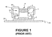
- FIG. 1 is a partially schematic cross-sectional illustration of a camera module 1 mounted to a printed circuit board 20 with a metal box 95 placed around the camera module 1 in accordance with the prior art.
- the camera module 1 includes a sensor portion 18, a lens portion 16, and a housing 3.
- the housing 3 is configured to generally prevent light from entering the camera module 1 except through an opening 4 in the housing 3.
- the camera module 1 is mounted on a socket 2.
- the metal box 95 is positioned around the camera module 1 and also carried by the socket 2.
- the socket is connected to the printed circuit board 20, connecting the camera module 1 to the circuit board 20.
- the metal box 95 is connected to a ground 93 via the socket 2 and the printed circuit board 20. Accordingly, the metal box 95 can shield the camera module 1 from selected types of electromagnetic radiation.
- the use of the socket 2 and the metal box 95 can complicate the production process. Additionally, the metal box 95 and socket 2 can increase the overall weight and size of the device, both of which can be undesirable.
- aspects of the present invention are directed toward coated wafer level camera modules and associated methods. Certain aspects of the invention are directed toward a wafer level camera module that includes a die having multiple image sensor integrated circuits.
- the module can further include at least one grounding pad and a conductive coating covering at least a portion of the die.
- the coating can be electrically coupled to the at least one grounding pad.
- the module can still further include multiple contacts that are positioned to electrically couple the integrated circuits and the at least one grounding pad to a support.
- the conductive coating can be configured to provide at least a partial shield against selected types of electromagnetic energy when the at least one grounding pad is electrically coupled to the support.
- the coating can be configured to provide at least a partial shield against one or more selected frequencies of light.
- a wafer level camera module that includes a die having multiple image sensor integrated circuits.
- the module can further include a coating covering at least a portion of the die.
- the coating can be configured to provide at least a partial shield against selected types of electromagnetic energy.
- the module can still further include multiple contacts positioned to electrically couple the integrated circuits to a support.
- the selected types of electromagnetic energy can include one or more selected frequencies of light.
- Still other aspects of the invention are directed toward a method for making a coated wafer level camera module that includes providing a wafer level camera module having a die with multiple image sensor integrated circuits, at least one grounding pad, and multiple contacts positioned to electrically couple the integrated circuits and the at least one grounding pad to a support.
- the method can further include applying a conductive coating to at least a portion of the die. The coating can be electrically coupled to the at least one grounding pad.
- Figure 1 is a partially schematic cross-sectional illustration of a camera module mounted to a printed circuit board with a metal box placed over the camera module and connected to a ground via the printed circuit board in accordance with the prior art.
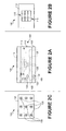
- Figure 2A is a partially schematic side view of a wafer level camera module in accordance with embodiments of the present invention.
- Figure 2B is a partially schematic top view of the wafer level camera module shown in Figure 2A.
- Figure 2C is a partially schematic bottom view of the wafer level camera module shown in Figure 2A.
- Figure 3 is a partially schematic illustration of the wafer level camera module shown in Figure 2A positioned in a chamber to receive a coating in accordance with embodiments of the present invention.
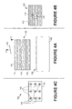
- Figure 4A is a partially schematic side view of the wafer level camera module shown in Figure 2A after having received a coating in accordance with embodiments of the present invention.
- Figure 4B is a partially schematic top view of the wafer level camera module shown in Figure 4A.
- Figure 4C is a partially schematic bottom view of the wafer level camera module shown in Figure 4A.
- Figure 5 is a partially schematic illustration of the coated wafer level camera module, shown in Figure 4A, coupled to a support in accordance with embodiments of the present invention.
- references throughout the specification to "one embodiment” or “an embodiment” means that a particular feature, structure, or characteristic described in connection with the embodiment is included in at least one embodiment of the present invention.
- the appearances of the phrase “in one embodiment” or “in an embodiment” in various places throughout the specification are not necessarily all referring to the same embodiment.
- the particular features, structures, or characteristics may be combined in any suitable manner in one or more embodiments.
- Figures 2A-5 illustrate a process for forming a coated wafer level camera module in accordance with selected embodiments of the invention.
- the coating on the module can provide at least partial shielding against selected types of electromagnetic energy.
- FIG. 2A is a partially schematic side view of a wafer level camera module 100 in accordance with embodiments of the present invention.
- the module 100 includes a die 110 having multiple image sensor integrated circuits 112.
- the image sensor integrated circuits 112 can include multiple pixels 118.
- Micro lenses 119 can be positioned over the pixels 118 and carried by the die 110 (e.g.,the micro lenses 119 can be positioned over a light sensing element of the pixel 118 and over a color filter).
- an optic assembly 116 can cover at least a portion of the pixels 118 and/or the micro lenses 119.
- the optic assembly 116 can include any number of optical devices including clear cover sheets, clear cover layers, additional lenses, optical filters, and/or the like.
- Figure 2B is a partially schematic top view of the module shown in Figure 2A.
- the die 110 can include other types of integrated circuits in addition to the image sensor integrated circuits 112. For the purposes of illustration, only nine pixels 118 are shown in Figure 2B. In other embodiments, the module 100 can include more or fewer pixels 118.
- the module 100 can also include multiple contacts 135 that are electrically coupled to the image sensor integrated circuits 112.
- the module 100 includes an interposer 105 coupled to the die 110, for example, to form a chip scale package.
- the contacts 135 are positioned on the interposer 105 to facilitate electrically coupling the integrated circuits 112 to a support (e.g., a substrate, a printed circuit board, and/or a printed wiring board).
- the contacts 135 are also shown in Figure 2C which is a partially schematic bottom view of the module shown in Figure 2A.
- the contacts 135 can include solder balls 136 that are configured or suitable for use in coupling (e.g., electrically coupling) the contacts 135 on the module 100 to pads or contacts on a support during a reflow process.
- other methods can be used to couple the contacts 135 to a support (e.g., without the use of the solder balls 136).
- the module 100 can include more or fewer contacts 135.
- the module 100 shown in Figure 2A can also includes at least one grounding pad 130.
- the module 100 includes two grounding pads 130, one on the die 110 and one on the interposer 105. In Figure 2A, both grounding pads are coupled to a contact 135 via connectors 106.
- the module 100 can include more, fewer, and/or different grounding pads 130.
- the grounding pad(s) 130 can be positioned on other portions and/or elements of the module 100. For example, in selected embodiments grounding pad(s) 130 are only located on the die 110 or only on the interposer 105.
- the grounding pad(s) 130 can be coupled to one or more contacts via other connectors 106 and/or via various portions of the integrated circuits carried by the die.
- FIG 3 is a partially schematic illustration of the wafer level camera module 100 shown in Figure 2A positioned on a stand 192 in a chamber 190 to receive a coating in accordance with embodiments of the present invention.
- a protective covering 160 has been applied to cover a portion of the optic assembly 116 and the contacts 135 (both of which are shown in Figures 2A-2C) in preparation for a coating process.
- the protective covering 160 can include any type of covering that can prevent, at least in part, the coating from adhering to a portion of the module 100 during the coating process.
- applying a protective covering 160 can include affixing a tape, affixing a film, and/or positioning an object relative to a selected portion of the module 100 to prevent, at least in part, the selected portion from being coated.
- a film has been affixed to the module 100 to cover a portion of the optic assembly 116, and the stand 192 has been positioned relative to the contacts 135 such that the contacts 135 will not be coated during the coating process.
- the protective covering 160 does not touch the object(s) it covers.
- the module 100 can include pixels 118 and/or micro lenses 119 that are recessed through an aperture in a surface of the die 110 and the protective covering 160 can cover the pixels 118 and/or micro lenses 119 without touching the pixels 118 and/or micro lenses 119 by covering the aperture.
- a coating material 170 is being introduced into the chamber via inlets 191 to cover at least a portion of the module 100 with a coating (e.g., to cover at least a portion of the die 110).
- the coating material 170 can include a single material or a number of different materials or elements introduced simultaneously or sequentially (e.g., a combination of gases that will react with one another to form a coating on the module 100).
- the materials 170 can be in various states, including in the form of a fluid (e.g., a gas, vapor, and/or liquid) and/or a solid (e.g., a powder).
- the coating process can include a vapor deposition process, a chemical deposition process, a film application process, a spray on application process, and/or an immersion process (e.g., the chamber can be filled with a coating material 170, immersing the module 100).
- the coating can be applied without the use of a chamber 190 (e.g., when using selected spray-on processes and/or when the coating includes solid film strips that are applied to the module 100).
- Figure 4A is a partially schematic side view of the module 100, shown in Figure 2A, after having received a coating 140 in accordance with embodiments of the present invention.
- the protective covering 160 has been removed from the module 100 as indicated by arrow L1, revealing an uncoated portion of the optic assembly 116 (shown in Figure 4B).
- the protective covering 160 has been removed from the contacts 135 by removing the module 100 from the 192 as indicated by arrow L2, revealing the uncoated contacts (shown in Figure 4C).
- FIG 5 is a partially schematic illustration of the coated wafer level camera module 100, shown in Figure 4A, coupled to a support 120 (e.g., a substrate, printed circuit board, and/or printed wiring board) in accordance with embodiments of the present invention.
- the contacts 135 of the module 100 can be coupled to contacts on the support 120 via various processes (e.g., using a reflow process, using a ball grid array arrangement, using flip chip technology, using bonding wires, and/or the like).
- solder balls 136 shown in Figure 2C, have been used to electrically couple the grounding pad(s) 130 and/or the integrated circuits 112 of the module 100 to the support 120 (e.g., to pads or contacts on the support 120) using a reflow process. Additionally, in selected embodiments, other portions of the module 100 can be coupled to the support using adhesives and/or other coupling methods (e.g., clips).
- the coating 140 can include a conductive coating that can be electrically coupled to the grounding pad(s) 130.
- the coating 140 can include a metal, a conductive composite (e.g., a composite having metallic fibers and/or wires) and/or a conductive plastic (e.g., a plastic having a high concentration of conductive carbon).
- the coating is conductive and has been applied so that it covers (e.g., adheres to) the grounding pad(s) 130, thereby electrically coupling the coating 140 to ground 193 via the grounding pad(s) 130, the connectors 106, the contact(s) 135, the support 120, and the connector 106 in the support.
- the coating 140 can provide at least a partial shield against selected types of electromagnetic energy 150 (e.g., electromagnetic radiation, electrical fields, and magnetic fields); thereby reducing the tendency for various types of electromagnetic energy 150 to enter and/or exit selected portions of the module 100.
- the coating 140 is conductive and electrically coupled to the ground 193, electromagnetic energy 150 that cause induced currents in conductive materials can be at least partially blocked by the coating 140 (e.g., a portion of the electromagnetic energy 150 can be converted to a current flow in the coating 140, which is electrically coupled to the ground 193).
- the coating 140 can also be configured to block (e.g., deflect or absorb) selected frequencies of electromagnetic radiation. Accordingly, the coating 140 can provide at least a partial shield against the selected frequencies of electromagnetic radiation (e.g., visual and/or infrared light) entering and/or exiting one or more portions of the module 100.
- the module 100 does not include grounding pads 130 and/or the coating 140 is not conductive, but the coating 140 is still configured to provide at least a partial shield against selected frequencies of electromagnetic radiation (e.g., frequencies falling in the light spectrum) entering and/or leaving one or more portions of the module 100.
- the coating 140 can be configured to block other types of electromagnetic energy (e.g., a radar reflective or absorbent material can be used to coat a portion of the module 100).
- a feature of some of the embodiments described above is that wafer level camera modules can be coated during the module manufacturing process, providing at least some protection against selected types of electromagnetic energy. This feature can negate the need to install a metal box around the module when assembling a device that uses the module, while still providing a selected amount of protection against electromagnetic radiation interference and/or light interference.
- An advantage of this feature is that the production complexity and/or the cost of the device can be reduced, particularly when the modules can be coated in a batch process. Additionally, because the metal box is no longer required, the size and/or the weight of the device can be reduced.
- the coating can be used to block selected frequencies of light from entering various portions of the wafer level camera module.
- the coating can be used to create a small area through which light can enter the module 100 (e.g., through the optic assembly), but can generally prevent light from entering other portions of the module 100. This can negate the need for placing a housing around the module 100 during the production process, thereby reducing complexity, size, weight, and/or cost over that of current systems.
- the wafer level camera module 100 can have other arrangements.
- the grounding pad(s) 130 are only located on the die 110 or the interposer 105, but is/are electrically coupled to a conductive coating 140 covering portions of both the die 110, the interposer 105, and the optic assembly 116.
- the module 100 does not include an interposer.
- the contacts 135 are positioned on the die 110, and the die 110 (with the contacts 135) is configured to be coupled directly to the support 120 (e.g., using direct chip attach technology).
- the coating process can also include various other arrangements.
- the protective coating(s) 160 can be applied to more, fewer, and/or other portions of the module 100 prior to the coating process.
- the module 100 does not include an optic assembly 116 and the protective covering 160 is positioned to cover an aperture associated with recessed image sensor integrated circuits 112, the micro lenses of the pixels 118, and/or other optical devices (e.g., lens(es)) associated with the image sensor integrated circuits 112.
- the protective coverings 160 are not required/used during the application of the coating 140 because one or more shaped pieces of film or tape are precisely applied to selected locations on the module 100 or because the entire module 100 is coated.
- the covering 160 can be applied to the die 110 (e.g., a die 110 with or without grounding pad(s) 130) and the die 110 can then be mounted onto an interposer 105.
- the protective cover 160 can actually be a first coating applied to selected portions of the module 100.
- a protective covering 160 in the form of a first coating can be applied to a selected area of the module (e.g., sprayed onto a portion of the optic assembly 116).
- a second coating e.g., the application of the conductive coating
- the first coating can prevent the second coating from adhering to the selected area.
- the first coating can then be removed after the second coating is applied, for example, by a solvent that will remove the first coating and/or a combination of the first and second coatings, but will not remove the first coating by itself.
Landscapes
- Engineering & Computer Science (AREA)
- Multimedia (AREA)
- Signal Processing (AREA)
- Solid State Image Pick-Up Elements (AREA)
- Studio Devices (AREA)
- Camera Bodies And Camera Details Or Accessories (AREA)
Applications Claiming Priority (1)
| Application Number | Priority Date | Filing Date | Title |
|---|---|---|---|
| US11/220,452 US20070052827A1 (en) | 2005-09-07 | 2005-09-07 | Coated wafer level camera modules and associated methods |
Publications (2)
| Publication Number | Publication Date |
|---|---|
| EP1765002A2 true EP1765002A2 (de) | 2007-03-21 |
| EP1765002A3 EP1765002A3 (de) | 2009-12-30 |
Family
ID=37700408
Family Applications (1)
| Application Number | Title | Priority Date | Filing Date |
|---|---|---|---|
| EP06254623A Withdrawn EP1765002A3 (de) | 2005-09-07 | 2006-09-05 | Beschichtete Waferebenen Kameramodule und dazugehörige Verfahren |
Country Status (4)
| Country | Link |
|---|---|
| US (1) | US20070052827A1 (de) |
| EP (1) | EP1765002A3 (de) |
| CN (1) | CN1917224B (de) |
| TW (1) | TW200739871A (de) |
Cited By (1)
| Publication number | Priority date | Publication date | Assignee | Title |
|---|---|---|---|---|
| WO2010066332A1 (de) * | 2008-12-12 | 2010-06-17 | Daimler Ag | Vorrichtung zur überwachung einer umgebung eines fahrzeugs |
Families Citing this family (21)
| Publication number | Priority date | Publication date | Assignee | Title |
|---|---|---|---|---|
| US7751594B2 (en) | 2003-04-04 | 2010-07-06 | Lumidigm, Inc. | White-light spectral biometric sensors |
| US7460696B2 (en) * | 2004-06-01 | 2008-12-02 | Lumidigm, Inc. | Multispectral imaging biometrics |
| US8229185B2 (en) * | 2004-06-01 | 2012-07-24 | Lumidigm, Inc. | Hygienic biometric sensors |
| US8787630B2 (en) * | 2004-08-11 | 2014-07-22 | Lumidigm, Inc. | Multispectral barcode imaging |
| US8175346B2 (en) * | 2006-07-19 | 2012-05-08 | Lumidigm, Inc. | Whole-hand multispectral biometric imaging |
| US8355545B2 (en) * | 2007-04-10 | 2013-01-15 | Lumidigm, Inc. | Biometric detection using spatial, temporal, and/or spectral techniques |
| US7995808B2 (en) | 2006-07-19 | 2011-08-09 | Lumidigm, Inc. | Contactless multispectral biometric capture |
| US7679167B2 (en) * | 2007-01-08 | 2010-03-16 | Visera Technologies Company, Limited | Electronic assembly for image sensor device and fabrication method thereof |
| KR101484566B1 (ko) * | 2007-03-21 | 2015-01-20 | 루미다임 인크. | 국소적으로 일관된 피처를 기초로 하는 생체인식 |
| CN101843020B (zh) * | 2007-06-11 | 2014-05-14 | 路迈蒂姆公司 | 非接触型多谱生物测量获取 |
| US20090152659A1 (en) * | 2007-12-18 | 2009-06-18 | Jari Hiltunen | Reflowable camera module with improved reliability of solder connections |
| US20090206431A1 (en) * | 2008-02-20 | 2009-08-20 | Micron Technology, Inc. | Imager wafer level module and method of fabrication and use |
| US20090243051A1 (en) * | 2008-03-28 | 2009-10-01 | Micron Technology, Inc. | Integrated conductive shield for microelectronic device assemblies and associated methods |
| US20100246902A1 (en) * | 2009-02-26 | 2010-09-30 | Lumidigm, Inc. | Method and apparatus to combine biometric sensing and other functionality |
| EP2261977A1 (de) | 2009-06-08 | 2010-12-15 | STMicroelectronics (Grenoble) SAS | Kameramodul und sein Herstellungsverfahren |
| US8872908B2 (en) * | 2009-08-26 | 2014-10-28 | Lumidigm, Inc | Dual-imager biometric sensor |
| US8570149B2 (en) | 2010-03-16 | 2013-10-29 | Lumidigm, Inc. | Biometric imaging using an optical adaptive interface |
| US8576574B2 (en) | 2010-04-21 | 2013-11-05 | Stmicroelectronics Pte Ltd. | Electromagnetic interference shielding on semiconductor devices |
| US8642119B2 (en) * | 2010-09-22 | 2014-02-04 | Stmicroelectronics Pte Ltd. | Method and system for shielding semiconductor devices from light |
| JP2012238687A (ja) * | 2011-05-11 | 2012-12-06 | Sony Corp | 半導体パッケージ、半導体装置の製造方法、および固体撮像装置 |
| EP3319125B1 (de) | 2016-11-03 | 2021-04-07 | ams AG | Verfahren zur herstellung von anordnungen optischer sensoren und gehäuse für einen optischen sensor |
Family Cites Families (13)
| Publication number | Priority date | Publication date | Assignee | Title |
|---|---|---|---|---|
| JPH01183847A (ja) * | 1988-01-19 | 1989-07-21 | Ricoh Co Ltd | 等倍イメージセンサー |
| JP3948111B2 (ja) * | 1998-04-20 | 2007-07-25 | ソニー株式会社 | ビデオカメラ |
| US6956610B1 (en) * | 1999-02-18 | 2005-10-18 | Linvatec Corporation | Shock mounting system for CCD camera |
| CN1221983C (zh) * | 2000-04-17 | 2005-10-05 | 韦吾泽罗公司 | 电缆和电缆连接器的电磁干扰屏蔽 |
| US6927379B2 (en) * | 2000-12-22 | 2005-08-09 | Ge Medical Systems Global Technology Company, Llc | Hermetically sealed digital detector |
| FR2824953B1 (fr) * | 2001-05-18 | 2004-07-16 | St Microelectronics Sa | Boitier semi-conducteur optique a lentille incorporee et blindage |
| JP2003318585A (ja) * | 2002-04-24 | 2003-11-07 | Toshiba Corp | 電子機器 |
| US7324148B2 (en) * | 2002-04-26 | 2008-01-29 | Olympus Optical Co., Ltd. | Camera and image pickup device unit used therefor having a sealing structure between a dust proofing member and an image pick up device |
| JP2004104078A (ja) * | 2002-06-28 | 2004-04-02 | Sanyo Electric Co Ltd | カメラモジュールおよびその製造方法 |
| US7329861B2 (en) * | 2003-10-14 | 2008-02-12 | Micron Technology, Inc. | Integrally packaged imaging module |
| DE102004001698A1 (de) * | 2004-01-13 | 2005-08-11 | Robert Bosch Gmbh | Optisches Modul |
| JP2005348275A (ja) * | 2004-06-04 | 2005-12-15 | Sharp Corp | 撮像素子およびカメラモジュール |
| US7279782B2 (en) * | 2005-01-05 | 2007-10-09 | Advanced Chip Engineering Technology Inc. | FBGA and COB package structure for image sensor |
-
2005
- 2005-09-07 US US11/220,452 patent/US20070052827A1/en not_active Abandoned
-
2006
- 2006-08-24 TW TW095131159A patent/TW200739871A/zh unknown
- 2006-09-05 EP EP06254623A patent/EP1765002A3/de not_active Withdrawn
- 2006-09-07 CN CN200610129193.6A patent/CN1917224B/zh active Active
Cited By (1)
| Publication number | Priority date | Publication date | Assignee | Title |
|---|---|---|---|---|
| WO2010066332A1 (de) * | 2008-12-12 | 2010-06-17 | Daimler Ag | Vorrichtung zur überwachung einer umgebung eines fahrzeugs |
Also Published As
| Publication number | Publication date |
|---|---|
| CN1917224B (zh) | 2010-09-29 |
| CN1917224A (zh) | 2007-02-21 |
| TW200739871A (en) | 2007-10-16 |
| US20070052827A1 (en) | 2007-03-08 |
| EP1765002A3 (de) | 2009-12-30 |
Similar Documents
| Publication | Publication Date | Title |
|---|---|---|
| EP1765002A2 (de) | Beschichtete Waferebenen Kameramodule und dazugehörige Verfahren | |
| KR100903824B1 (ko) | 화상센서소자용 전기적인 조립체 및 그 제조방법 | |
| US7829966B2 (en) | Electronic assembly for image sensor device | |
| US8576574B2 (en) | Electromagnetic interference shielding on semiconductor devices | |
| US8251601B2 (en) | Camera module and method for fabricating the same | |
| US8642119B2 (en) | Method and system for shielding semiconductor devices from light | |
| US8139145B2 (en) | Camera module | |
| US7720374B2 (en) | Camera module | |
| US8351219B2 (en) | Electronic assembly for an image sensing device | |
| KR100959922B1 (ko) | 카메라 모듈 및 그 제조방법 | |
| US7928538B2 (en) | Package-level electromagnetic interference shielding | |
| TWI496462B (zh) | 用於相機模組之電磁干擾屏蔽 | |
| US7659134B2 (en) | Microelectronic imagers and methods for manufacturing such microelectronic imagers | |
| US9099368B2 (en) | Electromagnetic shielding for camera modules | |
| US9419047B2 (en) | Image sensor device with aligned IR filter and dielectric layer and related methods | |
| CN1453866A (zh) | 电子器件 | |
| JP2008512851A (ja) | ウエハー水準でカメラモジュールを製造する方法 | |
| US20070210246A1 (en) | Stacked image sensor optical module and fabrication method | |
| US9525832B1 (en) | Image sensor device with an electromagnetic compatibility shield (EMC) and associated methods | |
| US20130140664A1 (en) | Flip chip packaging structure | |
| US20160104737A1 (en) | Image sensor device with flexible interconnect layer and related methods | |
| CN209086962U (zh) | 用于屏下光学指纹的识别组件及电子设备 | |
| US20040070076A1 (en) | Semiconductor chip package for image sensor and method of the same | |
| KR20150025831A (ko) | 이미지 센서 칩 패키지 및 이를 구비하는 이미지 센서 모듈 | |
| JP2004221874A (ja) | 光モジュール及びその製造方法、回路基板並びに電子機器 |
Legal Events
| Date | Code | Title | Description |
|---|---|---|---|
| PUAI | Public reference made under article 153(3) epc to a published international application that has entered the european phase |
Free format text: ORIGINAL CODE: 0009012 |
|
| 17P | Request for examination filed |
Effective date: 20060925 |
|
| AK | Designated contracting states |
Kind code of ref document: A2 Designated state(s): AT BE BG CH CY CZ DE DK EE ES FI FR GB GR HU IE IS IT LI LT LU LV MC NL PL PT RO SE SI SK TR |
|
| AX | Request for extension of the european patent |
Extension state: AL BA HR MK YU |
|
| PUAL | Search report despatched |
Free format text: ORIGINAL CODE: 0009013 |
|
| AK | Designated contracting states |
Kind code of ref document: A3 Designated state(s): AT BE BG CH CY CZ DE DK EE ES FI FR GB GR HU IE IS IT LI LT LU LV MC NL PL PT RO SE SI SK TR |
|
| AX | Request for extension of the european patent |
Extension state: AL BA HR MK RS |
|
| AKX | Designation fees paid |
Designated state(s): AT BE BG CH CY CZ DE DK EE ES FI FR GB GR HU IE IS IT LI LT LU LV MC NL PL PT RO SE SI SK TR |
|
| STAA | Information on the status of an ep patent application or granted ep patent |
Free format text: STATUS: THE APPLICATION IS DEEMED TO BE WITHDRAWN |
|
| 18D | Application deemed to be withdrawn |
Effective date: 20100401 |