EP1768093A2 - Dispositif électroluminescent et son procédé de commande - Google Patents
Dispositif électroluminescent et son procédé de commande Download PDFInfo
- Publication number
- EP1768093A2 EP1768093A2 EP06011078A EP06011078A EP1768093A2 EP 1768093 A2 EP1768093 A2 EP 1768093A2 EP 06011078 A EP06011078 A EP 06011078A EP 06011078 A EP06011078 A EP 06011078A EP 1768093 A2 EP1768093 A2 EP 1768093A2
- Authority
- EP
- European Patent Office
- Prior art keywords
- scan
- data
- current
- lines
- light emitting
- Prior art date
- Legal status (The legal status is an assumption and is not a legal conclusion. Google has not performed a legal analysis and makes no representation as to the accuracy of the status listed.)
- Granted
Links
Images


Classifications
-
- G—PHYSICS
- G09—EDUCATION; CRYPTOGRAPHY; DISPLAY; ADVERTISING; SEALS
- G09G—ARRANGEMENTS OR CIRCUITS FOR CONTROL OF INDICATING DEVICES USING STATIC MEANS TO PRESENT VARIABLE INFORMATION
- G09G3/00—Control arrangements or circuits, of interest only in connection with visual indicators other than cathode-ray tubes
- G09G3/20—Control arrangements or circuits, of interest only in connection with visual indicators other than cathode-ray tubes for presentation of an assembly of a number of characters, e.g. a page, by composing the assembly by combination of individual elements arranged in a matrix no fixed position being assigned to or needed to be assigned to the individual characters or partial characters
- G09G3/22—Control arrangements or circuits, of interest only in connection with visual indicators other than cathode-ray tubes for presentation of an assembly of a number of characters, e.g. a page, by composing the assembly by combination of individual elements arranged in a matrix no fixed position being assigned to or needed to be assigned to the individual characters or partial characters using controlled light sources
- G09G3/30—Control arrangements or circuits, of interest only in connection with visual indicators other than cathode-ray tubes for presentation of an assembly of a number of characters, e.g. a page, by composing the assembly by combination of individual elements arranged in a matrix no fixed position being assigned to or needed to be assigned to the individual characters or partial characters using controlled light sources using electroluminescent panels
- G09G3/32—Control arrangements or circuits, of interest only in connection with visual indicators other than cathode-ray tubes for presentation of an assembly of a number of characters, e.g. a page, by composing the assembly by combination of individual elements arranged in a matrix no fixed position being assigned to or needed to be assigned to the individual characters or partial characters using controlled light sources using electroluminescent panels semiconductive, e.g. using light-emitting diodes [LED]
- G09G3/3208—Control arrangements or circuits, of interest only in connection with visual indicators other than cathode-ray tubes for presentation of an assembly of a number of characters, e.g. a page, by composing the assembly by combination of individual elements arranged in a matrix no fixed position being assigned to or needed to be assigned to the individual characters or partial characters using controlled light sources using electroluminescent panels semiconductive, e.g. using light-emitting diodes [LED] organic, e.g. using organic light-emitting diodes [OLED]
- G09G3/3216—Control arrangements or circuits, of interest only in connection with visual indicators other than cathode-ray tubes for presentation of an assembly of a number of characters, e.g. a page, by composing the assembly by combination of individual elements arranged in a matrix no fixed position being assigned to or needed to be assigned to the individual characters or partial characters using controlled light sources using electroluminescent panels semiconductive, e.g. using light-emitting diodes [LED] organic, e.g. using organic light-emitting diodes [OLED] using a passive matrix
-
- G—PHYSICS
- G09—EDUCATION; CRYPTOGRAPHY; DISPLAY; ADVERTISING; SEALS
- G09G—ARRANGEMENTS OR CIRCUITS FOR CONTROL OF INDICATING DEVICES USING STATIC MEANS TO PRESENT VARIABLE INFORMATION
- G09G3/00—Control arrangements or circuits, of interest only in connection with visual indicators other than cathode-ray tubes
- G09G3/20—Control arrangements or circuits, of interest only in connection with visual indicators other than cathode-ray tubes for presentation of an assembly of a number of characters, e.g. a page, by composing the assembly by combination of individual elements arranged in a matrix no fixed position being assigned to or needed to be assigned to the individual characters or partial characters
- G09G3/22—Control arrangements or circuits, of interest only in connection with visual indicators other than cathode-ray tubes for presentation of an assembly of a number of characters, e.g. a page, by composing the assembly by combination of individual elements arranged in a matrix no fixed position being assigned to or needed to be assigned to the individual characters or partial characters using controlled light sources
- G09G3/30—Control arrangements or circuits, of interest only in connection with visual indicators other than cathode-ray tubes for presentation of an assembly of a number of characters, e.g. a page, by composing the assembly by combination of individual elements arranged in a matrix no fixed position being assigned to or needed to be assigned to the individual characters or partial characters using controlled light sources using electroluminescent panels
- G09G3/32—Control arrangements or circuits, of interest only in connection with visual indicators other than cathode-ray tubes for presentation of an assembly of a number of characters, e.g. a page, by composing the assembly by combination of individual elements arranged in a matrix no fixed position being assigned to or needed to be assigned to the individual characters or partial characters using controlled light sources using electroluminescent panels semiconductive, e.g. using light-emitting diodes [LED]
- G09G3/3208—Control arrangements or circuits, of interest only in connection with visual indicators other than cathode-ray tubes for presentation of an assembly of a number of characters, e.g. a page, by composing the assembly by combination of individual elements arranged in a matrix no fixed position being assigned to or needed to be assigned to the individual characters or partial characters using controlled light sources using electroluminescent panels semiconductive, e.g. using light-emitting diodes [LED] organic, e.g. using organic light-emitting diodes [OLED]
- G09G3/3275—Details of drivers for data electrodes
- G09G3/3283—Details of drivers for data electrodes in which the data driver supplies a variable data current for setting the current through, or the voltage across, the light-emitting elements
-
- G—PHYSICS
- G09—EDUCATION; CRYPTOGRAPHY; DISPLAY; ADVERTISING; SEALS
- G09G—ARRANGEMENTS OR CIRCUITS FOR CONTROL OF INDICATING DEVICES USING STATIC MEANS TO PRESENT VARIABLE INFORMATION
- G09G2300/00—Aspects of the constitution of display devices
- G09G2300/04—Structural and physical details of display devices
- G09G2300/0421—Structural details of the set of electrodes
- G09G2300/043—Compensation electrodes or other additional electrodes in matrix displays related to distortions or compensation signals, e.g. for modifying TFT threshold voltage in column driver
-
- G—PHYSICS
- G09—EDUCATION; CRYPTOGRAPHY; DISPLAY; ADVERTISING; SEALS
- G09G—ARRANGEMENTS OR CIRCUITS FOR CONTROL OF INDICATING DEVICES USING STATIC MEANS TO PRESENT VARIABLE INFORMATION
- G09G2300/00—Aspects of the constitution of display devices
- G09G2300/06—Passive matrix structure, i.e. with direct application of both column and row voltages to the light emitting or modulating elements, other than LCD or OLED
-
- G—PHYSICS
- G09—EDUCATION; CRYPTOGRAPHY; DISPLAY; ADVERTISING; SEALS
- G09G—ARRANGEMENTS OR CIRCUITS FOR CONTROL OF INDICATING DEVICES USING STATIC MEANS TO PRESENT VARIABLE INFORMATION
- G09G2320/00—Control of display operating conditions
- G09G2320/02—Improving the quality of display appearance
- G09G2320/0209—Crosstalk reduction, i.e. to reduce direct or indirect influences of signals directed to a certain pixel of the displayed image on other pixels of said image, inclusive of influences affecting pixels in different frames or fields or sub-images which constitute a same image, e.g. left and right images of a stereoscopic display
-
- G—PHYSICS
- G09—EDUCATION; CRYPTOGRAPHY; DISPLAY; ADVERTISING; SEALS
- G09G—ARRANGEMENTS OR CIRCUITS FOR CONTROL OF INDICATING DEVICES USING STATIC MEANS TO PRESENT VARIABLE INFORMATION
- G09G2320/00—Control of display operating conditions
- G09G2320/02—Improving the quality of display appearance
- G09G2320/0223—Compensation for problems related to R-C delay and attenuation in electrodes of matrix panels, e.g. in gate electrodes or on-substrate video signal electrodes
-
- G—PHYSICS
- G09—EDUCATION; CRYPTOGRAPHY; DISPLAY; ADVERTISING; SEALS
- G09G—ARRANGEMENTS OR CIRCUITS FOR CONTROL OF INDICATING DEVICES USING STATIC MEANS TO PRESENT VARIABLE INFORMATION
- G09G2320/00—Control of display operating conditions
- G09G2320/02—Improving the quality of display appearance
- G09G2320/0233—Improving the luminance or brightness uniformity across the screen
-
- G—PHYSICS
- G09—EDUCATION; CRYPTOGRAPHY; DISPLAY; ADVERTISING; SEALS
- G09G—ARRANGEMENTS OR CIRCUITS FOR CONTROL OF INDICATING DEVICES USING STATIC MEANS TO PRESENT VARIABLE INFORMATION
- G09G3/00—Control arrangements or circuits, of interest only in connection with visual indicators other than cathode-ray tubes
- G09G3/20—Control arrangements or circuits, of interest only in connection with visual indicators other than cathode-ray tubes for presentation of an assembly of a number of characters, e.g. a page, by composing the assembly by combination of individual elements arranged in a matrix no fixed position being assigned to or needed to be assigned to the individual characters or partial characters
- G09G3/22—Control arrangements or circuits, of interest only in connection with visual indicators other than cathode-ray tubes for presentation of an assembly of a number of characters, e.g. a page, by composing the assembly by combination of individual elements arranged in a matrix no fixed position being assigned to or needed to be assigned to the individual characters or partial characters using controlled light sources
- G09G3/30—Control arrangements or circuits, of interest only in connection with visual indicators other than cathode-ray tubes for presentation of an assembly of a number of characters, e.g. a page, by composing the assembly by combination of individual elements arranged in a matrix no fixed position being assigned to or needed to be assigned to the individual characters or partial characters using controlled light sources using electroluminescent panels
- G09G3/32—Control arrangements or circuits, of interest only in connection with visual indicators other than cathode-ray tubes for presentation of an assembly of a number of characters, e.g. a page, by composing the assembly by combination of individual elements arranged in a matrix no fixed position being assigned to or needed to be assigned to the individual characters or partial characters using controlled light sources using electroluminescent panels semiconductive, e.g. using light-emitting diodes [LED]
- G09G3/3208—Control arrangements or circuits, of interest only in connection with visual indicators other than cathode-ray tubes for presentation of an assembly of a number of characters, e.g. a page, by composing the assembly by combination of individual elements arranged in a matrix no fixed position being assigned to or needed to be assigned to the individual characters or partial characters using controlled light sources using electroluminescent panels semiconductive, e.g. using light-emitting diodes [LED] organic, e.g. using organic light-emitting diodes [OLED]
- G09G3/3266—Details of drivers for scan electrodes
Definitions
- the present invention relates to a light emitting device and a method of driving the same. More particularly, the present invention relates to a light emitting device where currents passing through scan lines have the same values and a method of driving the same.
- a light emitting device emits a light having a certain wavelength, and especially an organic electroluminescent device is self light emitting device.
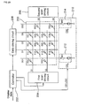
- FIG. 1A is a block diagram illustrating a common organic electroluminescent device.
- FIG. 1B and FIG. 1C are views illustrating a method of driving the organic electroluminescent device of FIG. 1A.
- the organic electroluminescent device includes a panel 100, a controller 102, a first scan driving circuit 104, a second scan driving circuit 106 and a data driving circuit 108.
- the panel 100 includes a plurality of pixels E11 to E34 formed in cross areas of data lines D1 to D3 and scan lines S1 to S4.
- the controller 102 controls the scan driving circuits 104 and 106 and the data driving circuit 108 by using display data inputted from an outside apparatus (not shown).
- the first scan driving circuit 104 is coupled to some of the scan lines S1 to S4, e.g. S1 and S3, and transmits first scan signals to the some S1 and S3.
- the second scan driving circuit 106 is coupled to the other scan lines S2 and S4, and transmits second scan signals to the other scan lines S2 and S4.
- the data driving circuit 108 provides data currents corresponding to the display data to the data lines D1 to D3 under control of the controller 102, and so the pixels E11 to E34 emit a light.
- the pixels E11 to E34 emit a light when corresponding scan line is coupled to a ground, and do not emit a light when corresponding scan line is coupled to a non-luminescent source having the same magnitude as a driving voltage of the organic electroluminescent device, e.g. a voltage V1 corresponding to maximum brightness of pixel.
- a driving voltage of the organic electroluminescent device e.g. a voltage V1 corresponding to maximum brightness of pixel.
- data current of 0A is provided to a pixel E11 through a first data line D1
- data currents of 3A are provided to the other pixels E12 to E34.
- resistor hereinafter, referred to as "scan line resistor" which each of the scan lines S1 to S4 has is assumed by 10 ⁇ .
- the first scan line S1 is coupled to the ground, and the second to fourth scan lines S2 to S4 are coupled to the non-luminescent source. Accordingly, pixels E21 and E31 of the pixels E11 to E31 corresponding to the first scan line S1 emit a light. In this case, a first current passing to the ground through the first scan line S1 is 6A. Hence, each of cathode voltages VC21 and VC31 of the pixels E21 and E31 is 60V (scan line resistor ⁇ 6A).
- the second scan line S2 is coupled to the ground, and the first, third and fourth scan lines S1, S3 and S4 are coupled to the non-luminescent source. Accordingly, pixels E12 to E32 corresponding to the second scan line S2 emit a light. In this case, a second current passing to the ground through the second scan line S2 is 9A. Hence, each of cathode voltages VC12 to VC32 of the pixels E12 to E32 is 90V (scan line resistor ⁇ 9A).
- the pixel E21 corresponding to the first scan line S1 and the pixel E22 corresponding to the second scan line S2 will be compared.
- the cathode voltage VC21 and VC22 of the pixels E21 and E22 have different magnitude.
- the brightness of a pixel is affected by cathode voltage of the pixel, and thus the pixels E21 and E22 emit light having different brightness.
- the higher cathode voltage of a pixel has magnitude, the lower the pixel has brightness. Accordingly, the pixel E21 emits a light having higher brightness than the pixel E22.
- the cathode voltages VC31 and VC32 of the pixels E31 and E32 are different magnitude, and so the pixels E31 and E32 emit light having different brightness. This is referred to as "cross-talk phenomenon".
- a light emitting device includes data lines, scan lines, pixels, one or more dummy data line and a cross-talk preventing circuit.
- the data lines are disposed in a first direction, and the scan lines are disposed in a second direction different from the first direction.
- the pixels are formed in cross areas of the data lines and the scan lines.
- the dummy data line is disposed in the first direction.
- the cross-talk preventing circuit provides a compensating current to scan line related to luminescence of the scan lines through the dummy data line so that total sum of current passing through the scan line has a desired value.
- An organic electroluminescent device includes data lines, at least one dummy data line, scan lines, a plurality of pixels, a plurality of dummy pixels and a cross-talk preventing circuit.
- the data lines are disposed in a first direction.
- the dummy data line is disposed in the first direction outside of outmost data line of the data lines.
- the scan lines are disposed in a second direction different from the first direction.
- the pixels are formed in cross areas of the data lines and the scan lines.
- the dummy pixels are formed in cross areas of the dummy data line and the scan lines.
- the cross-talk preventing circuit provides compensating currents to each of the scan lines through the dummy data lines. Here, currents passing through each of the scan lines have the same values.
- a method of driving a light emitting device having a plurality of pixels formed in cross areas of data lines and scan lines includes receiving a plurality of display data; providing data currents corresponding to one display data of the received display data to the data lines; and providing a compensating current to a scan line related to luminescence of the scan lines so that total sum of current passing through the scan line has a desired value.
- FIG. 1A is a block diagram illustrating a common organic electroluminescent device
- FIG. 1B and FIG. 1C are views illustrating a method of driving the organic electroluminescent device of FIG. 1A;
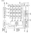
- FIG. 2A is a block diagram illustrating a light emitting device according to a first embodiment of the present invention
- Fig. 2B is a sectional view illustrating one pixel in FIG. 2A;
- FIG. 2C and FIG. 2D are views illustrating a process of driving the light emitting device of FIG. 2A;
- FIG 3 is a block diagram illustrating a light emitting device according to a second embodiment of the present invention.
- FIG. 4 is a view illustrating a light emitting device according to a third embodiment of the present invention.
- FIG. 5A is a view illustrating a light emitting device according to a fourth embodiment of the present invention.
- FIG. 5B is a view illustrating a process of driving the light emitting device of FIG. 5A.
- FIG. 6 is a view illustrating a light emitting device according to a fifth embodiment of the present invention.
- FIG. 2A is a block diagram illustrating a light emitting device according to a first embodiment of the present invention.
- Fig. 2B is a sectional view illustrating one pixel in FIG. 2A.
- FIG. 2C and FIG. 2D are views illustrating a process of driving the light emitting device of FIG. 2A.
- the light emitting device of the present invention includes a panel 200, a controller 202, a first scan driving circuit 204, a second scan driving circuit 206, a data driving circuit 208 and a cross-talk preventing circuit 210.
- the light emitting device includes an organic electroluminescent device, a plasma display panel, a liquid crystal display, and others.
- the organic electroluminescent device will be described as an example of the light emitting device for convenience of the description.
- the panel 200 includes a plurality of pixels E11 to E34 formed in cross areas of data lines D1 to D3 and scan lines S1 to S4 and dummy pixels DE1 to DE4 formed in cross areas of dummy data lines DD1 and DD2 and the scan lines S1 to S4.
- each of the pixels E11 to E34 has an anode electrode layer 222 as transparent electrode, an organic layer 224 made up of organic substance and a cathode electrode layer 226 made up of metal such as aluminum Al, etc. formed in sequence on a substrate 220.
- the organic layer 224 includes an emitting layer.
- the organic layer 224 emits a light having a certain wavelength.
- the controller 202 controls the scan driving circuits 204 and 206, the data driving circuit 208 and the cross-talk preventing circuit 210 by using display data, e.g. RGB data inputted from an outside apparatus (not shown).
- display data e.g. RGB data inputted from an outside apparatus (not shown).
- the controller 202 may store the display data.
- the first scan driving circuit 204 is coupled to some of the scan lines S1 to S4, e.g. S1 and S3, and transmits first scan signals to the some S1 and S3.
- the second scan driving circuit 206 is coupled to the other scan lines S2 and S4, and transmits second scan lines to the other scan lines S2 and S4.
- the data driving circuit 208 provides data currents corresponding to the display data to the data lines D1 to D3 under control of the controller 202, and so the pixels E11 to E34 emit light.
- the data currents are synchronized with the scan signals.
- the cross-talk preventing circuit 210 includes a first current providing circuit 212 and a second current providing circuit 214.
- the first current providing circuit 212 includes a first current source, and provides a first current outputted from the first current source to the scan lines S1 and S3 in accordance with a first controlling signal CS1 transmitted from the controller 202.
- the second current providing circuit 214 includes a second current source, and provides a second current outputted from the second current source to the other scan lines S2 and S4 in accordance with a second controlling signal CS2 transmitted from the controller 202.
- the current providing circuits 212 and 214 provide the first and second currents to the scan lines S1 to S4 so that current passing through the scan lines S1 to S4 have the same values.
- the pixels E11 to E34 emit a light when corresponding scan line is coupled to a luminescent source, preferably ground, and do not emit a light when corresponding scan line is coupled to a non-luminescent source having the same magnitude as a driving voltage of the light emitting device, e.g. a voltage V2 corresponding to maximum brightness of pixel.
- a driving voltage of the light emitting device e.g. a voltage V2 corresponding to maximum brightness of pixel.
- data current of 0A is provided to a pixel E11 through a first data line D1
- data currents of 3A are provided to the other pixels E12 to E34.
- resistor hereinafter, referred to as "scan line resistor which each of the scan lines S1 to S4 has is assumed by 10 ⁇ .
- the luminescent source is assumed to be the ground.
- the controller 202 analyzes first display data inputted from the outside apparatus, and so detects that current passing through the first scan line S1 is 6A. Then, the controller 202 transmits a first controlling signal CS1 to the first current providing circuit 212.
- the first scan line S1 is coupled to the ground, and the second to fourth scan lines S2 to S4 are coupled to the non-luminescent source.
- the first current providing circuit 212 provides dummy data current of 4A to the first scan line S1 through the first dummy data line DD1 and the first dummy pixel DE1 after tuming-on a switch SW1 in accordance with the first controlling signal CS1.
- current of 10A passes to the ground through the first scan line S1.
- cathode voltages VC11 to VC31 of the pixels E11 to E31 corresponding to the first scan line S1 are 100V (10A ⁇ 10 ⁇ ).
- the controller 202 analyzes second display data inputted from the outside apparatus, and so detects that current passing through the second scan line S2 is 9A. Then, the controller 202 transmits a second controlling signal CS2 to the second current providing circuit 214.
- the second display data is inputted to the controller 202 after the first display data is inputted to the controller 202.
- the second scan line S2 is coupled to the ground, and the first, third and fourth scan lines S1, S3 and S4 are coupled to the non-luminescent source.
- the second current providing circuit 214 provides dummy data current of 1A to the second scan line S2 through the second dummy data line DD2 and the second dummy pixel DE2 after tuming-on a switch SW2 in accordance with the second controlling signal CS2.
- current of 10A passes to the ground through the second scan line S2.
- cathode voltages VC12 to VC32 of the pixels E12 to E32 corresponding to the second scan line S2 are 100V (10A ⁇ 10 ⁇ ).
- Cathode voltages VC13 to E34 of the pixels E13 to E34 corresponding to the third and fourth scan lines S3 and S4 calculated by using the above method are 100V (10A ⁇ 10 ⁇ ).
- the cathode voltages of the pixels E11 to E34 have the same magnitude irrespective of the magnitude of the data currents provided to the data lines D1 to D3. Therefore, in the light emitting device of the present invention unlike the light emitting device described in Related Art, the pixels have the same brightness when data currents having the same magnitude are provided to the pixels. Accordingly, in the light emitting device of the present invention unlike the light emitting device described in Related Art, a cross-talk phenomenon is not occurred.
- FIG 3 is a block diagram illustrating a light emitting device according to a second embodiment of the present invention.
- the light emitting device of the present invention includes a panel 300, a controller 302, a first scan driving circuit 304, a second scan driving circuit 306, a data driving circuit 308 and a cross-talk preventing circuit 310.
- the cross-talk preventing circuit 310 includes a first current providing circuit 312 and a second current providing circuit 314.
- the first current providing circuit 312 provides a certain current to some of the scan lines S1 to S4. e.g. S1 and S3 using a first OP amplifier included therein so that the currents passing through the scan lines S1 to S4 have the same values.
- the first current providing circuit 312 will be described through the first scan line S1.
- value of current passing through each of the scan lines S1 to S4 by using the first OP amplifier is assumed by 10A.
- the cathode voltage of a dummy pixel DE11 is assumed by 100V.
- An input voltage V2 corresponding to the value of the current is inputted to one terminal of input terminals of the first OP amplifier. Additionally, the other terminal of the input terminals is coupled to a dummy pixel DE21, and so the first current providing circuit 312 detects cathode voltage of the dummy pixel DE21.
- the first OP amplifier provides a certain current to the first scan line S1 through a first dummy data line DD1 and the dummy pixel DE11 so that the cathode voltage of the dummy pixel DE11 is 100V.
- the first OP amplifier does not output any current.
- the second current providing circuit 314 provides a certain current to the other scan lines by using a second OP amplifier included therein so that the currents passing through the scan lines S1 to S4 have the same values.
- FIG. 4 is a view illustrating a light emitting device according to a third embodiment of the present invention.
- the light emitting device of the present invention includes a panel 400, a controller 402, a scan driving circuit 404 and a data driving circuit 406.
- the scan driving circuit 404 provides scan signals to scan lines S1 to S4 under control of the controller 402. In other words, the scan lines S1 to S4 are disposed in one direction of the panel 400.
- FIG. 5A is a view illustrating a light emitting device according to a fourth embodiment of the present invention.
- FIG. 5B is a view illustrating a process of driving the light emitting device of FIG. 5A.
- the light emitting device of the present invention includes a panel 500, a controller 502, a scan driving circuit 504, a data driving circuit 506 and a cross-talk preventing circuit 508.
- the panel 500 includes a plurality of pixels E11 to E34 formed in cross areas of data lines D1 to D3 and scan lines S1 to S4 and a plurality of dummy pixels DE1 to DE4 formed in cross areas of a dummy data line DD and the scan lines S1 to S4.
- the scan lines S1 to S4 are disposed in one direction of the panel 500 as shown in FIG. 5A.
- the controller 502 controls the scan driving circuit 504, the data driving circuit 506 and the cross-talk preventing circuit 508 in accordance with display data provided from an outside apparatus (not shown).
- the scan driving circuit 504 is coupled to the scan lines S1 to S4, and transmits scan signals to the scan lines S1 to S4.
- the data driving circuit 506 provides data currents corresponding to the display data to the data lines D1 to D3 under control of the controller 506.
- the cross-talk preventing circuit 508 includes a current circuit 510 and a current providing circuit 516.
- the current circuit 510 includes a data analyzing circuit 512 and a comparing circuit 514.
- the data analyzing circuit 512 receives a screen display data from the controller 502, and analyzes the received screen display data, thereby detecting display data corresponding to maximum brightness of a plurality of display data included in the screen display data.
- the screen display data has information concerning to a plurality of display data corresponding to one screen to be displayed on the panel 500.
- the screen display data includes information concerning to a first to fourth display data inputted in sequence to the controller 502.
- the first display data is data related to luminescence of the pixels E11 to E31 corresponding to the first scan line S1
- the second display data is data related to luminescence of the pixels E12 to E32 corresponding to the second scan line S2.
- the third display data is data related to luminescence of the pixels E13 to E33 corresponding to the third scan line S3
- the fourth display data is data related to luminescence of the pixels E14 to E34 corresponding to the fourth scan line S4.
- the data analyzing circuit 512 detects display data corresponding to maximum brightness of the first to fourth display data, i.e. display data corresponding to maximum value of currents passing through the scan lines S1 to S4.
- the comparing circuit 514 compares sum of data currents corresponding to display data detected by the data analyzing circuit 512, i.e. value of current passing through corresponding scan line with value of current passing through scan line coupled to the ground which is luminescent source, and transmits a controlling signal to the current providing circuit 516 in accordance with the comparison result.
- the current providing circuit 516 transmits a certain current to the scan lines S1 to S4 in accordance with the controlling signal transmitted from the comparing circuit 514 so that currents passing through the scan lines S1 to S4 have the same values.
- the cross-talk preventing circuit 508 will be described in detail with reference to FIG. 5B.
- the pixels E11 to E34 emit a light when corresponding scan line is coupled to a luminescent source, preferably ground, and do not emit a light when corresponding scan line is coupled to a non-luminescent source having the same magnitude as a driving voltage of the light emitting device.
- resistor hereinafter, referred to as "scan line resistor” which each of the scan lines S1 to S4 has is assumed by 10 ⁇ .
- display data corresponding to maximum brightness of the first to fourth display data is assumed to be the fourth display data.
- the first scan line S1 is coupled to the ground which is the luminescent source
- the second to the fourth scan lines S2 to S4 are coupled to the non-luminescent source. Accordingly, the pixels E21 and E31 of the pixels E11 to E31 corresponding to the first scan line S1 emit light.
- the current circuit 510 analyzes the screen display data transmitted from the controller 502, and so detects that the fourth display data is data corresponding to maximum brightness of the screen display data. In addition, the current circuit 510 transmits information concerning to the detection result to the comparing circuit 514.
- the comparing circuit 514 compares value of current, e.g. 9A corresponding to the fourth display data passing through the fourth scan line S4 with value of current, e.g. 6A passing through the first scan line S1 coupled to the ground. Then, the comparing circuit 514 provides a controlling signal to the current providing circuit 516 in accordance with the comparison result.
- the current providing circuit 516 provides current of 3A to the first scan line S1 through the dummy data line DD and the first dummy pixel DE1 in accordance with the controlling signal transmitted from the comparing circuit 514.
- the cross-talk preventing circuit 508 provides certain currents to the scan lines S1 to S4 by using the above method so that currents passing through the scan lines S1 to S4 have the same values. Accordingly, the cathode voltages VC11 to VC34 of the pixels E11 to E34 are the same magnitude, and so cross-talk phenomenon is not occurred to the panel 500.
- the light emitting device in the first embodiment and the light emitting device in the fourth embodiment will be compared.
- the predetermined value should be more than value of current passing through the scan line.
- the light emitting device in the fourth embodiment current corresponding to difference of value of current having maximum magnitude of the currents passing through the scan lines S1 to S4 and value of current passing through a scan line coupled to the luminescent source is provided to the scan line.
- the value of current having maximum magnitude may be smaller than the value of current corresponding to the pixels for emitting light having full-white. Accordingly, power consumption of the light emitting device in the fourth embodiment may be smaller than that of the light emitting device in the first embodiment.
- the controller 502 generates the screen display data using a plurality of display data inputted from the outside apparatus.
- the scan driving circuit 504 transmits scan signals to the scan lines S1 to S4.
- the step of transmitting the scan signals may be performed prior to the step of generating the screen display data.
- the data driving circuit 506 provides data currents corresponding to display data to the data lines D1 to D3 under control of the controller 502.
- the current providing circuit 516 provides current corresponding to the screen display data to corresponding scan line.
- FIG. 6 is a view illustrating a light emitting device according to a fifth embodiment of the present invention.
- the light emitting device of the present invention includes a panel 600, a controller 602, a first scan driving circuit 604, a second scan driving circuit 606, a data driving circuit 608 and a cross-talk phenomenon preventing circuit 610.
- the first scan driving circuit 604 transmits first scan signals to some of scan lines S1 to S4, e.g. S1 and S3, and the second scan driving circuit 606 transmits second scan signals to the other scan lines S2 and S4.
- the cross-talk preventing circuit 610 includes a current circuit 612, a first current providing circuit 614 and a second current providing circuit 616.
- the current circuit 612 analyzes screen display data transmitted from the controller 502, and transmits a first controlling signal CS1 and a second controlling signal CS2 to the current providing circuits 614 and 616 in accordance with the analysis.
- the first current providing circuit 614 provides a first current to the some S1 and S3 in accordance with the first controlling signal CS1 so that currents passing through the scan lines S1 to S4 have the same values.
- the second current providing circuit 616 provides a second current to the other scan lines S2 and S4 in accordance with the second controlling signal CS2 so that currents passing through the scan lines S1 to S4 have the same values.
Landscapes
- Engineering & Computer Science (AREA)
- Physics & Mathematics (AREA)
- Computer Hardware Design (AREA)
- General Physics & Mathematics (AREA)
- Theoretical Computer Science (AREA)
- Control Of El Displays (AREA)
- Control Of Indicators Other Than Cathode Ray Tubes (AREA)
- Electroluminescent Light Sources (AREA)
- Telephone Function (AREA)
- Vehicle Body Suspensions (AREA)
- Fittings On The Vehicle Exterior For Carrying Loads, And Devices For Holding Or Mounting Articles (AREA)
Applications Claiming Priority (3)
| Application Number | Priority Date | Filing Date | Title |
|---|---|---|---|
| KR1020050089820A KR100653362B1 (ko) | 2005-09-27 | 2005-09-27 | 유기 전계발광 표시장치 및 그 구동방법 |
| KR1020050109359A KR100757563B1 (ko) | 2005-11-15 | 2005-11-15 | 크로스-토크 방지용 유기 전계 발광 소자 및 이를 구동하는방법 |
| KR1020050109527A KR20070052007A (ko) | 2005-11-16 | 2005-11-16 | 크로스-토크 방지용 유기 전계 발광 소자 및 이를 구동하는방법 |
Publications (3)
| Publication Number | Publication Date |
|---|---|
| EP1768093A2 true EP1768093A2 (fr) | 2007-03-28 |
| EP1768093A3 EP1768093A3 (fr) | 2008-04-02 |
| EP1768093B1 EP1768093B1 (fr) | 2010-04-21 |
Family
ID=37496531
Family Applications (1)
| Application Number | Title | Priority Date | Filing Date |
|---|---|---|---|
| EP06011078A Active EP1768093B1 (fr) | 2005-09-27 | 2006-05-30 | Dispositif électroluminescent et son procédé de commande |
Country Status (6)
| Country | Link |
|---|---|
| US (1) | US7450094B2 (fr) |
| EP (1) | EP1768093B1 (fr) |
| JP (1) | JP4989116B2 (fr) |
| AT (1) | ATE465483T1 (fr) |
| DE (1) | DE602006013760D1 (fr) |
| TW (1) | TWI358704B (fr) |
Cited By (1)
| Publication number | Priority date | Publication date | Assignee | Title |
|---|---|---|---|---|
| EP1835485A1 (fr) | 2006-03-17 | 2007-09-19 | LG Electronics Inc. | Dispositif électroluminescent et son procédé de commande |
Families Citing this family (13)
| Publication number | Priority date | Publication date | Assignee | Title |
|---|---|---|---|---|
| KR100756275B1 (ko) * | 2006-04-28 | 2007-09-06 | 엘지전자 주식회사 | 발광 소자 및 이를 구동하는 방법 |
| TW201011801A (en) * | 2008-09-05 | 2010-03-16 | Asustek Comp Inc | Keyboard and electronic device |
| TWI380109B (en) * | 2009-01-23 | 2012-12-21 | Au Optronics Corp | Display device and method of equalizing loading effect of display device |
| TWI398839B (zh) * | 2009-05-27 | 2013-06-11 | Univ Nat Taipei Technology | 主動補償式有機發光面光源系統 |
| KR20120114022A (ko) | 2011-04-06 | 2012-10-16 | 삼성디스플레이 주식회사 | 입체 영상 표시 장치 |
| TWI600000B (zh) * | 2013-05-23 | 2017-09-21 | Joled Inc | Image signal processing circuit, image signal processing method and display device |
| KR102059943B1 (ko) * | 2013-10-16 | 2019-12-30 | 삼성디스플레이 주식회사 | 유기 발광 표시 장치 |
| KR102283007B1 (ko) * | 2014-10-10 | 2021-07-29 | 삼성디스플레이 주식회사 | 유기전계발광 표시장치 |
| KR102274517B1 (ko) * | 2014-11-10 | 2021-07-09 | 삼성디스플레이 주식회사 | 유기전계발광 표시장치 |
| CN105118452A (zh) * | 2015-08-20 | 2015-12-02 | 京东方科技集团股份有限公司 | 栅极驱动方法和结构 |
| CN107424561B (zh) * | 2017-08-30 | 2020-01-07 | 京东方科技集团股份有限公司 | 一种有机发光显示面板、其驱动方法及驱动装置 |
| US11670224B1 (en) * | 2022-01-06 | 2023-06-06 | Novatek Microelectronics Corp. | Driving circuit for LED panel and LED panel thereof |
| US12531023B2 (en) * | 2022-04-19 | 2026-01-20 | Sharp Display Technology Corporation | Display device |
Family Cites Families (15)
| Publication number | Priority date | Publication date | Assignee | Title |
|---|---|---|---|---|
| JPS5492082A (en) * | 1977-12-28 | 1979-07-20 | Sharp Corp | Driving method of thin film el element |
| KR100228282B1 (ko) * | 1996-09-17 | 1999-11-01 | 윤종용 | 액정 표시 장치 |
| JPH11161219A (ja) * | 1997-09-10 | 1999-06-18 | Toray Ind Inc | 発光装置駆動回路 |
| JPH11272229A (ja) | 1998-03-25 | 1999-10-08 | Denso Corp | 発光素子制御装置 |
| JP2001042828A (ja) * | 1999-08-04 | 2001-02-16 | Tdk Corp | 表示装置 |
| JP4576647B2 (ja) | 1999-10-12 | 2010-11-10 | 日本テキサス・インスツルメンツ株式会社 | ドットマトリクス表示装置 |
| AR030285A1 (es) | 2000-06-01 | 2003-08-20 | Aerocast Com Inc | SISTEMA DE ADMINISTRACIoN DE CONTENIDOS |
| SG111928A1 (en) | 2001-01-29 | 2005-06-29 | Semiconductor Energy Lab | Light emitting device |
| TWI248319B (en) | 2001-02-08 | 2006-01-21 | Semiconductor Energy Lab | Light emitting device and electronic equipment using the same |
| US6963321B2 (en) * | 2001-05-09 | 2005-11-08 | Clare Micronix Integrated Systems, Inc. | Method of providing pulse amplitude modulation for OLED display drivers |
| US7088052B2 (en) * | 2001-09-07 | 2006-08-08 | Semiconductor Energy Laboratory Co., Ltd. | Light emitting device and method of driving the same |
| AU2002342070A1 (en) * | 2001-10-19 | 2003-04-28 | Clare Micronix Integrated Systems, Inc. | Method and system for ramp control of precharge voltage |
| JP2004264667A (ja) | 2003-03-03 | 2004-09-24 | Denso Corp | 表示装置及び表示パネルの駆動方法 |
| KR20050032321A (ko) * | 2003-10-01 | 2005-04-07 | 삼성에스디아이 주식회사 | 전계방출표시장치 및 그 구동방법 |
| JP2006337547A (ja) * | 2005-05-31 | 2006-12-14 | Tohoku Pioneer Corp | 発光表示パネルの駆動方法および駆動装置 |
-
2006
- 2006-05-18 US US11/435,760 patent/US7450094B2/en active Active
- 2006-05-30 EP EP06011078A patent/EP1768093B1/fr active Active
- 2006-05-30 DE DE602006013760T patent/DE602006013760D1/de active Active
- 2006-05-30 AT AT06011078T patent/ATE465483T1/de not_active IP Right Cessation
- 2006-06-01 TW TW095119370A patent/TWI358704B/zh active
- 2006-06-07 JP JP2006158940A patent/JP4989116B2/ja active Active
Cited By (1)
| Publication number | Priority date | Publication date | Assignee | Title |
|---|---|---|---|---|
| EP1835485A1 (fr) | 2006-03-17 | 2007-09-19 | LG Electronics Inc. | Dispositif électroluminescent et son procédé de commande |
Also Published As
| Publication number | Publication date |
|---|---|
| ATE465483T1 (de) | 2010-05-15 |
| JP4989116B2 (ja) | 2012-08-01 |
| DE602006013760D1 (de) | 2010-06-02 |
| US20070095639A1 (en) | 2007-05-03 |
| TWI358704B (en) | 2012-02-21 |
| EP1768093B1 (fr) | 2010-04-21 |
| TW200713191A (en) | 2007-04-01 |
| EP1768093A3 (fr) | 2008-04-02 |
| US7450094B2 (en) | 2008-11-11 |
| JP2007094370A (ja) | 2007-04-12 |
Similar Documents
| Publication | Publication Date | Title |
|---|---|---|
| US8125417B2 (en) | Display driver circuit for driving a light-emitting device with the threshold offset of a drive transistor compensated for | |
| EP1768093A2 (fr) | Dispositif électroluminescent et son procédé de commande | |
| US6617801B2 (en) | Drive device for a light-emitting panel, and a portable terminal device including a light-emitting panel | |
| US6479940B1 (en) | Active matrix display apparatus | |
| US7692611B2 (en) | Electro-optical device, driving method therefor, and electronic apparatus | |
| KR100490624B1 (ko) | 화상 표시 장치 | |
| EP1940161A2 (fr) | Circuit de détection lumineuse ambiante et panneau d'affichage plat comprenant le circuit de détection lumineuse ambiante | |
| US20050269960A1 (en) | Display with current controlled light-emitting device | |
| EP1450345A2 (fr) | Dispositif d'affichage à matrice active et procédé de commande pour celui-ci | |
| WO2002075711A1 (fr) | Ecran auto-lumineux | |
| CN115862540B (zh) | 像素驱动电路、像素驱动方法和显示面板 | |
| JPWO2002077957A1 (ja) | 自発光型表示装置 | |
| EP3564940A1 (fr) | Procédé d'attaque de circuits de pixels, groupe de circuits de pixels et dispositif d'affichage électroluminescent organique | |
| CN107230454A (zh) | 显示设备及其驱动方法 | |
| US20070057875A1 (en) | Light emitting device and method of driving the same | |
| US8692745B2 (en) | Light emitting device reducing an electric power consumption and method of driving the same | |
| KR20210040588A (ko) | 표시장치 및 그의 구동방법 | |
| US20070120777A1 (en) | Light emitting device and method of driving the same | |
| EP1775772B1 (fr) | Dispositif émetteur de lumière | |
| CN100463038C (zh) | 发光器件及其驱动方法 | |
| US7365716B2 (en) | Light emitting device and method of driving the same | |
| US8094094B2 (en) | Light emitting device having a discharging circuit and method of driving the same | |
| KR100757563B1 (ko) | 크로스-토크 방지용 유기 전계 발광 소자 및 이를 구동하는방법 | |
| EP1835485A1 (fr) | Dispositif électroluminescent et son procédé de commande | |
| US20070222720A1 (en) | Display device and method of driving the same |
Legal Events
| Date | Code | Title | Description |
|---|---|---|---|
| PUAI | Public reference made under article 153(3) epc to a published international application that has entered the european phase |
Free format text: ORIGINAL CODE: 0009012 |
|
| 17P | Request for examination filed |
Effective date: 20060530 |
|
| AK | Designated contracting states |
Kind code of ref document: A2 Designated state(s): AT BE BG CH CY CZ DE DK EE ES FI FR GB GR HU IE IS IT LI LT LU LV MC NL PL PT RO SE SI SK TR |
|
| AX | Request for extension of the european patent |
Extension state: AL BA HR MK YU |
|
| PUAL | Search report despatched |
Free format text: ORIGINAL CODE: 0009013 |
|
| AK | Designated contracting states |
Kind code of ref document: A3 Designated state(s): AT BE BG CH CY CZ DE DK EE ES FI FR GB GR HU IE IS IT LI LT LU LV MC NL PL PT RO SE SI SK TR |
|
| AX | Request for extension of the european patent |
Extension state: AL BA HR MK YU |
|
| RAP1 | Party data changed (applicant data changed or rights of an application transferred) |
Owner name: LG DISPLAY CO., LTD. |
|
| RAP1 | Party data changed (applicant data changed or rights of an application transferred) |
Owner name: LG DISPLAY CO., LTD. |
|
| AKX | Designation fees paid |
Designated state(s): AT BE BG CH CY CZ DE DK EE ES FI FR GB GR HU IE IS IT LI LT LU LV MC NL PL PT RO SE SI SK TR |
|
| 17Q | First examination report despatched |
Effective date: 20081209 |
|
| GRAP | Despatch of communication of intention to grant a patent |
Free format text: ORIGINAL CODE: EPIDOSNIGR1 |
|
| GRAS | Grant fee paid |
Free format text: ORIGINAL CODE: EPIDOSNIGR3 |
|
| GRAA | (expected) grant |
Free format text: ORIGINAL CODE: 0009210 |
|
| AK | Designated contracting states |
Kind code of ref document: B1 Designated state(s): AT BE BG CH CY CZ DE DK EE ES FI FR GB GR HU IE IS IT LI LT LU LV MC NL PL PT RO SE SI SK TR |
|
| REG | Reference to a national code |
Ref country code: GB Ref legal event code: FG4D |
|
| REG | Reference to a national code |
Ref country code: CH Ref legal event code: EP |
|
| REG | Reference to a national code |
Ref country code: IE Ref legal event code: FG4D |
|
| REF | Corresponds to: |
Ref document number: 602006013760 Country of ref document: DE Date of ref document: 20100602 Kind code of ref document: P |
|
| REG | Reference to a national code |
Ref country code: NL Ref legal event code: VDEP Effective date: 20100421 |
|
| LTIE | Lt: invalidation of european patent or patent extension |
Effective date: 20100421 |
|
| PG25 | Lapsed in a contracting state [announced via postgrant information from national office to epo] |
Ref country code: NL Free format text: LAPSE BECAUSE OF FAILURE TO SUBMIT A TRANSLATION OF THE DESCRIPTION OR TO PAY THE FEE WITHIN THE PRESCRIBED TIME-LIMIT Effective date: 20100421 Ref country code: SE Free format text: LAPSE BECAUSE OF FAILURE TO SUBMIT A TRANSLATION OF THE DESCRIPTION OR TO PAY THE FEE WITHIN THE PRESCRIBED TIME-LIMIT Effective date: 20100421 Ref country code: ES Free format text: LAPSE BECAUSE OF FAILURE TO SUBMIT A TRANSLATION OF THE DESCRIPTION OR TO PAY THE FEE WITHIN THE PRESCRIBED TIME-LIMIT Effective date: 20100801 Ref country code: LT Free format text: LAPSE BECAUSE OF FAILURE TO SUBMIT A TRANSLATION OF THE DESCRIPTION OR TO PAY THE FEE WITHIN THE PRESCRIBED TIME-LIMIT Effective date: 20100421 |
|
| PG25 | Lapsed in a contracting state [announced via postgrant information from national office to epo] |
Ref country code: AT Free format text: LAPSE BECAUSE OF FAILURE TO SUBMIT A TRANSLATION OF THE DESCRIPTION OR TO PAY THE FEE WITHIN THE PRESCRIBED TIME-LIMIT Effective date: 20100421 Ref country code: FI Free format text: LAPSE BECAUSE OF FAILURE TO SUBMIT A TRANSLATION OF THE DESCRIPTION OR TO PAY THE FEE WITHIN THE PRESCRIBED TIME-LIMIT Effective date: 20100421 Ref country code: IS Free format text: LAPSE BECAUSE OF FAILURE TO SUBMIT A TRANSLATION OF THE DESCRIPTION OR TO PAY THE FEE WITHIN THE PRESCRIBED TIME-LIMIT Effective date: 20100821 Ref country code: LV Free format text: LAPSE BECAUSE OF FAILURE TO SUBMIT A TRANSLATION OF THE DESCRIPTION OR TO PAY THE FEE WITHIN THE PRESCRIBED TIME-LIMIT Effective date: 20100421 Ref country code: SI Free format text: LAPSE BECAUSE OF FAILURE TO SUBMIT A TRANSLATION OF THE DESCRIPTION OR TO PAY THE FEE WITHIN THE PRESCRIBED TIME-LIMIT Effective date: 20100421 |
|
| PG25 | Lapsed in a contracting state [announced via postgrant information from national office to epo] |
Ref country code: PL Free format text: LAPSE BECAUSE OF FAILURE TO SUBMIT A TRANSLATION OF THE DESCRIPTION OR TO PAY THE FEE WITHIN THE PRESCRIBED TIME-LIMIT Effective date: 20100421 Ref country code: GR Free format text: LAPSE BECAUSE OF FAILURE TO SUBMIT A TRANSLATION OF THE DESCRIPTION OR TO PAY THE FEE WITHIN THE PRESCRIBED TIME-LIMIT Effective date: 20100722 Ref country code: CY Free format text: LAPSE BECAUSE OF FAILURE TO SUBMIT A TRANSLATION OF THE DESCRIPTION OR TO PAY THE FEE WITHIN THE PRESCRIBED TIME-LIMIT Effective date: 20100505 Ref country code: MC Free format text: LAPSE BECAUSE OF NON-PAYMENT OF DUE FEES Effective date: 20100531 |
|
| REG | Reference to a national code |
Ref country code: CH Ref legal event code: PL |
|
| PG25 | Lapsed in a contracting state [announced via postgrant information from national office to epo] |
Ref country code: PT Free format text: LAPSE BECAUSE OF FAILURE TO SUBMIT A TRANSLATION OF THE DESCRIPTION OR TO PAY THE FEE WITHIN THE PRESCRIBED TIME-LIMIT Effective date: 20100823 Ref country code: EE Free format text: LAPSE BECAUSE OF FAILURE TO SUBMIT A TRANSLATION OF THE DESCRIPTION OR TO PAY THE FEE WITHIN THE PRESCRIBED TIME-LIMIT Effective date: 20100421 Ref country code: DK Free format text: LAPSE BECAUSE OF FAILURE TO SUBMIT A TRANSLATION OF THE DESCRIPTION OR TO PAY THE FEE WITHIN THE PRESCRIBED TIME-LIMIT Effective date: 20100421 |
|
| PLBE | No opposition filed within time limit |
Free format text: ORIGINAL CODE: 0009261 |
|
| STAA | Information on the status of an ep patent application or granted ep patent |
Free format text: STATUS: NO OPPOSITION FILED WITHIN TIME LIMIT |
|
| PG25 | Lapsed in a contracting state [announced via postgrant information from national office to epo] |
Ref country code: SK Free format text: LAPSE BECAUSE OF FAILURE TO SUBMIT A TRANSLATION OF THE DESCRIPTION OR TO PAY THE FEE WITHIN THE PRESCRIBED TIME-LIMIT Effective date: 20100421 Ref country code: CZ Free format text: LAPSE BECAUSE OF FAILURE TO SUBMIT A TRANSLATION OF THE DESCRIPTION OR TO PAY THE FEE WITHIN THE PRESCRIBED TIME-LIMIT Effective date: 20100421 Ref country code: CH Free format text: LAPSE BECAUSE OF NON-PAYMENT OF DUE FEES Effective date: 20100531 Ref country code: BE Free format text: LAPSE BECAUSE OF FAILURE TO SUBMIT A TRANSLATION OF THE DESCRIPTION OR TO PAY THE FEE WITHIN THE PRESCRIBED TIME-LIMIT Effective date: 20100421 Ref country code: LI Free format text: LAPSE BECAUSE OF NON-PAYMENT OF DUE FEES Effective date: 20100531 Ref country code: RO Free format text: LAPSE BECAUSE OF FAILURE TO SUBMIT A TRANSLATION OF THE DESCRIPTION OR TO PAY THE FEE WITHIN THE PRESCRIBED TIME-LIMIT Effective date: 20100421 |
|
| 26N | No opposition filed |
Effective date: 20110124 |
|
| PG25 | Lapsed in a contracting state [announced via postgrant information from national office to epo] |
Ref country code: IT Free format text: LAPSE BECAUSE OF FAILURE TO SUBMIT A TRANSLATION OF THE DESCRIPTION OR TO PAY THE FEE WITHIN THE PRESCRIBED TIME-LIMIT Effective date: 20100421 |
|
| PG25 | Lapsed in a contracting state [announced via postgrant information from national office to epo] |
Ref country code: IE Free format text: LAPSE BECAUSE OF NON-PAYMENT OF DUE FEES Effective date: 20100530 |
|
| PG25 | Lapsed in a contracting state [announced via postgrant information from national office to epo] |
Ref country code: BG Free format text: LAPSE BECAUSE OF FAILURE TO SUBMIT A TRANSLATION OF THE DESCRIPTION OR TO PAY THE FEE WITHIN THE PRESCRIBED TIME-LIMIT Effective date: 20100421 Ref country code: HU Free format text: LAPSE BECAUSE OF FAILURE TO SUBMIT A TRANSLATION OF THE DESCRIPTION OR TO PAY THE FEE WITHIN THE PRESCRIBED TIME-LIMIT Effective date: 20101022 Ref country code: LU Free format text: LAPSE BECAUSE OF NON-PAYMENT OF DUE FEES Effective date: 20100530 |
|
| PG25 | Lapsed in a contracting state [announced via postgrant information from national office to epo] |
Ref country code: TR Free format text: LAPSE BECAUSE OF FAILURE TO SUBMIT A TRANSLATION OF THE DESCRIPTION OR TO PAY THE FEE WITHIN THE PRESCRIBED TIME-LIMIT Effective date: 20100421 |
|
| PG25 | Lapsed in a contracting state [announced via postgrant information from national office to epo] |
Ref country code: BG Free format text: LAPSE BECAUSE OF FAILURE TO SUBMIT A TRANSLATION OF THE DESCRIPTION OR TO PAY THE FEE WITHIN THE PRESCRIBED TIME-LIMIT Effective date: 20100721 |
|
| REG | Reference to a national code |
Ref country code: FR Ref legal event code: PLFP Year of fee payment: 11 |
|
| REG | Reference to a national code |
Ref country code: FR Ref legal event code: PLFP Year of fee payment: 12 |
|
| REG | Reference to a national code |
Ref country code: FR Ref legal event code: PLFP Year of fee payment: 13 |
|
| PGFP | Annual fee paid to national office [announced via postgrant information from national office to epo] |
Ref country code: FR Payment date: 20250321 Year of fee payment: 20 |
|
| PGFP | Annual fee paid to national office [announced via postgrant information from national office to epo] |
Ref country code: GB Payment date: 20250320 Year of fee payment: 20 |
|
| PGFP | Annual fee paid to national office [announced via postgrant information from national office to epo] |
Ref country code: DE Payment date: 20250320 Year of fee payment: 20 |