EP1768472A2 - Verbindungsstruktur zwischen einer Mehrzahl von Leiterplatten eines tragbaren Endgeräts - Google Patents
Verbindungsstruktur zwischen einer Mehrzahl von Leiterplatten eines tragbaren Endgeräts Download PDFInfo
- Publication number
- EP1768472A2 EP1768472A2 EP06119552A EP06119552A EP1768472A2 EP 1768472 A2 EP1768472 A2 EP 1768472A2 EP 06119552 A EP06119552 A EP 06119552A EP 06119552 A EP06119552 A EP 06119552A EP 1768472 A2 EP1768472 A2 EP 1768472A2
- Authority
- EP
- European Patent Office
- Prior art keywords
- power source
- lines
- connection structure
- boards
- denotes
- Prior art date
- Legal status (The legal status is an assumption and is not a legal conclusion. Google has not performed a legal analysis and makes no representation as to the accuracy of the status listed.)
- Withdrawn
Links
Images


Classifications
-
- H—ELECTRICITY
- H05—ELECTRIC TECHNIQUES NOT OTHERWISE PROVIDED FOR
- H05K—PRINTED CIRCUITS; CASINGS OR CONSTRUCTIONAL DETAILS OF ELECTRIC APPARATUS; MANUFACTURE OF ASSEMBLAGES OF ELECTRICAL COMPONENTS
- H05K1/00—Printed circuits
- H05K1/02—Details
- H05K1/14—Structural association of two or more printed circuits
- H05K1/148—Arrangements of two or more hingeably connected rigid printed circuit boards, i.e. connected by flexible means
-
- H—ELECTRICITY
- H04—ELECTRIC COMMUNICATION TECHNIQUE
- H04B—TRANSMISSION
- H04B1/00—Details of transmission systems, not covered by a single one of groups H04B3/00 - H04B13/00; Details of transmission systems not characterised by the medium used for transmission
- H04B1/38—Transceivers, i.e. devices in which transmitter and receiver form a structural unit and in which at least one part is used for functions of transmitting and receiving
- H04B1/40—Circuits
-
- H—ELECTRICITY
- H04—ELECTRIC COMMUNICATION TECHNIQUE
- H04M—TELEPHONIC COMMUNICATION
- H04M1/00—Substation equipment, e.g. for use by subscribers
- H04M1/02—Constructional features of telephone sets
-
- H—ELECTRICITY
- H05—ELECTRIC TECHNIQUES NOT OTHERWISE PROVIDED FOR
- H05K—PRINTED CIRCUITS; CASINGS OR CONSTRUCTIONAL DETAILS OF ELECTRIC APPARATUS; MANUFACTURE OF ASSEMBLAGES OF ELECTRICAL COMPONENTS
- H05K1/00—Printed circuits
- H05K1/02—Details
- H05K1/0213—Electrical arrangements not otherwise provided for
- H05K1/0216—Reduction of cross-talk, noise or electromagnetic interference
- H05K1/0218—Reduction of cross-talk, noise or electromagnetic interference by printed shielding conductors, ground planes or power plane
- H05K1/0219—Printed shielding conductors for shielding around or between signal conductors, e.g. coplanar or coaxial printed shielding conductors
-
- H—ELECTRICITY
- H05—ELECTRIC TECHNIQUES NOT OTHERWISE PROVIDED FOR
- H05K—PRINTED CIRCUITS; CASINGS OR CONSTRUCTIONAL DETAILS OF ELECTRIC APPARATUS; MANUFACTURE OF ASSEMBLAGES OF ELECTRICAL COMPONENTS
- H05K1/00—Printed circuits
- H05K1/02—Details
- H05K1/0213—Electrical arrangements not otherwise provided for
- H05K1/0263—High current adaptations, e.g. printed high current conductors or using auxiliary non-printed means; Fine and coarse circuit patterns on one circuit board
-
- H—ELECTRICITY
- H05—ELECTRIC TECHNIQUES NOT OTHERWISE PROVIDED FOR
- H05K—PRINTED CIRCUITS; CASINGS OR CONSTRUCTIONAL DETAILS OF ELECTRIC APPARATUS; MANUFACTURE OF ASSEMBLAGES OF ELECTRICAL COMPONENTS
- H05K2201/00—Indexing scheme relating to printed circuits covered by H05K1/00
- H05K2201/10—Details of components or other objects attached to or integrated in a printed circuit board
- H05K2201/10227—Other objects, e.g. metallic pieces
- H05K2201/10356—Cables
Definitions
- the present invention generally relates to a connection structure between a plurality of boards of a portable terminal, and in particular, to a connection structure in which stable power supply can be achieved by connecting the remaining portions of a plurality of power source lines connected in parallel between the boards, except for connector connection portions, to form a single plane conducting line.
- portable terminals keep pace with high sensitivity, miniaturization, and lightness of electronic parts.
- Bar-type cellular phones as first-generation cellular phones and flip-type cellular phones as second-generation cellular phones were commonly used.
- flip-type cellular phones and folder-type cellular phones as third-generation cellular phones are widely used.
- Korean patent application No. 2005-41508 assigned to the assignee of the present application, discloses a portable terminal including a plurality of boards to improve the portability of a wearable phone.
- the portable terminal disclosed in Korean patent application No. 2005-41508 includes a plurality of boards 10, in each of which various parts are mounted.
- a plurality of connectors 11 are mounted between the boards 10 and connection lines 20 are included to electrically connect the connectors 11.
- connection lines 20 between the connectors 11 include signal lines 21 for transmitting various communication signals and signals for controlling various parts and power source lines 22 for power supply.
- the number of signal lines 21 and power source lines 22 provided in the connection lines 20 is closely related to the size of each of the boards 10.
- the size of each of the boards 10 is closely related to the appearance of a wearable phone. In other words, as the size of each of the boards 10 decreases, the appearance of the wearable phone is improved, but the number of boards 10 increases, the number of connections between the boards 10 also increases.
- parasitic components of a power source structure such as inductance or AC resistance can be reduced by using wide power source lines or minimizing the length of power source lines.
- parasitic components of power source lines increase for the reason described above, resulting in unstable power supply to a device and causing a large voltage drop.
- the object of the present invention to provide a connection structure between a plurality of boards of a portable terminal, in which stable power supply can be achieved by connecting the remaining portions of a plurality of power source lines connected in parallel between the boards, except for connector connection portions, to form a single plane conducting line.
- connection structure between a plurality of boards of a portable terminal.
- the boards are connected by a signal cable including a plurality of signal lines and a power source cable including a plurality of power source lines and the remaining portions of the power source lines, except for connector connection portions, are connected to form plane conducting lines.
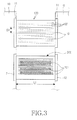
- FIG. 3 illustrates a connection structure between boards according to the present invention.
- a signal connector 11 and a power source connector 12 are mounted at the edge of each of a plurality of boards 10.
- the signal connectors 11 are connected by a signal cable 100 and the power source connectors 12 are connected by a power source cable 200.
- the signal cable 100 includes a plurality of signal lines 102 for transmitting various communication signals and signals for controlling various parts.
- the power source cable 200 includes a plurality of power source lines 201 for supplying power to various parts.
- signal connectors 11 and the power source connectors 12 are separately mounted and are connected by the signal cable 100 and the power source cable 200 independently of each other in an embodiment of the present invention, either the signal connectors 11 or the power source connectors 12 may be connected by a corresponding cable and signal lines and power source lines may be independently arranged within the cable.
- connection lines of the signal cable 100 and the power source cable 200 have small widths and thicknesses in accordance with the specification of the signal connector 11 and the power source connector 12, their inductance and AC resistance increase.
- the power source lines 201 having large inductance and AC resistance may not provide stable power to a device during a high-speed operation, or a large voltage drop may occur.
- a voltage drop V L caused by the inductance L is L(di/dt). Since a change di/dt in a supply current required for the high-speed operation is large, a voltage actually supplied to a device undergoes large fluctuation.
- a plurality of power source lines having a large di/dt in the power source cable 200 is arranged in parallel adjacent to one another and the remaining portions except for connector connection portions are connected.
- the remaining portions of the power source lines except for connector connection portions are connected to form a single plane conducting line, instead of simply connecting the power source lines in parallel.
- the number of power source lines to be connected is determined by an operation speed, an operating current used, and a power source characteristic. As an operation speed increases, an operating current increases. As a result, the number of required power source lines also increases.
- FIG. 3 five power source lines, three power source lines, and four power source lines of the power cable 200 are connected, respectively, thereby forming three plane conducting lines.
- inductance and resistance can be reduced, thereby achieving stable power supply during a high-speed operation.
- a ground connection should have low inductance to guarantee a stable operation.
- a lumped circuit condition cannot be satisfied.
- a ground cannot be implemented through one or two connections.
- a plurality of ground lines 101 is used and at least one ground line 101 is arranged at predetermined intervals D1, instead of simply connecting the ground lines 101 in parallel.
- the ground lines 101 are arranged at predetermined intervals D1 between the signal lines 102 in the signal cable 100, i.e., each ground line is arranged for every four signal lines 102.
- the ground lines 101 are not arranged successively, but are arranged at predetermined intervals.
- the interval D1 between the ground lines 101 is determined according to a maximum frequency operating in the boards 10.
- a length L1 of a cable between the boards 10 is determined according to the maximum frequency.
- the maximum frequency ranges from 800MHz to 2.1 GHz according to a supported band.
- the interval D1 and the length L1 are designed such that D1 ⁇ c1 (kf) and L1 ⁇ c2(kf). k is 20 if a conservative condition is applied and is 12 if a general condition is applied.
- the ground line 101 When the ground line 101 is arranged between the signal lines 102, at least one ground line 101 may be arranged and the interval D1 between the ground lines 101 is smaller than the calculated value.
- the interval D1 is not necessarily constant.
- ground lines 101 can also be applied to the power source cable 200 as well as the signal cable 100.
- the ground lines 101 when the ground lines 101 are arranged in the power source cable 200, at least one ground line 101 may be arranged between plane conducting lines.
Landscapes
- Engineering & Computer Science (AREA)
- Signal Processing (AREA)
- Microelectronics & Electronic Packaging (AREA)
- Computer Networks & Wireless Communication (AREA)
- Coupling Device And Connection With Printed Circuit (AREA)
- Telephone Set Structure (AREA)
- Combinations Of Printed Boards (AREA)
Applications Claiming Priority (1)
| Application Number | Priority Date | Filing Date | Title |
|---|---|---|---|
| KR1020050089049A KR100713445B1 (ko) | 2005-09-24 | 2005-09-24 | 다수개의 보드로 구성된 휴대 단말기의 보드간 연결 구조 |
Publications (2)
| Publication Number | Publication Date |
|---|---|
| EP1768472A2 true EP1768472A2 (de) | 2007-03-28 |
| EP1768472A3 EP1768472A3 (de) | 2008-06-25 |
Family
ID=37497957
Family Applications (1)
| Application Number | Title | Priority Date | Filing Date |
|---|---|---|---|
| EP06119552A Withdrawn EP1768472A3 (de) | 2005-09-24 | 2006-08-25 | Verbindungsstruktur zwischen einer Mehrzahl von Leiterplatten eines tragbaren Endgeräts |
Country Status (4)
| Country | Link |
|---|---|
| US (1) | US20070070609A1 (de) |
| EP (1) | EP1768472A3 (de) |
| KR (1) | KR100713445B1 (de) |
| CN (1) | CN100452544C (de) |
Families Citing this family (10)
| Publication number | Priority date | Publication date | Assignee | Title |
|---|---|---|---|---|
| JP4237160B2 (ja) * | 2005-04-08 | 2009-03-11 | エルピーダメモリ株式会社 | 積層型半導体装置 |
| JP4914797B2 (ja) * | 2007-10-05 | 2012-04-11 | 株式会社フジクラ | フレキシブル基板と端子金具との接続構造 |
| KR20090067744A (ko) | 2007-12-21 | 2009-06-25 | 엘지전자 주식회사 | 연성 필름 |
| KR100896439B1 (ko) * | 2007-12-26 | 2009-05-14 | 엘지전자 주식회사 | 연성 필름 |
| KR100939550B1 (ko) * | 2007-12-27 | 2010-01-29 | 엘지전자 주식회사 | 연성 필름 |
| KR100947607B1 (ko) * | 2007-12-27 | 2010-03-15 | 엘지전자 주식회사 | 연성 필름 |
| KR101054433B1 (ko) * | 2007-12-27 | 2011-08-04 | 엘지전자 주식회사 | 연성 필름 및 그를 포함하는 표시장치 |
| KR100889002B1 (ko) * | 2007-12-27 | 2009-03-19 | 엘지전자 주식회사 | 연성 필름 |
| KR100947608B1 (ko) * | 2007-12-28 | 2010-03-15 | 엘지전자 주식회사 | 연성 필름 |
| CN102122541B (zh) * | 2010-12-24 | 2013-03-27 | 领亚电子科技股份有限公司 | 一种特殊串行eSATA超高速数据传输线及制备该传输线的模具 |
Family Cites Families (14)
| Publication number | Priority date | Publication date | Assignee | Title |
|---|---|---|---|---|
| US4679868A (en) * | 1985-08-27 | 1987-07-14 | E. I. Du Pont De Nemours And Company | Multiconductor electrical cable terminations and methods and apparatus for making same |
| JPH034464A (ja) * | 1989-05-30 | 1991-01-10 | Riyousei Denso Kk | フラットケーブルコネクタ |
| CN2078930U (zh) * | 1990-09-06 | 1991-06-12 | 上海市东海军工技术工程公司 | 室内型全频道电视平面放大天线 |
| JPH0787728A (ja) * | 1993-09-20 | 1995-03-31 | Ricoh Co Ltd | 電子機器 |
| US5539360A (en) * | 1994-03-11 | 1996-07-23 | Motorola, Inc. | Differential transmission line including a conductor having breaks therein |
| JPH0837351A (ja) * | 1994-07-21 | 1996-02-06 | Amp Japan Ltd | フレキシブル回路板ハーネス装置及びそれに使用されるフレキシブル回路板 |
| JP2891665B2 (ja) * | 1996-03-22 | 1999-05-17 | 株式会社日立製作所 | 半導体集積回路装置およびその製造方法 |
| KR100238289B1 (ko) * | 1997-06-16 | 2000-01-15 | 윤종용 | 테이프 레코더의 카세트 홀더 결합 구조체 |
| FR2841394B1 (fr) * | 2002-06-24 | 2004-11-19 | Framatome Connectors Int | Dispositif de connexion pour circuit souple |
| CN2618321Y (zh) * | 2003-03-12 | 2004-05-26 | 富士康(昆山)电脑接插件有限公司 | 电连接器端子 |
| US7531752B2 (en) * | 2003-07-24 | 2009-05-12 | Nec Corporation | Flexible substrate and electronic device |
| US7158817B2 (en) * | 2005-03-17 | 2007-01-02 | Masaharu Kubo | Portable terminal |
| KR20080054951A (ko) * | 2006-12-14 | 2008-06-19 | 삼성전자주식회사 | 휴대용 단말기 |
| KR100850209B1 (ko) * | 2007-02-08 | 2008-08-04 | 삼성전자주식회사 | 전력을 효율적으로 관리할 수 있는 시스템 인 패키지반도체 장치 및 그에 따른 전력 관리 방법 |
-
2005
- 2005-09-24 KR KR1020050089049A patent/KR100713445B1/ko not_active Expired - Fee Related
-
2006
- 2006-05-17 CN CNB2006100825546A patent/CN100452544C/zh not_active Expired - Fee Related
- 2006-08-25 EP EP06119552A patent/EP1768472A3/de not_active Withdrawn
- 2006-09-25 US US11/526,435 patent/US20070070609A1/en not_active Abandoned
Also Published As
| Publication number | Publication date |
|---|---|
| US20070070609A1 (en) | 2007-03-29 |
| KR20070034402A (ko) | 2007-03-28 |
| KR100713445B1 (ko) | 2007-04-30 |
| EP1768472A3 (de) | 2008-06-25 |
| CN100452544C (zh) | 2009-01-14 |
| CN1937321A (zh) | 2007-03-28 |
Similar Documents
| Publication | Publication Date | Title |
|---|---|---|
| EP2280591B1 (de) | Mobiles Endgerät mit flexibler Leiterplatte | |
| DE19919383A1 (de) | Antenne vom Oberflächenbefestigungstyp, Antennenvorrichtung und Kommunikationsvorrichtung mit der Antennenvorrichtung | |
| EP1601045A3 (de) | Die Abschirmung als zweite Antenne verwendendes tragbares und klappbares Telefon | |
| CN102005640A (zh) | 无线通信装置 | |
| EP1415270B1 (de) | Datenträger mit einer kontaktenmatrix | |
| EP1328068A1 (de) | Erdungseinrichtung für tragbares Radioendgerät | |
| TWI267092B (en) | Anisotropic conductive sheet | |
| DE60308903T2 (de) | Auf einer oberfläche montierbare klemme zur verwendung für ein mobiles kommunikationsgerät | |
| US20070070609A1 (en) | Connection structure between plurality of boards of portable terminal | |
| US5999831A (en) | Portable radio | |
| JP2002158420A (ja) | プリント基板の電源線および信号線の接続方法ならびに電気機器 | |
| KR20210120888A (ko) | 전면 및 후면 안테나를 갖는 무선 주파수 배치 | |
| EP0707355B1 (de) | Antenne | |
| CN105552498B (zh) | 可挠式传输装置及通信装置 | |
| US20070212938A1 (en) | Connection cable between printed circuit boards of a portable terminal | |
| US8072390B2 (en) | Antenna arrangement | |
| US8106831B2 (en) | Circuit board and telephone apparatus | |
| EP1229618B1 (de) | Entladungsspaltvorrichtung | |
| EP0707354A1 (de) | Antenne | |
| US7542260B2 (en) | Motherboard | |
| CN216436134U (zh) | 天线结构和蓝牙通讯装置 | |
| EP1732161A1 (de) | Interne Antenne und mobiles Kommunikationsgerät mit solch einer Antenne | |
| Kim et al. | A Low EMI Board-to-board Connector Design for 5G mmWave and High-speed Signaling | |
| US20180034132A1 (en) | Electronic device | |
| US6542382B2 (en) | Densely arranged electrically shielded communication panels |
Legal Events
| Date | Code | Title | Description |
|---|---|---|---|
| PUAI | Public reference made under article 153(3) epc to a published international application that has entered the european phase |
Free format text: ORIGINAL CODE: 0009012 |
|
| 17P | Request for examination filed |
Effective date: 20060825 |
|
| AK | Designated contracting states |
Kind code of ref document: A2 Designated state(s): AT BE BG CH CY CZ DE DK EE ES FI FR GB GR HU IE IS IT LI LT LU LV MC NL PL PT RO SE SI SK TR |
|
| AX | Request for extension of the european patent |
Extension state: AL BA HR MK YU |
|
| PUAL | Search report despatched |
Free format text: ORIGINAL CODE: 0009013 |
|
| RIC1 | Information provided on ipc code assigned before grant |
Ipc: H01B 7/08 20060101ALI20080428BHEP Ipc: H05K 1/14 20060101AFI20061215BHEP |
|
| AK | Designated contracting states |
Kind code of ref document: A3 Designated state(s): AT BE BG CH CY CZ DE DK EE ES FI FR GB GR HU IE IS IT LI LT LU LV MC NL PL PT RO SE SI SK TR |
|
| AX | Request for extension of the european patent |
Extension state: AL BA HR MK RS |
|
| 17Q | First examination report despatched |
Effective date: 20080908 |
|
| AKX | Designation fees paid |
Designated state(s): DE FR GB |
|
| STAA | Information on the status of an ep patent application or granted ep patent |
Free format text: STATUS: THE APPLICATION IS DEEMED TO BE WITHDRAWN |
|
| 18D | Application deemed to be withdrawn |
Effective date: 20090120 |