EP1770851A2 - Verfahren zur Vorhersage der Junktionstemperatur und Vorrichtung zur Verwendung in einem Leistungswandlermodul - Google Patents
Verfahren zur Vorhersage der Junktionstemperatur und Vorrichtung zur Verwendung in einem Leistungswandlermodul Download PDFInfo
- Publication number
- EP1770851A2 EP1770851A2 EP06019883A EP06019883A EP1770851A2 EP 1770851 A2 EP1770851 A2 EP 1770851A2 EP 06019883 A EP06019883 A EP 06019883A EP 06019883 A EP06019883 A EP 06019883A EP 1770851 A2 EP1770851 A2 EP 1770851A2
- Authority
- EP
- European Patent Office
- Prior art keywords
- devices
- temperature
- thermal impedance
- switching device
- switching
- Prior art date
- Legal status (The legal status is an assumption and is not a legal conclusion. Google has not performed a legal analysis and makes no representation as to the accuracy of the status listed.)
- Granted
Links
Images


Classifications
-
- H—ELECTRICITY
- H02—GENERATION; CONVERSION OR DISTRIBUTION OF ELECTRIC POWER
- H02M—APPARATUS FOR CONVERSION BETWEEN AC AND AC, BETWEEN AC AND DC, OR BETWEEN DC AND DC, AND FOR USE WITH MAINS OR SIMILAR POWER SUPPLY SYSTEMS; CONVERSION OF DC OR AC INPUT POWER INTO SURGE OUTPUT POWER; CONTROL OR REGULATION THEREOF
- H02M7/00—Conversion of AC power input into DC power output; Conversion of DC power input into AC power output
-
- G—PHYSICS
- G01—MEASURING; TESTING
- G01K—MEASURING TEMPERATURE; MEASURING QUANTITY OF HEAT; THERMALLY-SENSITIVE ELEMENTS NOT OTHERWISE PROVIDED FOR
- G01K7/00—Measuring temperature based on the use of electric or magnetic elements directly sensitive to heat ; Power supply therefor, e.g. using thermoelectric elements
- G01K7/42—Circuits effecting compensation of thermal inertia; Circuits for predicting the stationary value of a temperature
- G01K7/425—Thermal management of integrated systems
-
- H—ELECTRICITY
- H02—GENERATION; CONVERSION OR DISTRIBUTION OF ELECTRIC POWER
- H02M—APPARATUS FOR CONVERSION BETWEEN AC AND AC, BETWEEN AC AND DC, OR BETWEEN DC AND DC, AND FOR USE WITH MAINS OR SIMILAR POWER SUPPLY SYSTEMS; CONVERSION OF DC OR AC INPUT POWER INTO SURGE OUTPUT POWER; CONTROL OR REGULATION THEREOF
- H02M1/00—Details of apparatus for conversion
- H02M1/32—Means for protecting converters other than automatic disconnection
Definitions
- the present invention relates to integrated gate bipolar transistor (IGBT) modules and more specifically to a method and apparatus for predicting the junction temperatures of IGBTs in an IGBT module operating at a low frequency or a DC condition.
- IGBT integrated gate bipolar transistor
- IGBTs are used in many different types of power conditioning modules including AC to DC converters, DC to AC inverters, AC-DC-AC converters, etc.
- DC-AC inverter six IGBTs are arranged to form an inverter bridge along with six diodes.
- IGBTs and diodes During switching operations IGBTs and diodes generate heat that has a magnitude related to the switching frequency as well as the amount of current passing through the devices. When IGBT or diode junction temperature exceeds a specific threshold temperature associated with a device type, the devices have been known to fail. In order to reduce failure rate, IGBTs and diodes used in power conditioning modules are typically mounted to heat dissipating devices such as air or liquid cooled heat sinks and are rated for specific current levels/switching frequencies.
- NTC sensor negative temperature coefficient sensor
- switching devices e.g., IGBTs, diodes
- switching devices e.g., IGBTs, diodes
- a substantial distance e.g., three device width dimensions
- a single heat sink having a single mounting surface is provided where all of the IGBTs and diodes that comprise a conditioning circuit are mounted to the single mounting surface.
- the conventional prediction method described above has been shown to be inaccurate.
- heat form one device tends to heat up adjacent devices.
- heat from one device tends to increase the temperature of adjacent devices under all operating conditions, the neighbor heating effect is exacerbated at low switching frequencies and when a conditioning circuit is operated under DC conditions. For instance, in at least some experiments it has been observed that under DC conditions in a six-pack IGBT inverter module, a maximum prediction error of nearly 30 degrees Celsius has occurred when using th conventional prediction method.
- the accuracy of a junction temperature prediction algorithm can be increased substantially by accounting for the effects of at least some inter-module switching device heating as well as the effects of other ambient heating characteristics.
- the present invention includes methods and apparatus that relatively accurately predict switching device junction temperature by accounting for at least a subset of heating characteristics of adjacent devices and at least a subset of module impedances.
- At least some inventive embodiments include a method for predicting junction device temperature of at least a first switching device in a power conversion module that includes the first switching device and at least a second switching device, the method comprising the steps of identifying a cross thermal impedance value indicative of how the temperature of the second switching device effects the first switching device temperature and using the cross thermal impedance value to predict the temperature of the at least a first switching device.
- the module includes, in addition to the first and second devices, a plurality of additional switching devices and wherein the method further includes the steps of identifying a cross thermal impedance for each of the plurality of additional devices indicative of how the temperature of the additional device effects the first switching device temperature and using all of the cross thermal impedance values to predict the temperature of the at least a first switching device.
- the cross thermal impedance between the second and first devices is a first impedance value and the module includes, in addition to the first and second devices, at least a third switching device and wherein the method further includes the steps of identifying a second cross thermal impedance that is indicative of how the temperature of the third device effects the first device temperature where the first and second cross thermal impedance values are different.
- the method further includes the step of identifying a self thermal impedance value associated with the first switching device, the step of using the cross thermal impedance including mathematically combining the self thermal impedance and the cross coupling impedance to predict the first switching device temperature.
- the method further includes the steps of providing a temperature sensor at least proximate the module, identifying at least one coupling thermal impedance from the second switching device to the sensor and generating a temperature value via the sensor, the step of using the cross thermal impedance including the step of mathematically combining the cross coupling impedance, the at least one coupling thermal impedance to the sensor, the temperature value generated by the sensor and the self impedance of the first switching device to predict junction temperature of the first switching device.
- each of the switching devices are one of a diode and an IGBT.
- Some embodiments include a method for predicting junction device temperature of at least a first switching device in a power conversion module that includes a plurality of switching devices, the method comprising the steps of during switching activity, identifying at least one operating characteristic of the first switching device and solving an equation that uses the identified operating characteristic to predict the temperature of the first switching device where the equation solved is a function of the location of the first switching device with respect to the other switching devices in the plurality.
- the operating characteristic is the power loss of the first switching device.
- the equation accounts for power losses of switching devices adjacent the first switching device as well as cross thermal impedance between the adjacent devices and the first switching device and wherein the method further includes the steps of identifying a cross thermal impedance between a switching device adjacent the first switching device and the first switching device and, during switching activity, identifying the power losses of switching devices adjacent the first switching device.
- the switching devices adjacent the first switching device are neighboring devices and wherein the equation accounts for power losses of switching devices adjacent the neighboring devices as well as cross thermal impedance between the devices adjacent the neighboring devices and wherein the method further includes the steps of identifying a cross thermal impedance between a switching device adjacent a neighboring switching device and the first switching device and, during switching activity, identifying the power losses of switching devices adjacent the first switching device.
- Some embodiments include a method for predicting junction device temperatures of at least a subset of devices in a power conversion module that includes a heat sink that forms a mounting surface, six IGBT devices and six diode devices that are mounted to the mounting surface, the method comprising the steps of identifying cross thermal impedance values indicative of the effect that temperature of adjacent devices have on each other, during switching activity, identifying power losses of at least a subset of the devices and using the device power loss values and the cross thermal impedance values to predict the temperatures of at least a subset of the module devices.
- the step of identifying power losses includes identifying power losses of each of the module devices and wherein the step of using the power loss values and the cross thermal impedance values includes using the values to predict the temperatures of each of the module devices.
- the method further includes the steps of providing a temperature sensor at least proximate the module and sensing the temperature of the module via the sensor, the step of using the values to predict the temperatures of at least a subset of the module devices including also using the sensed temperature value.
- the method further includes the step of identifying thermal coupling impedances between the sensor and at least a subset of the devices, the step of using the values to predict the temperatures of at least a subset of the module devices also including using the thermal coupling impedances.
- the method further includes the step of identifying a self impedance value for each of the module devices and, during switching activity, identifying power losses for each of the devices, the step of using the values to predict the temperatures also including using the self impedance values and the power losses of each of the devices.
- some embodiments include an apparatus for use with a module that includes a plurality of electronic switching devices, the apparatus for predicting the junction temperature of at least a first of the switching devices, the apparatus comprising a processor that runs a program to perform the steps of identifying power loss of at least a second of the switching devices using the power loss value of the at least a second switching device to predict the temperature of the first switching device junction.
- the apparatus further includes a database in which is stored a cross thermal impedance value indicative of the thermal impedance between the first and second devices, the processor using the power loss value and the cross thermal impedance to predict the temperature of the first switching device junction.
- the database includes cross thermal impedance values for a sub-set of the devices in addition to the second device that are indicative of the thermal impedance between each of the other devices and the first device, the processor further identifying power loss values for each of the sub-set of devices and using all of the power loss values and the cross thermal impedance values to predict the temperature of the first switching device junction.
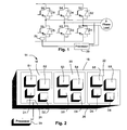
- Fig. 1 is a schematic view of a three phase inverter
- Fig. 2 is a perspective view of inverter IGBTs and diodes mounted to a mechanical heat sink;
- Fig. 3 is a schematic diagram illustrating an equivalent circuit of the thermal impedance between a device junction and a case layer for which manufacturers typically provide values;
- Fig. 4 is a schematic diagram similar to Fig. 3, albeit illustrating an equivalent circuit that includes additional components that account for self-impedance of devices;
- Fig. 5 is similar to Fig. 3, albeit illustrating an equivalent circuit representing coupling thermal impedance from a neighbor device;
- Fig. 6 is similar to Fig. 3, albeit illustrating an equivalent circuit representing coupling thermal impedance from an inverter device to a NTC temperature sensor;
- Fig. 7 is a graph illustrating experimental and curve fitted device temperatures for diode D3 in Fig. 2 when diode D3 is powered;
- Fig. 8 is similar to Fig. 7, albeit illustrating curves corresponding to switch S4 in Fig. 2 when diode D4 is powered;
- Fig. 9 is similar to Fig. 7, albeit illustrating curves corresponding to switch S3 when switch S4 is powered.
- Module 10 includes six IGBT switch devices S1-S6 and six diodes (also generally referred to as switching devices) D1-D6, a separate diode linked to each of the IGBTs in inverse parallel relationship.
- the IGBT switches are linked in series pairs across positive and negative DC buses and a central node of each pair is linked to a separate phase of a three phase load 12 (e.g., motor).
- a three phase load 12 e.g., motor
- current sensors 23 are linked to the motor supply lines for, as the label implies, sensing line currents.
- An NTC temperature sensor 24 is mounted proximate at least one of the switching devices for measuring a temperature proximate the devices.
- a processor 29 receives signals from the current sensor and NTC sensor 24 and uses the received signals to predict temperatures of the inverter devices.
- a perspective view of a six-pack inverter module 14 which includes a mechanical heat sink 16, three mounting substrates 18, 20 and 22, IGBTs S1-S6, diodes D1-D6 and the NTC temperature sensor 24.
- the sink includes a flat mounting surface 26.
- IGBT pairs and associated diodes are each mounted via a separate one of the substrates to the mounting surface 26.
- IGBTs S1 and S2 and associated diodes D1 and D2 are mounted to surface 26 with substrate 18 between the devices S1, S2, D1 and D2 and the sink mounting surface 26, devices S3, S4, D3 and D4 are mounted to surface 26 with substrate 20 between the devices and surface 26, and so on.
- substrates 18, 20 and 22 are arranged in a single row so that substrate 20 is between substrates 18 and 22.
- NTC sensor 24 is located inside a corner of module 14.
- one or more fan modules may be provided adjacent the rear sink surface that forms fins to facilitate sink cooling activity.
- the thermal impedance between a device junction and a device case for each IGBT or diode can be physically represented by four parallel RC sub-circuits which, unless indicated otherwise, will be referred to as "layers" hereinafter.
- the four layers can be arranged in series as illustrated in Fig. 3 to transform the physical representation to a mathematical representation. Note that after the transformation as shown in Fig. 3, the "layers" of the sub-circuit become meaningless.
- the thermal resistance and time constant values corresponding to the R and C components are typically provided by device manufacturers. Exemplary thermal resistances and time constants for each of the four layers are shown in table 1 that correspond to a EUPEC FS150R12KE3 power conversion module.
- ZI jc R i ⁇ 1 / / C i ⁇ 1 + R i ⁇ 2 / / C i ⁇ 2 + R i ⁇ 3 / / C i ⁇ 3 + R i ⁇ 4 / / C i ⁇ 4
- ZD jc R d ⁇ 1 / / C d ⁇ 1 + R d ⁇ 2 / / C d ⁇ 2 + R d ⁇ 3 / / C d ⁇ 3 + R d ⁇ 4 / / C d ⁇ 4
- ZI jc and ZD jc are the junction to case thermal impedance of an IGBT device and a diode device respectively
- R ik and C ik are the thermal resistance and capacitance of the k th layer of each IGBT device, respectively
- a sink layer RC sub-circuit including R L5 and C L5 represents a temperature increase in thermal grease associated with the device to sink interface planes and the aluminum of the heat sink.
- An ambient layer RC sub-circuit including R L6 and C L6 represents the temperature increase between the interface plane of the heat sink and the plane of the ambient (i.e., between the sink and the air beneath the sink.
- the IGBT and diode devices in a power conversion module are mounted to the sink in very close proximity to each other and therefore thermal coupling between devices must be considered to accurately predict device temperature.
- the coupling thermal impedance between IGBT and diode devices on a sink can be physically approximated by two additional layers represented by parallel RC sub-circuits.
- One is the sink layer which represents the temperature increase from case to sink across the thermal grease and from grease to ambient across the heat sink.
- the other is the ambient layer that represents the temperature increase of the air beneath the heat sink.
- the coupling thermal impedance between an IGBT or diode device and a neighboring device can be mathematically represented as illustrated in Fig.
- ZII ij ZII 5 ⁇ ij + ZII 6 ⁇ ij
- ZID ij ZID 5 ⁇ ij + ZID 6 ⁇ ij
- ZII 5ij and ZID 5ij are the coupling thermal impedances from the i th IGBT to the j th IGBT and the j th diodes at the sink layer, respectively
- ZII 6ij and ZID 6ij are the coupling thermal impedances from the i th IGBT to the j th IGBT and the j th diodes at the ambient layer
- ZDD ij ZID 5 ⁇ ij + ZID 6 ⁇ ij
- ZDI ij and ZDD ij are the coupling thermal impedances from the i th diode to the j th IGBT and j th diode, respectively
- ZDI5 ij and ZDD5 ij are the coupling thermal impedances from the i th diode to the j th IGBT and j th diodes at the sink layer, respectively
- ZDI6 ij and ZDD6 ij are the coupling thermal impedances from the i th IGBT to the j th IGBT and the j th diodes at the ambient layer, respectively.
- the total temperature increase of one device between its junction to ambient that is attributable to the other devices is the sum of the contributions from all module IGBTs and diodes as shown in the following equations:
- TI k is the junction temperature of the k th IGBT
- TD k is the junction temperature of the k th diode
- PI k is the power loss of the k th IGBT
- PD k is the power loss of the k th diode
- T amb is the ambient temperature.
- the IGBT and diode temperatures are generally predicted using a temperature value identified by the NTC sensor 24 (see Fig. 2).
- the NTC sensor is separated from the device junctions and thus thermal impedance exists between the junctions and the NTC sensor such that the sensor generated value does not accurately reflect the junction temperature. For this reason, the influence of the thermal impedance between the device junctions and the NTC sensor should be accounted to accurately predict junction temperature.
- the NTC temperature can be predicted by knowing device losses and the distance of the devices to the NTC sensor.
- a two layer RC circuit that represents the coupling thermal impedance from the IGBT and diode devices mounted on a sink to the NTC sensor is shown in Fig.
- T ntc The total temperature increase T ntc of an NTC can be expressed as.
- ZII, ZDI, ZID, and ZDD are each 6x6 matrices that represent the coupling thermal impedance matrix from the IGBTs to the IGBTs, from the IGBTs to the diodes, from the diodes to IGBTs and from the diodes to the diodes, respectively.
- ZID ZID 11 ZID 12 ⁇ ZID 16 ZID 21 ZID 22 ⁇ ZID 26 ⁇ ⁇ ⁇ ⁇ ZID 61 ZID 62 ⁇ ZID 66
- ZDD [ ZDD 11 ZDD 12 ⁇ ZDD 16 ZDD 21 ZDD 22 ⁇ ZDD 26 ⁇ ⁇ ⁇ ⁇ ZDD 61 ZDD 62 ⁇ ZDD 66 ] where ZII ij , ZDI ij , ZID ij
- Equations 14 and 15 are relatively complex and would be somewhat burdensome to solve using a standard drive microprocessor. For this reason, hereafter, several assumptions are made that enable simplification of Equations 14 and 15. To this end, based on the locations of the IGBTs and diodes as shown in Fig. 2, several assumptions and approximations can be made to simplify the equations.
- the coupling impedances associated with neighboring or adjacent devices that are an identical or similar distance away from one device should be approximately equal or at least similar enough that the differences between these coupling impedances are trivial and can be neglected such that: ZII 5 ⁇ ij ⁇
- the coupling impedances between devices that are separated by relatively large distances can be neglected. For example, while adjacent devices and devices that are one or two device dimensions (i.e., one or two device widths) away from a first device may effect the temperature of the first device, devices that are three or more device dimensions away from the first device will only have a negligible effect on the temperature of the first device and thus the effect can be ignored without significantly effecting the final temperature prediction.
- > 2 ZDI 5 ⁇ ij
- > 2 ZID 5 ⁇ ij ⁇
- > 2 ZDD 5 ⁇ ij ⁇
- > 2 0
- i > 2 ZDN 5 ⁇ i ⁇
- i > 2 0
- IGBT temperature vector equation ZI 0 + Z jc ⁇ I 6 + Z ⁇ PI + ZDI 0 ⁇ I 6 + Z ⁇ PD + P ⁇ Zamb ⁇ A + Tamb
- Equations 20 and 22 can be combined to yield the following equation for predicting the IGBT junction temperatures from the NTC sensor temperature value and power losses:
- equations 20 and 21 can be combined to yield the following equation for predicting the diode junction temperatures from the NTC sensor temperature value and the power losses:
- Equations 23 and 24 the ambient layer impedance and the ambient temperature from Equations 21 and 22 both cancel when Equations 23 and 24 are formulated.
- the thermal impedances in Equation 23 and 24 can be directly calculated by applying pulsed current through each IGBT and each diode device on the module.
- each IGBT and diode device may be injected with a 100A, 250 second current pulse and the temperature of the device during the pulse can be directly measured and recorded.
- the corresponding thermal impedances can then be calculated by a curve fitting program (e.g., a program built up using Matlab which is owned by MathWorks, Inc., or some similar type of software).
- Fig. 7 shows the experimental result of the real temperature and the curve fitted temperature of third diode D3 when the third diode is powered.
- Fig. 8 shows the experimental result of the real temperature and the curve fitted temperature of fourth IGBT S4 when the fourth diode D4 is powered. In Fig. 8 it can be seen that the temperature of diode D4 clearly effects the temperature of adjacent IGBT S4.
- Fig. 9 shows the experimental result of the real temperature and the curve fitted temperature of third IGBT S3 when the fourth IGBT S4 is powered. In Fig. 9 it can be seen that the temperature of IGBT S4 clearly effects the temperature of adjacent IGBT S3.
- Exemplary coupling impedance values determined using the curve fitting software and Equations 23 and 24 are listed in tables 2, 3 and 4 with the thermal impedance values of the sink layer shown in Table 2, the coupling thermal impedance of the ambient layer shown in Table 3 and the coupling thermal impedance values from the IGBTs and diodes to the NTC sensor shown in table 4.
- Equations 25 and 26 Comparing the values expressed in Equations 25 and 26 to the coupling thermal impedance values (e.g., Z 1 , Z 2 , Z 3 , etc.) shown in tables 2 and 3, the following conclusions can be made.
- the coupling thermal impedances Z 1 , Z 2 between neighbor chips are much smaller than the self impedance and therefore impedance values Z 1 , Z 2 can have at least some error without significantly effecting temperature prediction accuracy.
- the coupling thermal impedance in the ambient layer see Table 3 is trivial when compared to the self impedance and therefore a uniform thermal impedance can be assumed without significantly effecting temperature prediction accuracy.
- the temperature prediction Equations 23 and 24 have been used to predict the junction temperatures of module devices where the devices have been operated under DC conditions. During testing, four models were investigated and compared with each other so that the accuracy of Equations 23 and 24 could be ascertained.
- the first model is called "R jc model" in which a uniform case temperature was assumed.
- the NTC temperature is assumed to be equal to the case layer.
- the second model is referred to as the "No neighbor" model because, as the label implies, the model did not account for the thermal coupling between neighboring or adjacent IGBTs and diodes.
- Z 1 and Z 2 each were equal to zero in the temperature prediction equations above (i.e., in equations 23 and 24 and the Z matrix as shown in Equation 20).
- the thermal impedances of the devices themselves e.g., ZII 0 , ZDD 0 ) were considered.
- the third model is referred to as the "one neighbor" model because the model includes equations that consider the coupling thermal impedance between the devices that are closest or immediately adjacent a specific device for which the junction temperature is being predicted.
- the coupling thermal impedance is neglected when a device is separated from a device for which the temperature is being predicted by at least one other device.
- Z 2 was set equal to zero in Equations 20, 23 and 24.
- the fourth model is referred to as the "two neighbor" model because the model includes equations that consider the coupling thermal impedance between devices immediately adjacent a device for which temperature is being predicted as well as devices that are adjacent the immediately adjacent devices (i.e., devices that are no more than two devices away from the device for which temperature is being predicted.
- the coupling thermal impedance is neglected when a device is separated from a device for which the temperature is being predicted by at least two other device.
- an inverter module akin to module 14 illustrated in Fig. 2 was operated under the following conditions: DC bus voltage: 300V Switching frequency: 2kHz ⁇ 10kHz Load current amplitude: 20A ⁇ 100A Load current angle: 0° ⁇ 330° Ambient temperature: 22°C
- the maximum temperature increase of the hottest device during testing was approximately 110°C.
- Table 5 shows the maximum and minimum temperature prediction errors Max(T err ) and Min(T err ), respectively, for all IGBTs and diodes for each of the four models.
- Terr is defined as the predicted junction minus the tested temperature and is positive when the predicted temperature is higher than the tested result.
- the voltage drops of the IGBTs and diodes were calculated in detail by considering the influence of the junction temperature. The resulting temperature errors are shown in Table 5.
- the maximum voltage drops were also calculated using a worst case 125° Celsius V/I curve and neglecting the junction temperature influence on the voltage drops.
- the "one neighbor model” is the simplest model that yields relatively accurate results and that the "two neighbor model” is not significantly more accurate than the one neighbor model.
- Equations 23 and 24 after values required to solve Equations 23 and 24 have been determined via Mathlab or some other similar product, the values can be used in Equations 23 and 24 during normal operation of the associated module 14 (see again Fig. 2) to predict device temperatures.
- thermal model has been developed for a six-pack insulated gate bipolar transistor (IGBT) power module operating as a three phase voltage source inverter. With this method, two more thermal layers are added to the system to predict the chip temperatures from the NTC sensor value.
- the inventive model increases the temperature prediction accuracy when the inverter operates at zero or low output frequency.
- the model is not complicated and can be easily integrated into a micro-controller programs for dynamic temperature prediction.
- module that includes IGBTs
- the invention is applicable to other modules that include other device types such as, for instance, MOSFETs, IGCTs, etc.
- the NTC is described above as being located on the module case, in at least some embodiments the NTC may be located elsewhere and still very close to the module and satisfactory results will still occur.
- circuits illustrated in Figs. 3-6 do not represent exact system impedances but rather are predictive in nature.
- equations based on Figs. 3-6 and modified above based on various assumptions are not precise and instead are predictive in nature.
- the invention discloses a method and apparatus for predicting junction device temperature of at least a first switching device in a power conversion module that includes the first switching device and at least a second switching device, the method comprising the steps of identifying a cross thermal impedance value indicative of how the temperature of the second switching device effects the first switching device temperature an using the cross thermal impedance value to predict the temperature of the at least a first switching device.
Landscapes
- Engineering & Computer Science (AREA)
- Power Engineering (AREA)
- Physics & Mathematics (AREA)
- General Physics & Mathematics (AREA)
- Power Conversion In General (AREA)
- Inverter Devices (AREA)
Applications Claiming Priority (1)
| Application Number | Priority Date | Filing Date | Title |
|---|---|---|---|
| US11/238,005 US7356441B2 (en) | 2005-09-28 | 2005-09-28 | Junction temperature prediction method and apparatus for use in a power conversion module |
Publications (3)
| Publication Number | Publication Date |
|---|---|
| EP1770851A2 true EP1770851A2 (de) | 2007-04-04 |
| EP1770851A3 EP1770851A3 (de) | 2009-07-01 |
| EP1770851B1 EP1770851B1 (de) | 2014-07-02 |
Family
ID=37507324
Family Applications (1)
| Application Number | Title | Priority Date | Filing Date |
|---|---|---|---|
| EP06019883.5A Ceased EP1770851B1 (de) | 2005-09-28 | 2006-09-22 | Verfahren zur Vorhersage der Junktionstemperatur und Vorrichtung zur Verwendung in einem Leistungswandlermodul |
Country Status (3)
| Country | Link |
|---|---|
| US (3) | US7356441B2 (de) |
| EP (1) | EP1770851B1 (de) |
| CN (1) | CN1952631B (de) |
Cited By (6)
| Publication number | Priority date | Publication date | Assignee | Title |
|---|---|---|---|---|
| WO2009087150A1 (de) * | 2008-01-07 | 2009-07-16 | Woodward Seg Gmbh & Co. Kg | Verfahren zum betreiben einer windenergieanlage |
| CN101587507B (zh) * | 2009-06-25 | 2012-09-05 | 中国电力科学研究院 | 一种高压大功率晶闸管电热模型的建立方法 |
| EP2031753A3 (de) * | 2007-08-28 | 2014-02-26 | Rockwell Automation Technologies, Inc. | Reduzierung der Sperrschichttemperatur eines Leistungshalbleitermoduls in einem Dreiphasenwechselrichter |
| EP2325992A4 (de) * | 2008-09-11 | 2017-04-19 | Kabushiki Kaisha Yaskawa Denki | Umrichtervorrichtung, umrichtersteuerungssystem, motorsteuerungssystem und verfahren zur steuerung der umrichtervorrichtung |
| WO2020025220A1 (de) * | 2018-08-02 | 2020-02-06 | Volkswagen Aktiengesellschaft | Verfahren und vorrichtung zum schätzen der temperatur eines halbleiterbauelementes sowie computerprogramm |
| WO2022248059A1 (en) * | 2021-05-28 | 2022-12-01 | HELLA GmbH & Co. KGaA | Method for real-time estimation of temperatures of electric components in a power electronics system |
Families Citing this family (75)
| Publication number | Priority date | Publication date | Assignee | Title |
|---|---|---|---|---|
| JPS5933676B2 (ja) * | 1981-12-14 | 1984-08-17 | 旭化成株式会社 | メツキ用治具の被覆用樹脂組成物 |
| FR2915034B1 (fr) * | 2007-04-12 | 2009-06-05 | Schneider Toshiba Inverter | Methode et systeme de gestion de la temperature dans un variateur de vitesse |
| KR101364204B1 (ko) * | 2007-05-29 | 2014-02-17 | 엘지전자 주식회사 | 모터 드라이버 시스템 및 모터 드라이버 보호방법 |
| US7940034B2 (en) * | 2008-05-19 | 2011-05-10 | Infineon Technologies Austria Ag | Apparatus for detecting a state of operation of a power semiconductor device |
| US8054660B2 (en) * | 2008-05-19 | 2011-11-08 | GM Global Technology Operations LLC | Inverter module with thermally separated semiconductor devices |
| US7756669B2 (en) * | 2008-06-18 | 2010-07-13 | Gm Global Technology Operations, Inc. | Systems and methods for estimating temperatures of power module components |
| US7738267B1 (en) * | 2009-01-07 | 2010-06-15 | Rockwell Automation Technologies, Inc. | Systems and methods for common-mode voltage reduction in AC drives |
| US8380451B2 (en) * | 2009-07-14 | 2013-02-19 | Ford Global Technologies, Llc | System and method for monitoring the state of health of a power electronic system |
| US7881081B1 (en) | 2010-04-16 | 2011-02-01 | Rockwell Automation Technologies, Inc. | Systems and methods for reducing AC drive common-mode currents |
| US8471516B2 (en) * | 2010-05-24 | 2013-06-25 | Rockwell Automation Technologies, Inc. | Adjustable speed drive lifetime improvement method |
| US8223511B2 (en) | 2010-06-07 | 2012-07-17 | Rockwell Automation Technologies, Inc. | Common mode voltage reduction apparatus and method for current source converter based drive |
| US8488345B2 (en) | 2010-12-01 | 2013-07-16 | Rockwell Automation Technologies, Inc. | Pulse width modulation control method and system for mitigating reflected wave effects in over-modulation region |
| US9362839B2 (en) | 2011-02-09 | 2016-06-07 | Rockwell Automation Technologies, Inc. | Power converter with common mode voltage reduction |
| CN102636291B (zh) * | 2011-02-15 | 2013-12-25 | 三一电气有限责任公司 | 一种igbt结温检测装置及其方法 |
| US20120221288A1 (en) * | 2011-02-28 | 2012-08-30 | General Electric Company, A New York Corporation | System and Methods for Improving Power Handling of an Electronic Device |
| US8674651B2 (en) * | 2011-02-28 | 2014-03-18 | General Electric Company | System and methods for improving power handling of an electronic device |
| US8793314B2 (en) | 2011-05-20 | 2014-07-29 | BlendAbout, Inc. | Method and system for creating events and matching users via blended profiles |
| EP2541220B1 (de) * | 2011-06-28 | 2015-04-08 | Fraunhofer-Gesellschaft zur Förderung der angewandten Forschung e.V. | Vorrichtung zur Messung einer Temperatur eines Leistungshalbleiters |
| US8549462B2 (en) | 2011-08-23 | 2013-10-01 | International Business Machines Corporation | Thermal coupling determination and representation |
| KR101942027B1 (ko) * | 2012-03-28 | 2019-04-11 | 삼성전자 주식회사 | 디바이스의 온도 예측 방법 |
| JP5850251B2 (ja) * | 2012-05-21 | 2016-02-03 | 株式会社デンソー | 温度センサの異常判別装置および異常判別方法、電力変換装置 |
| JP5963860B2 (ja) * | 2012-06-14 | 2016-08-03 | 三菱電機株式会社 | パワーモジュールの劣化検知装置 |
| JP2014033060A (ja) * | 2012-08-03 | 2014-02-20 | Mitsubishi Electric Corp | 電力用半導体装置モジュール |
| US9425705B2 (en) | 2012-08-13 | 2016-08-23 | Rockwell Automation Technologies, Inc. | Method and apparatus for bypassing cascaded H-bridge (CHB) power cells and power sub cell for multilevel inverter |
| KR101958485B1 (ko) | 2012-10-12 | 2019-03-14 | 현대모비스 주식회사 | 전력 반도체의 온도 측정 시스템 및 방법, 그리고 이의 저장 매체 |
| TWI497266B (zh) * | 2013-01-16 | 2015-08-21 | Asustek Comp Inc | 矩陣式熱感測電路以及散熱系統 |
| US10156512B2 (en) * | 2013-03-01 | 2018-12-18 | Futurewei Technologies, Inc. | System and method for measuring thermal reliability of multi-chip modules |
| US9240731B2 (en) | 2013-03-18 | 2016-01-19 | Rockwell Automation Technologies, Inc. | Power cell bypass method and apparatus for multilevel inverter |
| EP3049779B1 (de) * | 2013-09-24 | 2017-11-15 | ABB Schweiz AG | Verfahren und vorrichtung zur bestimmung einer tatsächlichen übergangstemperatur einer igbt- vorrichtung |
| JP6432126B2 (ja) * | 2013-11-08 | 2018-12-05 | 株式会社明電舎 | 半導体モジュールの検査方法及び半導体システム |
| CN103605072B (zh) * | 2013-11-27 | 2017-01-04 | 浙江大学 | 一种具有热电解耦功能的功率器件动态特性测试电路及其测试方法 |
| JP5907236B2 (ja) * | 2013-12-11 | 2016-04-26 | 株式会社デンソー | 温度検出装置 |
| US9520800B2 (en) | 2014-01-09 | 2016-12-13 | Rockwell Automation Technologies, Inc. | Multilevel converter systems and methods with reduced common mode voltage |
| US9325252B2 (en) | 2014-01-13 | 2016-04-26 | Rockwell Automation Technologies, Inc. | Multilevel converter systems and sinusoidal pulse width modulation methods |
| CN103792476B (zh) * | 2014-01-17 | 2016-08-17 | 中国空间技术研究院 | 用于半导体器件的热阻测试方法 |
| JP6135563B2 (ja) * | 2014-03-14 | 2017-05-31 | トヨタ自動車株式会社 | 電圧コンバータ |
| CN103986319B (zh) * | 2014-05-19 | 2017-02-15 | 徐州中矿大传动与自动化有限公司 | 一种基于开关频率调节的提升机变频器igbt超温闭环保护方法 |
| JP6165683B2 (ja) * | 2014-07-02 | 2017-07-19 | 日立オートモティブシステムズ株式会社 | インバータ装置 |
| DE102014216310B4 (de) * | 2014-08-18 | 2025-04-24 | Schaeffler Technologies AG & Co. KG | Verfahren zur Bestimmung einer Temperatur einer Leistungs- und Ansteuerelektronik eines elektrischen Antriebssystems |
| US9559541B2 (en) | 2015-01-15 | 2017-01-31 | Rockwell Automation Technologies, Inc. | Modular multilevel converter and charging circuit therefor |
| CN104765300B (zh) * | 2015-02-10 | 2017-09-29 | 重庆大学 | 基于驱动电路自适应调节的功率模块热管理装置及方法 |
| DE102015203269A1 (de) * | 2015-02-24 | 2016-08-25 | Siemens Aktiengesellschaft | Speichersystem zum Speichern elektrischer Energie |
| US9748862B2 (en) | 2015-05-13 | 2017-08-29 | Rockwell Automation Technologies, Inc. | Sparse matrix multilevel actively clamped power converter |
| KR101755793B1 (ko) * | 2015-06-16 | 2017-07-10 | 현대자동차주식회사 | 차량의 컨버터 정션 온도 추정 방법 |
| DE102015212292A1 (de) * | 2015-07-01 | 2017-01-05 | Robert Bosch Gmbh | Verfahren und Vorrichtung zum Ermitteln einer Temperatur einer Mehrzahl von Schalteinheiten einer Schaltvorrichtung für ein Steuergerät und Schaltvorrichtung für ein Steuergerät |
| DE102015212298A1 (de) * | 2015-07-01 | 2017-01-05 | Robert Bosch Gmbh | Verfahren und Vorrichtung zum Ermitteln einer Temperatur zumindest einer ersten Schalteinheit und einer zweiten Schalteinheit eines Steuergeräts und Steuergerät |
| CN105699775B (zh) * | 2016-03-18 | 2020-02-11 | 重庆大学 | Igbt耦合热阻抗的离散化方波提取方法及装置 |
| KR20170122058A (ko) * | 2016-04-26 | 2017-11-03 | 엘에스산전 주식회사 | 온도 측정 신호 보정 장치 |
| CN105928637B (zh) * | 2016-06-27 | 2019-01-04 | 滨州学院 | 一种igbt功率模块芯片温度标定装置及其温度修正方法 |
| US9812990B1 (en) | 2016-09-26 | 2017-11-07 | Rockwell Automation Technologies, Inc. | Spare on demand power cells for modular multilevel power converter |
| KR102487157B1 (ko) * | 2016-12-12 | 2023-01-10 | 현대자동차 주식회사 | 열등가회로를 이용한 모터의 온도 연산 시스템 |
| KR102712333B1 (ko) * | 2016-12-15 | 2024-10-02 | 현대자동차주식회사 | 파워모듈의 정션온도 측정 방법 |
| CN108512479B (zh) * | 2017-02-24 | 2020-01-14 | 联合汽车电子有限公司 | 电机控制器及其计算电机扭矩预测值的方法 |
| CN107562978B (zh) * | 2017-07-05 | 2020-12-29 | 上海交通大学 | 热阻抗拓扑结构以及热功率滤波器 |
| CN107818952B (zh) * | 2017-11-16 | 2023-11-21 | 华南理工大学 | 一种单芯片半桥igbt功率模块的热网络模型 |
| CN108072821B (zh) * | 2017-12-06 | 2018-11-16 | 南京埃斯顿自动控制技术有限公司 | 半导体功率器件动态结温的实时在线预测方法 |
| US10158299B1 (en) | 2018-04-18 | 2018-12-18 | Rockwell Automation Technologies, Inc. | Common voltage reduction for active front end drives |
| CN109186795A (zh) * | 2018-09-07 | 2019-01-11 | 江苏中科君芯科技有限公司 | Igbt模块壳温的估算方法 |
| US10742149B1 (en) * | 2019-04-22 | 2020-08-11 | General Electric Company | System and method for reactive power control of a wind turbine by varying switching frequency of rotor side converter |
| JP7310467B2 (ja) * | 2019-09-10 | 2023-07-19 | 富士電機株式会社 | 電力変換装置 |
| CN110504844A (zh) * | 2019-09-17 | 2019-11-26 | 国电南瑞科技股份有限公司 | 一种大容量岸电系统的温度优化方法 |
| US11211879B2 (en) | 2019-09-23 | 2021-12-28 | Rockwell Automation Technologies, Inc. | Capacitor size reduction and lifetime extension for cascaded H-bridge drives |
| CN110765601B (zh) * | 2019-10-12 | 2023-10-20 | 北京北方华德尼奥普兰客车股份有限公司 | 一种基于igbt热电耦合模型的igbt结温估计方法 |
| CN111064353B (zh) * | 2019-12-28 | 2022-12-06 | 天津大学 | 一种基于频率拐点的保持并联IGBTs热稳定的控制方法 |
| KR20210133375A (ko) * | 2020-04-28 | 2021-11-08 | 현대자동차주식회사 | 파워 모듈의 전력 반도체 소자 정션 온도 추정 방법 및 장치 |
| RU2764674C1 (ru) * | 2020-11-25 | 2022-01-19 | федеральное государственное бюджетное образовательное учреждение высшего образования "Ульяновский государственный технический университет" | Способ измерения теплового сопротивления переход-корпус и тепловых постоянных времени переход-корпус кристаллов полупроводниковых изделий в составе электронного модуля |
| US11342878B1 (en) | 2021-04-09 | 2022-05-24 | Rockwell Automation Technologies, Inc. | Regenerative medium voltage drive (Cascaded H Bridge) with reduced number of sensors |
| CN115603604A (zh) * | 2021-07-08 | 2023-01-13 | 法雷奥西门子新能源汽车德国有限责任公司(De) | 逆变器以及半导体开关的内部温度的估算 |
| CN113435151B (zh) * | 2021-07-19 | 2023-06-13 | 西安热工研究院有限公司 | 一种运行过程中igbt结温的预测系统及方法 |
| EP4303549B1 (de) | 2022-07-07 | 2024-11-20 | Mitsubishi Electric R&D Centre Europe B.V. | Verfahren zur überwachung von thermischen widerständen in einem leistungselektronischen system |
| CN115638892A (zh) * | 2022-10-25 | 2023-01-24 | 北京合康新能变频技术有限公司 | 功率器件的芯片结温计算方法、装置及功率单元控制板 |
| CN115758162B (zh) * | 2022-12-07 | 2026-03-20 | 广东电网有限责任公司 | 数据预测模型训练、光伏逆变器故障预测方法及装置 |
| CN116298749B (zh) * | 2023-02-14 | 2025-11-21 | 北京国家新能源汽车技术创新中心有限公司 | 一种器件耦合热阻抗的测量装置及方法 |
| DE102023207265A1 (de) * | 2023-07-27 | 2025-01-30 | Continental Automotive Technologies GmbH | Verfahren zur Temperaturbestimmung einer elektronischen Schaltungsanordnung, insbesondere für einen bürstenlosen Elektromotor, sowie bürstenloser Elektromotor |
| KR20250045206A (ko) | 2023-09-25 | 2025-04-01 | 삼성전자주식회사 | 정션 온도 추정 장치 및 이를 포함하는 플라즈마 생성 시스템 |
Family Cites Families (8)
| Publication number | Priority date | Publication date | Assignee | Title |
|---|---|---|---|---|
| US3622849A (en) * | 1970-06-23 | 1971-11-23 | Gen Electric | Thyristor junction temperature monitor |
| US5484206A (en) * | 1993-12-28 | 1996-01-16 | Houldsworth; John | Method and apparatus for sensing a cold junction temperature |
| US7035064B2 (en) * | 1998-05-29 | 2006-04-25 | Semikron Elektronik Gmbh | Method and circuit arrangement with adaptive overload protection for power switching devices |
| US6203191B1 (en) * | 1998-10-28 | 2001-03-20 | Speculative Incorporated | Method of junction temperature determination and control utilizing heat flow |
| US7301308B2 (en) | 2001-11-02 | 2007-11-27 | Aker Wade Power Technologies, Llc | Fast charger for high capacity batteries |
| DE10250731A1 (de) * | 2002-10-31 | 2004-05-19 | Daimlerchrysler Ag | Verfahren zur Überwachung der Sperrschichttemperatur von Leistungshalbleitern in mehrphasigen Wechselrichtern oder Gleichrichtern |
| US7149064B2 (en) * | 2003-08-29 | 2006-12-12 | Rockwell Automation Technologies, Inc. | Multiphase reduced voltage starter with bypass relays, interphase electrical isolation and shared thermal mass |
| JP3963175B2 (ja) * | 2004-03-19 | 2007-08-22 | 日産自動車株式会社 | 温度検出装置および温度検出用プログラム |
-
2005
- 2005-09-28 US US11/238,005 patent/US7356441B2/en not_active Expired - Lifetime
-
2006
- 2006-09-22 EP EP06019883.5A patent/EP1770851B1/de not_active Ceased
- 2006-09-27 CN CN200610142309XA patent/CN1952631B/zh not_active Expired - Fee Related
-
2008
- 2008-02-20 US US12/033,940 patent/US8086420B2/en active Active
- 2008-02-20 US US12/033,936 patent/US8117008B2/en active Active
Non-Patent Citations (2)
| Title |
|---|
| AHMED M.M.R. ET AL.: "Predicting IGBT junction temperature under transient condition", INDUSTRIAL ELECTRONICS, vol. 3, 8 July 2002 (2002-07-08), pages 874 - 877 |
| NELSON J.J. ET AL.: "Fast thermal profiling of power semiconductor devices using fourier techniques", APEC, vol. 2, 9 February 2003 (2003-02-09), pages 1023 - 1028 |
Cited By (8)
| Publication number | Priority date | Publication date | Assignee | Title |
|---|---|---|---|---|
| EP2031753A3 (de) * | 2007-08-28 | 2014-02-26 | Rockwell Automation Technologies, Inc. | Reduzierung der Sperrschichttemperatur eines Leistungshalbleitermoduls in einem Dreiphasenwechselrichter |
| WO2009087150A1 (de) * | 2008-01-07 | 2009-07-16 | Woodward Seg Gmbh & Co. Kg | Verfahren zum betreiben einer windenergieanlage |
| US8487461B2 (en) | 2008-01-07 | 2013-07-16 | Woodward Kempen | Method for operating a wind energy installation |
| EP2325992A4 (de) * | 2008-09-11 | 2017-04-19 | Kabushiki Kaisha Yaskawa Denki | Umrichtervorrichtung, umrichtersteuerungssystem, motorsteuerungssystem und verfahren zur steuerung der umrichtervorrichtung |
| CN101587507B (zh) * | 2009-06-25 | 2012-09-05 | 中国电力科学研究院 | 一种高压大功率晶闸管电热模型的建立方法 |
| WO2020025220A1 (de) * | 2018-08-02 | 2020-02-06 | Volkswagen Aktiengesellschaft | Verfahren und vorrichtung zum schätzen der temperatur eines halbleiterbauelementes sowie computerprogramm |
| US12093624B2 (en) | 2018-08-02 | 2024-09-17 | Volkswagen Aktiengesellschaft | Method and device for estimating the temperature of a semiconductor element, and computer program |
| WO2022248059A1 (en) * | 2021-05-28 | 2022-12-01 | HELLA GmbH & Co. KGaA | Method for real-time estimation of temperatures of electric components in a power electronics system |
Also Published As
| Publication number | Publication date |
|---|---|
| EP1770851B1 (de) | 2014-07-02 |
| US20070073510A1 (en) | 2007-03-29 |
| US20080140350A1 (en) | 2008-06-12 |
| EP1770851A3 (de) | 2009-07-01 |
| US8117008B2 (en) | 2012-02-14 |
| CN1952631B (zh) | 2011-01-19 |
| US20080140351A1 (en) | 2008-06-12 |
| CN1952631A (zh) | 2007-04-25 |
| US7356441B2 (en) | 2008-04-08 |
| US8086420B2 (en) | 2011-12-27 |
Similar Documents
| Publication | Publication Date | Title |
|---|---|---|
| EP1770851B1 (de) | Verfahren zur Vorhersage der Junktionstemperatur und Vorrichtung zur Verwendung in einem Leistungswandlermodul | |
| Górecki et al. | Measurements of parameters of the thermal model of the IGBT module | |
| CN104736981B (zh) | 半导体芯片温度推定装置及过热保护装置 | |
| Bazzi et al. | IGBT and diode loss estimation under hysteresis switching | |
| US9705487B2 (en) | Using harmonic component(s) to calculate a temperature of a semiconductor device in an inverter module | |
| US20120218027A1 (en) | System and Methods for Improving Power Handling of an Electronic Device | |
| EP3779386B1 (de) | System und verfahren zur modellierung von thermischen kreisläufen | |
| CN112019007B (zh) | 功率转换装置 | |
| US20160377488A1 (en) | Temperature estimation in power semiconductor device in electric drvie system | |
| Ni et al. | Review of SiC MOSFET based three-phase inverter lifetime prediction | |
| Ouhab et al. | New analytical model for real-time junction temperature estimation of multichip power module used in a motor drive | |
| US20120221288A1 (en) | System and Methods for Improving Power Handling of an Electronic Device | |
| US20230194593A1 (en) | Estimation of life of switching devices | |
| EP2876813A1 (de) | Adaptive Fehlerlöschung auf Basis von Leistungstransistortemperatur | |
| US10761041B2 (en) | Multi-parallel sensor array system | |
| US8625283B2 (en) | System and methods for improving power handling of an electronic device | |
| Ghimire et al. | Online chip temperature monitoring using υ ce-load current and IR thermography | |
| JP6714767B2 (ja) | 電力変換装置の診断回路、電力変換装置の診断システム | |
| CN111919373A (zh) | 诊断装置以及诊断系统 | |
| Entzminger et al. | Case temperature monitoring-based online condition monitoring of SiC MOSFET power modules using a radial basis function network | |
| KR20240058587A (ko) | 히트싱크 온도 예측 방법 및 장치, 그리고 이를 이용한 전력모듈의 정션 온도 측정 방법 | |
| JP2021192575A (ja) | 電力変換装置 | |
| Hernando et al. | Thermal characterization of multichip power module | |
| US20150103450A1 (en) | Thermal Protection For Electrical Device | |
| KR20200053990A (ko) | 압축기 제어장치 및 이의 제어방법 |
Legal Events
| Date | Code | Title | Description |
|---|---|---|---|
| PUAI | Public reference made under article 153(3) epc to a published international application that has entered the european phase |
Free format text: ORIGINAL CODE: 0009012 |
|
| AK | Designated contracting states |
Kind code of ref document: A2 Designated state(s): AT BE BG CH CY CZ DE DK EE ES FI FR GB GR HU IE IS IT LI LT LU LV MC NL PL PT RO SE SI SK TR |
|
| AX | Request for extension of the european patent |
Extension state: AL BA HR MK YU |
|
| PUAL | Search report despatched |
Free format text: ORIGINAL CODE: 0009013 |
|
| AK | Designated contracting states |
Kind code of ref document: A3 Designated state(s): AT BE BG CH CY CZ DE DK EE ES FI FR GB GR HU IE IS IT LI LT LU LV MC NL PL PT RO SE SI SK TR |
|
| AX | Request for extension of the european patent |
Extension state: AL BA HR MK RS |
|
| RIC1 | Information provided on ipc code assigned before grant |
Ipc: H02M 7/48 20070101ALI20090527BHEP Ipc: H02M 1/32 20070101AFI20090527BHEP |
|
| 17P | Request for examination filed |
Effective date: 20091230 |
|
| 17Q | First examination report despatched |
Effective date: 20100202 |
|
| AKX | Designation fees paid |
Designated state(s): DE FR GB |
|
| REG | Reference to a national code |
Ref country code: DE Ref legal event code: R079 Ref document number: 602006042107 Country of ref document: DE Free format text: PREVIOUS MAIN CLASS: H02M0007480000 Ipc: G01K0007420000 |
|
| RIC1 | Information provided on ipc code assigned before grant |
Ipc: H02M 7/48 20070101ALI20120103BHEP Ipc: H02M 1/32 20070101ALI20120103BHEP Ipc: G01K 7/42 20060101AFI20120103BHEP Ipc: H02M 7/00 20060101ALI20120103BHEP |
|
| GRAP | Despatch of communication of intention to grant a patent |
Free format text: ORIGINAL CODE: EPIDOSNIGR1 |
|
| INTG | Intention to grant announced |
Effective date: 20140324 |
|
| GRAS | Grant fee paid |
Free format text: ORIGINAL CODE: EPIDOSNIGR3 |
|
| GRAA | (expected) grant |
Free format text: ORIGINAL CODE: 0009210 |
|
| AK | Designated contracting states |
Kind code of ref document: B1 Designated state(s): DE FR GB |
|
| REG | Reference to a national code |
Ref country code: GB Ref legal event code: FG4D |
|
| REG | Reference to a national code |
Ref country code: DE Ref legal event code: R096 Ref document number: 602006042107 Country of ref document: DE Effective date: 20140814 |
|
| REG | Reference to a national code |
Ref country code: DE Ref legal event code: R097 Ref document number: 602006042107 Country of ref document: DE |
|
| PLBE | No opposition filed within time limit |
Free format text: ORIGINAL CODE: 0009261 |
|
| STAA | Information on the status of an ep patent application or granted ep patent |
Free format text: STATUS: NO OPPOSITION FILED WITHIN TIME LIMIT |
|
| 26N | No opposition filed |
Effective date: 20150407 |
|
| REG | Reference to a national code |
Ref country code: FR Ref legal event code: PLFP Year of fee payment: 11 |
|
| REG | Reference to a national code |
Ref country code: FR Ref legal event code: PLFP Year of fee payment: 12 |
|
| REG | Reference to a national code |
Ref country code: FR Ref legal event code: PLFP Year of fee payment: 13 |
|
| P01 | Opt-out of the competence of the unified patent court (upc) registered |
Effective date: 20230404 |
|
| PGFP | Annual fee paid to national office [announced via postgrant information from national office to epo] |
Ref country code: GB Payment date: 20230822 Year of fee payment: 18 |
|
| PGFP | Annual fee paid to national office [announced via postgrant information from national office to epo] |
Ref country code: FR Payment date: 20230822 Year of fee payment: 18 Ref country code: DE Payment date: 20230822 Year of fee payment: 18 |
|
| REG | Reference to a national code |
Ref country code: DE Ref legal event code: R119 Ref document number: 602006042107 Country of ref document: DE |
|
| GBPC | Gb: european patent ceased through non-payment of renewal fee |
Effective date: 20240922 |
|
| PG25 | Lapsed in a contracting state [announced via postgrant information from national office to epo] |
Ref country code: DE Free format text: LAPSE BECAUSE OF NON-PAYMENT OF DUE FEES Effective date: 20250401 |
|
| PG25 | Lapsed in a contracting state [announced via postgrant information from national office to epo] |
Ref country code: GB Free format text: LAPSE BECAUSE OF NON-PAYMENT OF DUE FEES Effective date: 20240922 |
|
| PG25 | Lapsed in a contracting state [announced via postgrant information from national office to epo] |
Ref country code: FR Free format text: LAPSE BECAUSE OF NON-PAYMENT OF DUE FEES Effective date: 20240930 |