EP1772900A2 - Anordnung mit mindestens einem Leistungshalbleiterbauelement und Herstellungsverfahren eines Leistungshalbleiterbauelements, welches einen Schritt Drucksintern beinhaltet - Google Patents
Anordnung mit mindestens einem Leistungshalbleiterbauelement und Herstellungsverfahren eines Leistungshalbleiterbauelements, welches einen Schritt Drucksintern beinhaltet Download PDFInfo
- Publication number
- EP1772900A2 EP1772900A2 EP06020799A EP06020799A EP1772900A2 EP 1772900 A2 EP1772900 A2 EP 1772900A2 EP 06020799 A EP06020799 A EP 06020799A EP 06020799 A EP06020799 A EP 06020799A EP 1772900 A2 EP1772900 A2 EP 1772900A2
- Authority
- EP
- European Patent Office
- Prior art keywords
- power semiconductor
- metal
- arrangement
- layer
- semiconductor component
- Prior art date
- Legal status (The legal status is an assumption and is not a legal conclusion. Google has not performed a legal analysis and makes no representation as to the accuracy of the status listed.)
- Granted
Links
Images

Classifications
-
- H—ELECTRICITY
- H10—SEMICONDUCTOR DEVICES; ELECTRIC SOLID-STATE DEVICES NOT OTHERWISE PROVIDED FOR
- H10W—GENERIC PACKAGES, INTERCONNECTIONS, CONNECTORS OR OTHER CONSTRUCTIONAL DETAILS OF DEVICES COVERED BY CLASS H10
- H10W70/00—Package substrates; Interposers; Redistribution layers [RDL]
- H10W70/20—Conductive package substrates serving as an interconnection, e.g. metal plates
-
- H—ELECTRICITY
- H10—SEMICONDUCTOR DEVICES; ELECTRIC SOLID-STATE DEVICES NOT OTHERWISE PROVIDED FOR
- H10W—GENERIC PACKAGES, INTERCONNECTIONS, CONNECTORS OR OTHER CONSTRUCTIONAL DETAILS OF DEVICES COVERED BY CLASS H10
- H10W72/00—Interconnections or connectors in packages
- H10W72/01—Manufacture or treatment
- H10W72/013—Manufacture or treatment of die-attach connectors
-
- H—ELECTRICITY
- H10—SEMICONDUCTOR DEVICES; ELECTRIC SOLID-STATE DEVICES NOT OTHERWISE PROVIDED FOR
- H10W—GENERIC PACKAGES, INTERCONNECTIONS, CONNECTORS OR OTHER CONSTRUCTIONAL DETAILS OF DEVICES COVERED BY CLASS H10
- H10W72/00—Interconnections or connectors in packages
- H10W72/30—Die-attach connectors
-
- H—ELECTRICITY
- H10—SEMICONDUCTOR DEVICES; ELECTRIC SOLID-STATE DEVICES NOT OTHERWISE PROVIDED FOR
- H10W—GENERIC PACKAGES, INTERCONNECTIONS, CONNECTORS OR OTHER CONSTRUCTIONAL DETAILS OF DEVICES COVERED BY CLASS H10
- H10W90/00—Package configurations
-
- H—ELECTRICITY
- H10—SEMICONDUCTOR DEVICES; ELECTRIC SOLID-STATE DEVICES NOT OTHERWISE PROVIDED FOR
- H10W—GENERIC PACKAGES, INTERCONNECTIONS, CONNECTORS OR OTHER CONSTRUCTIONAL DETAILS OF DEVICES COVERED BY CLASS H10
- H10W72/00—Interconnections or connectors in packages
- H10W72/01—Manufacture or treatment
- H10W72/019—Manufacture or treatment of bond pads
-
- H—ELECTRICITY
- H10—SEMICONDUCTOR DEVICES; ELECTRIC SOLID-STATE DEVICES NOT OTHERWISE PROVIDED FOR
- H10W—GENERIC PACKAGES, INTERCONNECTIONS, CONNECTORS OR OTHER CONSTRUCTIONAL DETAILS OF DEVICES COVERED BY CLASS H10
- H10W72/00—Interconnections or connectors in packages
- H10W72/01—Manufacture or treatment
- H10W72/019—Manufacture or treatment of bond pads
- H10W72/01904—Manufacture or treatment of bond pads using temporary auxiliary members, e.g. using sacrificial coatings or handle substrates
-
- H—ELECTRICITY
- H10—SEMICONDUCTOR DEVICES; ELECTRIC SOLID-STATE DEVICES NOT OTHERWISE PROVIDED FOR
- H10W—GENERIC PACKAGES, INTERCONNECTIONS, CONNECTORS OR OTHER CONSTRUCTIONAL DETAILS OF DEVICES COVERED BY CLASS H10
- H10W72/00—Interconnections or connectors in packages
- H10W72/071—Connecting or disconnecting
- H10W72/073—Connecting or disconnecting of die-attach connectors
- H10W72/07331—Connecting techniques
-
- H—ELECTRICITY
- H10—SEMICONDUCTOR DEVICES; ELECTRIC SOLID-STATE DEVICES NOT OTHERWISE PROVIDED FOR
- H10W—GENERIC PACKAGES, INTERCONNECTIONS, CONNECTORS OR OTHER CONSTRUCTIONAL DETAILS OF DEVICES COVERED BY CLASS H10
- H10W72/00—Interconnections or connectors in packages
- H10W72/071—Connecting or disconnecting
- H10W72/073—Connecting or disconnecting of die-attach connectors
- H10W72/07331—Connecting techniques
- H10W72/07336—Soldering or alloying
-
- H—ELECTRICITY
- H10—SEMICONDUCTOR DEVICES; ELECTRIC SOLID-STATE DEVICES NOT OTHERWISE PROVIDED FOR
- H10W—GENERIC PACKAGES, INTERCONNECTIONS, CONNECTORS OR OTHER CONSTRUCTIONAL DETAILS OF DEVICES COVERED BY CLASS H10
- H10W72/00—Interconnections or connectors in packages
- H10W72/071—Connecting or disconnecting
- H10W72/076—Connecting or disconnecting of strap connectors
- H10W72/07631—Techniques
-
- H—ELECTRICITY
- H10—SEMICONDUCTOR DEVICES; ELECTRIC SOLID-STATE DEVICES NOT OTHERWISE PROVIDED FOR
- H10W—GENERIC PACKAGES, INTERCONNECTIONS, CONNECTORS OR OTHER CONSTRUCTIONAL DETAILS OF DEVICES COVERED BY CLASS H10
- H10W72/00—Interconnections or connectors in packages
- H10W72/071—Connecting or disconnecting
- H10W72/076—Connecting or disconnecting of strap connectors
- H10W72/07631—Techniques
- H10W72/07636—Soldering or alloying
-
- H—ELECTRICITY
- H10—SEMICONDUCTOR DEVICES; ELECTRIC SOLID-STATE DEVICES NOT OTHERWISE PROVIDED FOR
- H10W—GENERIC PACKAGES, INTERCONNECTIONS, CONNECTORS OR OTHER CONSTRUCTIONAL DETAILS OF DEVICES COVERED BY CLASS H10
- H10W72/00—Interconnections or connectors in packages
- H10W72/071—Connecting or disconnecting
- H10W72/076—Connecting or disconnecting of strap connectors
- H10W72/07631—Techniques
- H10W72/07637—Techniques using a polymer adhesive, e.g. an adhesive based on silicone or epoxy
-
- H—ELECTRICITY
- H10—SEMICONDUCTOR DEVICES; ELECTRIC SOLID-STATE DEVICES NOT OTHERWISE PROVIDED FOR
- H10W—GENERIC PACKAGES, INTERCONNECTIONS, CONNECTORS OR OTHER CONSTRUCTIONAL DETAILS OF DEVICES COVERED BY CLASS H10
- H10W72/00—Interconnections or connectors in packages
- H10W72/071—Connecting or disconnecting
- H10W72/076—Connecting or disconnecting of strap connectors
- H10W72/07651—Connecting or disconnecting of strap connectors characterised by changes in properties of the strap connectors during connecting
- H10W72/07653—Connecting or disconnecting of strap connectors characterised by changes in properties of the strap connectors during connecting changes in shapes
-
- H—ELECTRICITY
- H10—SEMICONDUCTOR DEVICES; ELECTRIC SOLID-STATE DEVICES NOT OTHERWISE PROVIDED FOR
- H10W—GENERIC PACKAGES, INTERCONNECTIONS, CONNECTORS OR OTHER CONSTRUCTIONAL DETAILS OF DEVICES COVERED BY CLASS H10
- H10W72/00—Interconnections or connectors in packages
- H10W72/50—Bond wires
- H10W72/541—Dispositions of bond wires
- H10W72/5434—Dispositions of bond wires the connected ends being on auxiliary connecting means on bond pads, e.g. on other bond wires
-
- H—ELECTRICITY
- H10—SEMICONDUCTOR DEVICES; ELECTRIC SOLID-STATE DEVICES NOT OTHERWISE PROVIDED FOR
- H10W—GENERIC PACKAGES, INTERCONNECTIONS, CONNECTORS OR OTHER CONSTRUCTIONAL DETAILS OF DEVICES COVERED BY CLASS H10
- H10W72/00—Interconnections or connectors in packages
- H10W72/60—Strap connectors, e.g. thick copper clips for grounding of power devices
- H10W72/641—Dispositions of strap connectors
- H10W72/646—Dispositions of strap connectors the connected ends being on auxiliary connecting means on bond pads, e.g. on a bump connector
-
- H—ELECTRICITY
- H10—SEMICONDUCTOR DEVICES; ELECTRIC SOLID-STATE DEVICES NOT OTHERWISE PROVIDED FOR
- H10W—GENERIC PACKAGES, INTERCONNECTIONS, CONNECTORS OR OTHER CONSTRUCTIONAL DETAILS OF DEVICES COVERED BY CLASS H10
- H10W72/00—Interconnections or connectors in packages
- H10W72/90—Bond pads, in general
- H10W72/921—Structures or relative sizes of bond pads
- H10W72/926—Multiple bond pads having different sizes
-
- H—ELECTRICITY
- H10—SEMICONDUCTOR DEVICES; ELECTRIC SOLID-STATE DEVICES NOT OTHERWISE PROVIDED FOR
- H10W—GENERIC PACKAGES, INTERCONNECTIONS, CONNECTORS OR OTHER CONSTRUCTIONAL DETAILS OF DEVICES COVERED BY CLASS H10
- H10W90/00—Package configurations
- H10W90/701—Package configurations characterised by the relative positions of pads or connectors relative to package parts
- H10W90/731—Package configurations characterised by the relative positions of pads or connectors relative to package parts of die-attach connectors
- H10W90/734—Package configurations characterised by the relative positions of pads or connectors relative to package parts of die-attach connectors between a chip and a stacked insulating package substrate, interposer or RDL
-
- H—ELECTRICITY
- H10—SEMICONDUCTOR DEVICES; ELECTRIC SOLID-STATE DEVICES NOT OTHERWISE PROVIDED FOR
- H10W—GENERIC PACKAGES, INTERCONNECTIONS, CONNECTORS OR OTHER CONSTRUCTIONAL DETAILS OF DEVICES COVERED BY CLASS H10
- H10W90/00—Package configurations
- H10W90/701—Package configurations characterised by the relative positions of pads or connectors relative to package parts
- H10W90/761—Package configurations characterised by the relative positions of pads or connectors relative to package parts of strap connectors
- H10W90/764—Package configurations characterised by the relative positions of pads or connectors relative to package parts of strap connectors between a chip and a stacked insulating package substrate, interposer or RDL
Definitions
- the invention describes a method for producing and an arrangement with at least one power semiconductor component and with a housing, configured as an example as a single housed power semiconductor component or as a power semiconductor module with a plurality of circuit-connected connected power semiconductor components in a housing.
- a starting point of the invention thus form power semiconductor modules as exemplified in DE 197 19 703 A1 and the EP 0 513 410 B1 are known
- Such power semiconductor modules consist of a housing with at least one electrically insulating substrate arranged therein, preferably for direct mounting on a heat sink.
- the substrate consists of an insulating body with a plurality of mutually insulated metallic interconnect tracks located thereon and power semiconductor components located thereon and connected in a circuitally correct manner to these interconnect tracks.
- the power semiconductor module has connection elements for external load and auxiliary contacts and connecting elements arranged in its interior. These Connecting elements for circuit-compatible connections in the interior of the power semiconductor module are usually used as wire bonding connections (in accordance with DE 197 19 703 A1 ), or as soldered to the power semiconductor device stamped and bent parts (according to EP 0 513 410 B1 ) trained on.
- wire bond connections especially for power semiconductor components with high current carrying capacity per unit area, is that they must have a multiplicity of bond wires and each bond wire has to have a plurality of bond feet in order to achieve the necessary current carrying capacity of the bond connection.
- a further disadvantage of bond connections is that the electrical connection is produced via a plurality of spaced-apart bond feet and thus the current input to the contact surface of this power semiconductor component is not homogeneous.
- solder joints are suitable for the homogeneous current input to the contact surfaces of the power semiconductor components.
- the solder joint must cover a large part of the contact surface.
- the different thermal expansion of the power semiconductor component and the connecting element proves to be disadvantageous.
- This disadvantage is mitigated by relatively thick solder layers, preferably from lead with high lead content, and by the use of trimetallic connection elements.
- such compounds then have a high electrical and thermal resistance.
- pressure-contacted power semiconductor modules as exemplified by the DE 103 60 573 A1 are known.
- a power semiconductor component is arranged between a base plate and a pressure-introducing element.
- pressure-contacted structures in which the pressure is applied directly to the power semiconductor device, especially for power diodes and power thyristors known.
- a disadvantage of such structures is further that the pressure is selectively introduced separately for each power semiconductor device.
- the invention has for its object to provide an arrangement with at least one power semiconductor device and a housing, wherein the current introduction on the side facing away from the substrate of the power semiconductor component is completely homogeneous and continue to introduce an associated manufacturing process with which such an arrangement can be produced efficiently.
- the inventive concept relates to an arrangement with at least one power semiconductor component and an electrically insulating housing.
- This arrangement further comprises connection elements leading to the outside and at least one substrate which is at least partially enclosed by the housing.
- the second main surface of the at least one power semiconductor component is arranged and electrically conductively connected.
- the at least one power semiconductor component On its first main surface facing away from the substrate, the at least one power semiconductor component has at least one contact surface with a metallization layer.
- This metallization layer is formed as a noble metal layer for pressure sintering.
- the arrangement furthermore has a metal shaped body whose second main area likewise has a noble metal layer. This metal shaped body is connected to one of the mentioned contact surfaces of the power semiconductor component by means of a pressure sintered connection.
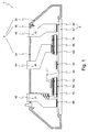
- Fig. 1 shows an inventive arrangement in an embodiment of a power semiconductor module.
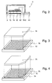
- FIG. 2 shows an arrangement according to the invention in the embodiment of a single, housed power semiconductor component.
- FIG. 3 shows a three-dimensional representation of a first arrangement of a metal molding on a power semiconductor component.
- FIG. 4 shows, in a three-dimensional representation, a second arrangement of a shaped metal body on a power semiconductor component.
- Fig. 5 shows steps of the manufacturing method according to the invention.
- FIG. 1 shows an arrangement (1), here a power semiconductor module, having a housing (3) which has a frame-like housing part (32) and a cover (34) with latching lugs (36) for snap-latching connection to the frame-like housing part (FIG. 32).
- the frame-like housing part (32) encloses a substrate (5).
- This has an insulating body (52), preferably an insulating ceramic, such as aluminum oxide or aluminum nitrite, and on the interior of the power semiconductor module facing first major surface on a self-structured Kupferkaschtechnik.
- the individual sections of this copper lamination form the conductor tracks (54) of the power semiconductor module.
- Power semiconductor components (70), connection elements (42, 44, 46) for load connections and connecting elements (40) are arranged on these conductor tracks (54). All these components are connected by solder joints with the tracks (54).
- the load connection elements (42, 44, 46) serve for the external connection of the power semiconductor components (70)
- the connection elements (40) serve for the circuit-compatible internal connection of the power semiconductor components (70).
- This metal shaped body (76) is preferably made of copper and is provided in the region of the pressure sintered connection with a galvanically applied noble metal surface. This metal shaped body (76) is connected by soldering to a connecting element (40). This is a particular advantage of pressure sintered connections, which allow even at higher temperatures, for example in the range of 300 ° C still a permanently secure electrical connection with high mechanical stability. Thus, subsequent executed connections such as solder, bond or other pressure sintered connections with this composite of power semiconductor device (70) and metal moldings (76) are possible.
- This combination of power semiconductor component (70) and metal shaped body (76) is particularly advantageous, since the current injection into the power semiconductor component (70) takes place uniformly over the entire contact area for bonding or non-planar solder joints by means of this metal shaped body (76) and thus the power semiconductor component (FIG. 70) is loaded homogeneously over its extension, which provides improved performance and reliability.
- FIG. 2 shows an arrangement (1) according to the invention in the form of a single power semiconductor component (70), which is modeled in so-called "TO" packages by way of example.
- a substrate (5) in this case a planar metal body which is simultaneously formed as a load connection element (42), the power semiconductor component (70), a further connection element (44) and a housing covering the substrate (3).
- the substrate (5) is electrically conductively connected to the power semiconductor device (70) by means of a pressure sintered connection.
- a metal shaped body (76) is arranged on the first main surface of the power semiconductor component (70) facing away from the substrate (5).
- the second load connection element (44) is connected by means of a third pressure sintered connection or by means of a soldered or glued connection.
- FIG. 3 shows, in a three-dimensional representation, a first arrangement of a metal molding (76) on an uncontrolled power semiconductor component (70), here a power diode.
- the power diode (70) has a contact surface (72) on its first main surface.
- This contact surface (72) has a multilayer metallization structure, wherein the uppermost layer consists of a noble metal, since this is necessary for a pressure sintered connection.
- a metal shaped body (76) with the lateral expansions of the contact surface (76) is arranged on this power semiconductor component (70) for reasons of clarity, and electrically conductively connected thereto by means of a pressure sintered connection.
- the metal molding (76) is formed as a cuboid made of copper or molybdenum or of an alloy containing these two metals to at least 80 of 100 parts by volume.
- the metal moldings (76) on a noble metal layer which corresponds at least to the size of the contact surface (72) of the power semiconductor device (70).
- the entire metal moldings (76) is coated with a galvanically applied noble metal layer.
- the flat, cuboid-shaped, metal shaped body (76) has a thickness of maximum 50 of 100 of its greatest lateral extent.
- the composite of power semiconductor component (70) and arranged by means of pressure sintering metal moldings (76) can be connected in circuits with Drucktern-, solder, adhesive or other pressure sintered connections circuit.
- FIG. 4 shows, in a three-dimensional representation, a second arrangement of a shaped metal body (76) on a power semiconductor component (70), here a controlled power switch, for example an IGBT (insulated gate bipolar transistor).
- the first main surface of the power semiconductor device (70) in this case has two contact surfaces (72, 74), a large area (72) for load connection and a further contact surface (74) lesser extent to the control connection.
- the contact surface (74) for the control connection is not covered by the associated metal shaped body (76) and can thus be connected, for example, by means of wire bonding technology according to the prior art.
- the metal molding (76) is therefore formed with a recess at a corner.
- Fig. 5 shows steps of the manufacturing method according to the invention.
- the starting point here is a plurality of power semiconductor components (70) in the wafer composite on a carrier film (90) arranged in a frame (92).
- Each power semiconductor component (70) has at least one contact surface on the first main surface facing away from the carrier film. This contact surface in turn has an uppermost metallization layer of a noble metal.
- a pasty layer of a metal powder and a solvent is selectively applied to a plurality of contact surfaces of the power semiconductor components.
- spraying (80) through a spray mask or the screen printing of the paste is particularly preferred.
- the metal moldings (76) are arranged on the contact surfaces of the power semiconductor components (70). It is here particularly preferred when the metal moldings (76) in the composite, so a plurality are arranged simultaneously.
- the metal moldings (76) can be connected to each other by means of webs (78) or the metal moldings (76) themselves are also arranged on a carrier material, similar to the carrier film (90) of the power semiconductor components (70).
- the pasty layer is dried either before or after this production step of applying the metal moldings (76).
- the simultaneous pressurization (82) takes place on a plurality of power semiconductor components (70) with metal moldings (76) arranged thereon for their respective sintered connection.
- the power semiconductor components (70) with metal moldings (76) arranged thereon preferably by means of sawing, isolated (84) and by known methods (86) are removed from the carrier film and arranged by way of example in a power semiconductor module.
Landscapes
- Die Bonding (AREA)
- Cooling Or The Like Of Semiconductors Or Solid State Devices (AREA)
Abstract
Description
- Die Erfindung beschreibt ein Verfahren zur Herstellung und eine Anordnung mit mindestens einem Leistungshalbleiterbauelement und mit einem Gehäuse, beispielhaft ausgestaltet als einzelnes gehaustes Leistungshalbleiterbauelement oder als Leistungshalbleitermodul mit einer Mehrzahl von schaltungsgerecht verbundenen Leistungshalbleiterbauelementen in einem Gehäuse. Einen Ausgangspunkt der Erfindung bilden somit Leistungshalbleitermodule wie sie beispielhaft aus der
DE 197 19 703 A1 und derEP 0 513 410 B1 bekannt sind - Derartige Leistungshalbleitermodule bestehen aus einem Gehäuse mit mindestens einem darin angeordneten elektrisch isolierenden Substrat vorzugsweise zur direkten Montage auf einem Kühlkörper. Das Substrat besteht aus einem Isolierstoffkörper mit einer Mehrzahl darauf befindlicher gegeneinander isolierter metallischer Verbindungsbahnen und hierauf befindlichen und mit diesen Verbindungsbahnen schaltungsgerecht verbundenen Leistungshalbleiterbauelementen. Weiterhin weist das Leistungshalbleitermodul Anschlusselemente für externe Last- und Hilfskontakte und in seinem Inneren angeordnete Verbindungselemente auf. Diese Verbindungselemente für schaltungsgerechte Verbindungen im Inneren des Leistungshalbleitermoduls sind meist als Drahtbondverbindungen (gemäß
DE 197 19 703 A1 ), oder als auf das Leistungshalbleiterbauelement gelötet Stanz- Biege- Teile (gemäßEP 0 513 410 B1 ) ausgebildete auf. - Nachteilig an Drahtbondverbindungen speziell für Leistungshalbleiterbauelemente mit hoher Stromtragfähigkeit pro Flächeneinheit ist, dass diese eine Vielzahl von Bonddrähten und jeder Bonddraht eine Mehrzahl von Bondfüßen aufweisen muss um die notwendigen Stromtragfähigkeit der Bondverbindung zu erreichen. Weiterhin nachteilig an Bondverbindungen ist, dass die elektrische Verbindung über eine Mehrzahl von voneinander beabstandeten Bondfüßen hergestellt wird und somit der Stromeintrag auf die Kontaktfläche dies Leistungshalbleiterbauelement nicht homogen erfolgt.
- Lötverbindungen eignen sich zur homogenen Stromeintrag auf die Kontaktflächen der Leistungshalbleiterbauelemente. Hierzu muss die Lötverbindung allerdings einen großen Teil der Kontaktfläche bedecken. Hierbei erweist sich die unterschiedliche thermische Ausdehnung des Leistungshalbleiterbauelement und des Verbindungselements als nachteilig. Dieser Nachteil wird gemindert durch relativ dicke Lotschichten, vorzugsweise aus hochbleihaltigem Lot, und durch den Einsatz von Trimetallverbindungselementen. Derartige Verbindungen weisen dann allerdings einen hohen elektrischen und thermischen Widerstand auf.
- Ebenfalls bekannt sind druckkontaktierte Leistungshalbleitermodule, wie sie beispielhaft aus der
DE 103 60 573 A1 bekannt sind. Hierbei ist zwischen einer Grundplatte und einem Druck einleitenden Element ein Leistungshalbleiterbauelement angeordnet. Derzeit sind druckkontaktierte Aufbauten, bei denen der Druck direkt auf das Leistungshalbleiterbauelement eingeleitet wird, besonders für Leistungsdioden und Leistungsthyristoren bekannt. Nachteilig an derartigen Aufbauten ist weiterhin, dass der Druck selektiv für jedes Leistungshalbleiterbauelement getrennt eingeleitet wird. - Den grundlegenden Stand der Technik für Verbindungen in Drucksintertechnik bildet die
DE 34 14 065 C2 . Diese offenbart ein Verfahren, das durch folgende wesentliche Verarbeitungsschritte gekennzeichnet ist: - Aufbringen einer aus einem Metallpulver und einem Lösungsmittel bestehenden pastösen Schicht auf die zu verbindende Kontaktfläche eines einzelnen Bauelements;
- Aufbringen des Bauelements auf ein Substrat, wobei die pastöse Schicht zwischen dem Bauelement und dem Substrat angeordnet wird;
- Austreiben des Lösungsmittels aus dem Verbund aus Bauelement, pastöser Schicht und Substrat;
- Erwärmung des Verbunds auf Sintertemperatur, unter zusätzlicher Druckbeaufschlagung.
- Bekannt ist weiterhin ein Verfahren gemäß
DE 10 2004 019 567 A1 , wobei dieses Verfahren den Vorteil aufweist für eine Mehrzahl von Leistungshalbleiterbauelementen die vorbereitenden Schritte der Drucksinterverbindung gleichzeitig durchführen zu können. Die eigentliche Sinterverbindung wird weiterhin selektiv für jedes Leistungshalbleiterbauelement einzeln ausgeführt. Das Verfahren weist die folgenden Schritte auf: - Aufbringen einer aus einem Metallpulver und einem Lösungsmittel bestehenden pastösen Schicht auf eine Trägerfolie;
- Trocknen der pastösen Schicht;
- Aufbringen von mindestens einem Bauelement auf die getrocknete Schicht;
- Druckbeaufschlagung des Verbunds aus dem mindestens einen Bauelement und der Trägerfolie mit der getrockneten Schicht, wodurch die Haftkraft zwischen der Schicht und dem Bauelement größer wird als zwischen der Schicht und der Trägerfolie;
- Abheben des mindestens einen Bauelements mit daran haftender Schicht von der Trägerfolie;
- Positionierung des Bauelements mit der daran haftenden Schicht auf dem Substrat;
- Druck- und Temperaturbeaufschlagung der Anordnung des Substrats und des Bauelements zu deren Sinterverbindung.
- Der Erfindung liegt die Aufgabe zugrunde eine Anordnung mit mindestens einem Leistungshalbleiterbauelement und mit einem Gehäuse vorzustellen, wobei die Stromeinleitung auf der dem Substrat abgewandten Seite des Leistungshalbleiterbauelements vollständig homogen erfolgt und weiterhin ein zugehöriges Herstellungsverfahren vorzustellen womit eine derartige Anordnung rationell hergestellt werden kann.
- Die Aufgabe wird erfindungsgemäß gelöst durch die Maßnahmen der Merkmale der Ansprüche 1 und 2. Bevorzugte Ausführungsformen sind in den Unteransprüchen beschrieben.
- Der erfinderische Gedanke bezieht sich auf eine Anordnung mit mindestens einem Leistungshalbleiterbauelement und einem elektrisch isolierenden Gehäuse. Diese Anordnung weist weiterhin nach außen führenden Anschlusselemente und mindestens ein vom Gehäuse zumindest teilweise umschlossenes Substrat auf. Auf der ersten Hauptfläche des Substrats ist die zweite Hauptfläche des mindestens einen Leistungshalbleiterbauelements angeordnet und elektrisch leitend verbunden.
- Auf seiner dem Substrat abgewandten ersten Hauptfläche weist das mindestens eine Leistungshalbleiterbauelement mindestens eine Kontaktfläche mit einer Metallisierungsschicht auf. Diese Metallisierungsschicht ist als Edelmetallschicht zur Drucksinterverbindung ausgebildet. Die Anordnung weist weiterhin einen Metallformkörper auf, dessen zweite Hauptfläche ebenfalls eine Edelmetallschicht aufweist. Dieser Metallformkörper ist mit einer der genannten Kontaktflächen des Leistungshalbleiterbauelements mittels einer Drucksinterverbindung verbunden.
- Das zugehörige Herstellungsverfahren geht aus von einer Mehrzahl von Leistungshalbleiterbauelementen im Waferverbund mit jeweils pro Leistungshalbleiterbauelement mindestens einer Kontaktfläche mit einer Metallisierungsschicht aus einem Edelmetall auf der ersten Hauptfläche. Das Verfahren weist mindestens die Schritte auf:
- Selektives Aufbringen einer aus einem Metallpulver, vorzugsweise Silber, und einem Lösungsmittel bestehenden pastösen Schicht auf die Kontaktflächen der Leistungshalbleiterbauelemente
- Trocknen der pastösen Schicht;
- Aufbringen von jeweils einem Metallformkörper auf die jeweilige getrocknete Schicht über der Kontaktfläche;
- Druckbeaufschlagung auf eine Mehrzahl von Leistungshalbleiterbauelementen mit darauf angeordneten Metallformkörpern zu deren Sinterverbindung;
- Vereinzelung der Leistungshalbleiterbauelemente aus dem Waferverbund;
- Anordnung der Leistungshalbleiterbauelemente mit Metallformkörper auf dem Substrat,
- Schaltungsgerechte Verbindung des Leistungshalbleiterbauelements mit darauf angeordnetem Metallformkörper mit weiteren Leistungshalbleiterbauelementen, Verbindungs- und / oder Anschlusselementen;
- Anordnung des Gehäuses.
- Die erfinderische Lösung wird an Hand der Ausführungsbeispiele der Fig. 1 bis 5 weiter erläutert.
- Fig. 1 zeigt eine erfindungsgemäße Anordnung in Ausgestaltung eines Leistungshalbleitermoduls.
- Fig. 2 zeigt eine erfindungsgemäße Anordnung in Ausgestaltung eines einzelnen gehausten Leistungshalbleiterbauelements.
- Fig. 3 zeigt in dreidimensionaler Darstellung eine erste Anordnung eines Metallformkörpers auf einem Leistungshalbleiterbauelement.
- Fig. 4 zeigt in dreidimensionaler Darstellung eine zweite Anordnung eines Metallformkörpers auf einem Leistungshalbleiterbauelement.
- Fig. 5 zeigt Schritte des erfindungsgemäßen Herstellungsverfahrens.
- Fig. 1 zeigt eine Anordnung (1), hier ein Leistungshalbleitermodul, mit einem Gehäuse (3), welches einen rahmenartigen Gehäuseteil (32) sowie einen Deckel (34) mit Rastnasen (36) zur Schnapp- Rast- Verbindung mit dem rahmenartigen Gehäuseteil (32), aufweist. Der rahmenartige Gehäuseteil (32) umschließt ein Substrat (5). Dieses weist einen Isolierstoffkörper (52), vorzugsweise eine lsolierkeramik, wie Aluminiumoxid oder Aluminiumnitrit, und auf deren dem Inneren des Leistungshalbleitermoduls zugewandten ersten Hauptfläche eine in sich strukturierte Kupferkaschierung auf. Die einzelnen Abschnitte dieser Kupferkaschierung bilden die Leiterbahnen (54) des Leistungshalbleitermoduls.
- Auf diesen Leiterbahnen (54) sind Leistungshalbleiterbauelemente (70), Anschlusselemente (42, 44, 46) für Lastanschlüsse und Verbindungselemente (40) angeordnet. All diese Komponenten sind mittels Lötverbindungen mit den Leiterbahnen (54) verbunden. Die Lastanschlusselement (42, 44, 46) dienen der externen Verbindung der Leistungshalbleiterbauelemente (70), die Verbindungselemente (40) dienen der schaltungsgerechten internen Verbindung der Leistungshalbleiterbauelemente (70).
- Die Leistungshalbleiterbauelemente (70), hier eine Leistungsdiode und ein Leistungsthyristor, weisen auf ihrer dem Substrat (5) abgewandten ersten Hauptfläche Kontaktflächen, vgl. Fig. 3 und 4, zur elektrischen Kontaktverbindung auf. Diese Kontaktflächen weisen eine zur Drucksinterverbindung geeignete Edelmetalloberfläche, vorzugsweise aus Gold, auf. Auf dieser Kontaktfläche und mit dieser mittels einer Drucksinterverbindung elektrisch leitend verbunden ist ein Metallformkörper (76) angeordnet.
- Dieser Metallformkörper (76) besteht vorzugsweise aus Kupfer und ist im Bereich der Drucksinterverbindung mit einer galvanisch aufgebrachten Edelmetalloberfläche versehen. Dieser Metallformkörper (76) ist mit einem Verbindungselement (40) löttechnisch verbunden. Hierin liegt ein besonderer Vorteil von Drucksinterverbindungen, die auch bei höheren Temperaturen, beispielhaft im Bereich um 300°C noch eine dauerhaft sichere elektrische Verbindung bei gleichzeitig hoher mechanischer Stabilität ermöglichen. Somit sind auch nachträgliche ausgeführte Verbindungen wie Löt-, Bond- oder weitere Drucksinterverbindungen mit diesem Verbund aus Leistungshalbleiterbauelement (70) und Metallformkörper (76) möglich.
- Besonders vorteilhaft ist dieser Verbund aus Leistungshalbleiterbauelement (70) und Metallformkörper (76), da bei Bond- oder nicht flächig ausgebildeten Lötverbindungen mittels dieses Metallformkörpers (76) die Stromeinprägung in das Leistungshalbleiterbauelement (70) gleichmäßig über die gesamte Kontaktfläche erfolgt und somit das Leistungshalbleiterbauelement (70) homogen über seine Ausdehnung belastet wird, was einer verbesserten Leistungsfähigkeit und höherer Zuverlässigkeit dient.
- Fig. 2 zeigt eine erfindungsgemäße Anordnung (1) in Ausgestaltung eines einzelnen, beispielhaft in sog. "TO-" Gehäusen, gehausten Leistungshalbleiterbauelements (70). Dargestellt ist ein Substrat (5), hier ein flächiger Metallkörper, der gleichzeitig als ein Lastanschlusselement (42) ausgebildet ist, das Leistungshalbleiterbauelement (70), ein weiteres Anschlusselement (44) und ein das Substrat überdeckendes Gehäuse (3).
- Das Substrat (5) ist mit dem Leistungshalbleiterbauelement (70) mittels einer Drucksinterverbindung elektrisch leitend verbunden. Mit einer ebensolchen Verbindung ist auf der ersten, dem Substrat (5) abgewandten Hauptfläche des Leistungshalbleiterbauelements (70), ein Metallformkörper (76) angeordnet. Auf diesem wiederum ist mittels einer dritten Drucksinterverbindung oder mittels einer Löt- oder Klebeverbindung das zweite Lastanschlusselement (44) verbunden.
- Fig. 3 zeigt in dreidimensionaler Darstellung eine erste Anordnung eines Metallformkörpers (76) auf einem ungesteuerten Leistungshalbleiterbauelement (70) hier einer Leistungsdiode. Die Leistungsdiode (70) weist hierzu auf ihrer ersten Hauptfläche eine Kontaktfläche (72) auf. Diese Kontaktfläche (72) weist eine mehrlagige Metallisierungsstruktur auf, wobei die oberste Lage aus einem Edelmetall besteht, da dies für eine Drucksinterverbindung notwendig ist.
- Auf diesem Leistungshalbleiterbauelement (70) aus Gründen der Übersichtlichkeit beabstandet dargestellt ist ein Metallformköper (76) mit den lateralen Ausdehnungen der Kontaktfläche (76) angeordnet und mit dieser mittels einer Drucksinterverbindung elektrisch leitend verbunden. Zur Ausgestaltung dieser Drucksinterverbindung vgl. Fig. 5. Der Metallformkörper (76) ist als Quader aus Kupfer oder Molybdän oder aus einer diese beiden Metalle zu mindestens 80 von 100 Volumenanteilen enthaltenden Legierung ausgebildet. Auf seiner zweiten dem Leistungshalbleiterbauelement (70) zugewandten Seite weist der Metallformkörper (76) eine Edelmetallschicht auf, die mindestens der Größe der Kontaktfläche (72) des Leistungshalbleiterbauelements (70) entspricht. Vorzugweise ist der gesamte Metallformkörper (76) mit einer galvanisch aufgebrachten Edelmetallschicht überzogen.
- Der flächige, quaderförmig ausgebildete, Metallformkörper (76) weist eine Dicke von maximalen 50 von 100 seiner größten lateralen Ausdehnung auf. Der Verbund aus Leistungshalbleiterbauelement (70) und mittels Drucksinterverfahren angeordnetem Metallformkörper (76) kann in Anordnungen mit Druckkontakt-, Löt-, Klebe- oder weiteren Drucksinterverbindungen schaltungsgerecht verbunden werden.
- Fig. 4 zeigt in dreidimensionaler Darstellung eine zweite Anordnung eines Metallformkörpers (76) auf einem Leistungshalbleiterbauelement (70) hier einem gesteuerten Leistungsschalter, beispielhaft einem IGBT (insulated gate bipolar transistor). Die erste Hauptfläche des Leistungshalbleiterbauelements (70) weist hierbei zwei Kontaktflächen (72, 74), eine großflächige (72) zur Lastverbindung und eine weitere Kontaktfläche (74) geringerer Ausdehnung zur Steuerverbindung auf. Die Kontaktfläche (74) zur Steuerverbindung wir hierbei durch den zugeordneten Metallformkörper (76) nicht abgedeckt und kann somit beispielhaft mittels Drahtbondtechnik nach dem Stand der Technik verbunden werden. Der Metallformkörper (76) ist daher mit einer Aussparung an einer Ecke ausgebildet.
- Fig. 5 zeigt Schritte des erfindungsgemäßen Herstellungsverfahrens. Ausgangspunkt hierbei sind eine Mehrzahl von Leistungshalbleiterbauelementen (70) im Waferverbund auf einer in einem Rahmen (92) angeordneten Trägerfolie (90). Jedes Leistungshalbleiterbauelement (70) weist mindestens eine Kontaktfläche auf der ersten, der Trägerfolie abgewandten Hauptfläche auf. Diese Kontaktfläche weist ihrerseits eine oberste Metallisierungsschicht aus einem Edelmetall auf.
- In einem ersten Schritt wird selektiv auf eine Mehrzahl Kontaktflächen der Leistungshalbleiterbauelemente eine pastöse Schicht aus einem Metallpulver und einem Lösungsmittel aufgebracht. Besonders bevorzugt ist hierbei das Aufsprühen (80) durch eine Sprühmaske oder der Siebdruck der Paste.
- In einem weiteren Schritt werden die Metallformkörper (76) auf den Kontaktflächen der Leistungshalbleiterbauelemente (70) angeordnet. Es ist hierbei besonders bevorzugt, wenn die Metallformkörper (76) im Verbund, also eine Mehrzahl gleichzeitig, angeordnet werden. Hierzu können die Metallformkörper (76) beispielhaft mittels Stegen (78) miteinander verbunden sein oder die Metallformkörper (76) sind selbst auch auf einem Trägermaterial, ähnlich der Trägerfolie (90) der Leistungshalbleiterbauelemente (70) angeordnet.
- Das Trocknen der pastösen Schicht erfolgt entweder vor oder nach diesem Herstellungsschritt des Aufbringens der Metallformkörper (76).
- Anschließend erfolgt die gleichzeitige Druckbeaufschlagung (82) auf eine Mehrzahl von Leistungshalbleiterbauelementen (70) mit darauf angeordneten Metallformkörpern (76) zu deren jeweiliger Sinterverbindung. In weiteren Prozessschritten werden die Leistungshalbleiterbauelemente (70) mit darauf angeordneten Metallformkörpern (76), vorzugsweise mittels Sägen, vereinzelt (84) und mit bekannten Verfahren (86) von der Trägerfolie abgenommen und beispielhaft in einem Leistungshalbleitermodul angeordnet.
Claims (9)
- Anordnung (1) mit mindestens einem Leistungshalbleiterbauelement (70) und einem elektrisch isolierenden Gehäuse (3), weiterhin mit nach außen führenden Anschlusselementen (42, 44, 46), mindestens einem vom Gehäuses (3) zumindest teilweise umschlossenen Substrat (5), wobei das mindestens eine Leistungshalbleiterbauelement (70) mit seiner zweiten Hauptfläche auf dem Substrat (5) angeordneten ist,
und wobei das mindestens eine Leistungshalbleiterbauelement (70) auf seiner dem Substrat (5) abgewandten ersten Hauptfläche mindestens eine Kontaktfläche mit einer Metallisierungsschicht aus einem Edelmetall aufweist und diese mindestens eine Kontaktfläche mit einem Metallformkörper (76) der auf seiner dem Leistungshalbleiterbauelement (70) zugewandeten zweiten Hauptfläche ebenfalls eine Edelmetallschicht aufweist, mittels einer Drucksinterverbindung miteinander verbunden ist. - Verfahren zur Herstellung einer Anordnung (1) gemäß Anspruch 1 ausgehend von einer Mehrzahl von Leistungshaibleiterbauelementen (70) im Waferverbund mit jeweils pro Leistungshalbleiterbauelement (70) mindestens einer Kontaktfläche mit einer Metallisierungsschicht (72) aus einem Edelmetall auf der ersten Hauptfläche, wobei das Verfahren mindestens die Schritte aufweist:a) Selektives Aufbringen (80) einer aus einem Metallpulver und einem Lösungsmittel bestehenden pastösen Schicht (20) auf die Kontaktflächen der Leistungshalbleiterbauelemente (70);b) Trocknen dieser pastösen Schicht (20);c) Aufbringen von jeweils einem Metallformkörper (76) auf die jeweilige getrocknete Schicht über der Kontaktfläche;d) Druckbeaufschlagung (82) auf eine Mehrzahl von Leistungshalbleiterbauelementen (70) mit darauf angeordneten Metallformkörpern (76) zu deren Sinterverbindung;e) Vereinzelung (84) der Leistungshalbleiterbauelemente (70) und der hiermit verbundenen Metallformkörper (76) aus dem Waferverbund;f) Anordnung der Leistungshalbleiterbauelemente (70) mit Metallformkörpern (76) auf dem Substrat (5);g) Schaltungsgerechte Verbindung des Leistungshalbleiterbauelement (70) mit darauf angeordnetem Metallformkörper (76) mit weiteren Leistungshalbleiterbauelementen, Verbindungs- und / oder Anschlusselementen;h) Anordnung des Gehäuses.
- Anordnung (1) nach Anspruch 1
wobei der Metallformkörper (76) flächig ausgebildet ist und eine Dicke von maximalen 50 von 100 seiner größten lateralen Ausdehnung aufweist. - Anordnung (1) nach Anspruch 1,
wobei das Leistungshalbleiterbauelement (70) auf seiner ersten Hauptfläche eine mehrlagige Metallisierung aufweist. - Anordnung (1) nach Anspruch 1,
wobei der Metallformkörper (76) aus Kupfer oder Molybdän oder einer eines dieser beiden Metalle zu mindestens 80 von 100 Volumenanteilen besteht und seine Oberfläche eine galvanisch abgeschiedene Edelmetalloberfläche aufweist. - Anordnung (1) nach Anspruch 1,
wobei das Substrat (5) aus einer Schichtfolge mit einem flächigen, elektrisch isolierenden, Keramikkörper (54) und mindestens einer Metallschicht besteht, die auf der dem Leistungshalbleiterbauelement (70) zugewandten Seite in sich strukturiert ist und somit eine Mehrzahl elektrisch voneinander isolierter Leiterbahnen (52) ausbildet und mindestens ein Leistungshalbleiterbauelement (70) auf mindestens einer dieser Leiterbahnen (52) angeordnet und mittels Druckkontakt-, Löt-, Klebe- oder Drucksinterverbindung mit diesem elektrisch leitend verbunden ist. - Verfahren nach Anspruch 2
wobei der Teilschritt a) mittels eines Siebdruckverfahrens ausgeführt wird. - Verfahren nach Anspruch 2
wobei die einzelnen Metallformkörper (76) beim Teilschritt c) im Verbund angeordnet sind. - Verfahren nach Anspruch 2
wobei der Teilschritt e) mittels eines Sägeverfahrens ausgeführt wird.
Applications Claiming Priority (1)
| Application Number | Priority Date | Filing Date | Title |
|---|---|---|---|
| DE102005047566A DE102005047566C5 (de) | 2005-10-05 | 2005-10-05 | Anordnung mit einem Leistungshalbleiterbauelement und mit einem Gehäuse sowie Herstellungsverfahren hierzu |
Publications (3)
| Publication Number | Publication Date |
|---|---|
| EP1772900A2 true EP1772900A2 (de) | 2007-04-11 |
| EP1772900A3 EP1772900A3 (de) | 2008-07-16 |
| EP1772900B1 EP1772900B1 (de) | 2012-04-25 |
Family
ID=37603438
Family Applications (1)
| Application Number | Title | Priority Date | Filing Date |
|---|---|---|---|
| EP06020799A Not-in-force EP1772900B1 (de) | 2005-10-05 | 2006-10-04 | Herstellungsverfahren einer Anordnung mit Leistungshalbleiterbauelementen, welches einen Schritt Drucksintern beinhaltet |
Country Status (5)
| Country | Link |
|---|---|
| EP (1) | EP1772900B1 (de) |
| JP (1) | JP5193452B2 (de) |
| AT (1) | ATE555498T1 (de) |
| DE (1) | DE102005047566C5 (de) |
| DK (1) | DK1772900T3 (de) |
Cited By (11)
| Publication number | Priority date | Publication date | Assignee | Title |
|---|---|---|---|---|
| WO2009019091A1 (de) * | 2007-08-09 | 2009-02-12 | Robert Bosch Gmbh | Baugruppe sowie herstellung einer baugruppe |
| EP2019421A3 (de) * | 2007-07-26 | 2012-10-31 | SEMIKRON Elektronik GmbH & Co. KG | Leistungshalbleiterbauelement mit Metallkontaktschicht sowie Herstellungsverfahren hierzu |
| WO2013053420A1 (de) * | 2011-10-15 | 2013-04-18 | Danfoss Silicon Power Gmbh | Leistungshalbleiterchip mit metallischen formkörpern zum kontaktieren mit dickdrähten oder bändchen sowie verfahren zu dessen herstellung |
| WO2013053419A1 (de) * | 2011-10-15 | 2013-04-18 | Danfoss Silicon Power Gmbh | Verfahren zur schaffung einer verbindung zwischen metallischen formköpern und einem leistungshalbleiterchip, die zur verbindung mit dickdrähten oder bändchen dienen |
| DE102012202281A1 (de) * | 2012-02-15 | 2013-08-22 | Infineon Technologies Ag | Halbleiteranordnung für Druckkontaktierung |
| DE102012212249A1 (de) * | 2012-07-12 | 2014-01-16 | Infineon Technologies Ag | Verfahren zur Herstellung eines Verbundes und eines Halbleitermoduls |
| WO2016005146A1 (de) * | 2014-07-11 | 2016-01-14 | Heraeus Deutschland Gmbh | Verfahren zum herstellen eines substratadapters, substratadapter und verfahren zum kontaktieren eines halbleiterelements |
| CN105632951A (zh) * | 2014-11-25 | 2016-06-01 | 贺利氏德国有限及两合公司 | 具有衬底适配器的半导体元件及其制造方法和其接触方法 |
| WO2016155965A3 (de) * | 2015-03-30 | 2016-11-24 | Robert Bosch Gmbh | Kontaktanordnung und verfahren zu herstellung der kontaktanordnung |
| US10607962B2 (en) | 2015-08-14 | 2020-03-31 | Danfoss Silicon Power Gmbh | Method for manufacturing semiconductor chips |
| US10847494B2 (en) | 2016-10-06 | 2020-11-24 | Agile Power Switch 3D-Integration Apsi3D | Method of determining thermal impedance of a sintering layer and a measurement system |
Families Citing this family (12)
| Publication number | Priority date | Publication date | Assignee | Title |
|---|---|---|---|---|
| US8164176B2 (en) * | 2006-10-20 | 2012-04-24 | Infineon Technologies Ag | Semiconductor module arrangement |
| DE102007022336A1 (de) * | 2007-05-12 | 2008-11-20 | Semikron Elektronik Gmbh & Co. Kg | Leistungshalbleitersubstrat mit Metallkontaktschicht sowie Herstellungsverfahren hierzu |
| EP2144284A1 (de) * | 2008-07-11 | 2010-01-13 | Siemens Aktiengesellschaft | Verfahren zum Herstellen eines Anschlusskontaktes an einem Halbleiterbauelement für die Leistungselektronik und elektronisches Bauteil mit einem auf diese Weise an einem Halblei-terbauelement hergestellten Anschlusskontakt |
| DE102008033410B4 (de) * | 2008-07-16 | 2011-06-30 | SEMIKRON Elektronik GmbH & Co. KG, 90431 | Leistungselektronische Verbindungseinrichtung mit einem Leistungshalbleiterbauelement und Herstellungsverfahren hierzu |
| DE102008055134A1 (de) * | 2008-12-23 | 2010-07-01 | Robert Bosch Gmbh | Elektrisches oder elektronisches Verbundbauteil sowie Verfahren zum Herstellen eines elektrischen oder elektronischen Verbundbauteils |
| DE102008055137A1 (de) * | 2008-12-23 | 2010-07-01 | Robert Bosch Gmbh | Elektrisches oder elektronisches Verbundbauteil sowie Verfahren zum Herstellen eines elektrischen oder elektronischen Verbundbauteils |
| JP5664028B2 (ja) * | 2010-08-31 | 2015-02-04 | 富士通株式会社 | 電子装置の製造方法 |
| DE112012007149B4 (de) | 2012-11-20 | 2020-07-09 | Denso Corporation | Halbleitervorrichtung |
| DE102014117246B4 (de) * | 2014-11-25 | 2018-11-15 | Heraeus Deutschland GmbH & Co. KG | Verfahren zum Herstellen eines Substratadapters, Substratadapter und Verfahren zum Kontaktieren eines Halbleiterelements |
| DE112017003925B4 (de) | 2016-08-05 | 2022-12-22 | Mitsubishi Electric Corporation | Leistungs-Halbleiterelement |
| DE102016121801B4 (de) * | 2016-11-14 | 2022-03-17 | Infineon Technologies Ag | Baugruppe mit Verbindungen, die verschiedene Schmelztemperaturen aufweisen, Fahrzeug mit der Baugruppe und Verfahren zum Herstellen derselben und Verwendung der Baugruppe für eine Automobilanwendung |
| DE102023113073B4 (de) | 2023-05-17 | 2025-12-24 | Semikron Danfoss Elektronik Gmbh & Co. Kg | Leistungshalbleiterbauelement mit Kontakteinrichtung und Herstellungsverfahren hierfür |
Citations (1)
| Publication number | Priority date | Publication date | Assignee | Title |
|---|---|---|---|---|
| US5499178A (en) | 1991-12-16 | 1996-03-12 | Regents Of The University Of Minnesota | System for reducing harmonics by harmonic current injection |
Family Cites Families (15)
| Publication number | Priority date | Publication date | Assignee | Title |
|---|---|---|---|---|
| DE1263190B (de) * | 1961-07-12 | 1968-03-14 | Siemens Ag | Halbleiteranordnung mit einem in ein Gehaeuse eingeschlossenen Halbleiterkoerper |
| DE3414065A1 (de) * | 1984-04-13 | 1985-12-12 | Siemens AG, 1000 Berlin und 8000 München | Anordnung bestehend aus mindestens einem auf einem substrat befestigten elektronischen bauelement und verfahren zur herstellung einer derartigen anordnung |
| DE4040753A1 (de) * | 1990-12-19 | 1992-06-25 | Siemens Ag | Leistungshalbleiterbauelement |
| DE59100737D1 (de) * | 1991-05-15 | 1994-01-27 | Abb Ixys Semiconductor Gmbh | Leistungshalbleitermodul und Verfahren zur Herstellung eines solchen Moduls. |
| DE4300516C2 (de) * | 1993-01-12 | 2001-05-17 | Ixys Semiconductor Gmbh | Leistungshalbleitermodul |
| DE19612838A1 (de) * | 1995-11-13 | 1997-05-15 | Asea Brown Boveri | Leistungshalbleiterbauelement sowie Verfahren zu dessen Herstellung |
| DE19719703C5 (de) * | 1997-05-09 | 2005-11-17 | eupec Europäische Gesellschaft für Leistungshalbleiter mbH & Co. KG | Leistungshalbleitermodul mit Keramiksubstrat |
| JP3220900B2 (ja) * | 1997-06-24 | 2001-10-22 | 三菱電機株式会社 | パワー半導体モジュール |
| DE19739684B4 (de) * | 1997-09-10 | 2006-04-13 | Robert Bosch Gmbh | Verfahren zur Herstellung von Chipstapeln |
| DE10062108B4 (de) * | 2000-12-13 | 2010-04-15 | Infineon Technologies Ag | Leistungsmodul mit verbessertem transienten Wärmewiderstand |
| DE10222609B4 (de) * | 2002-04-15 | 2008-07-10 | Schott Ag | Verfahren zur Herstellung strukturierter Schichten auf Substraten und verfahrensgemäß beschichtetes Substrat |
| DE10303103B4 (de) * | 2003-01-28 | 2009-07-09 | Ixys Semiconductor Gmbh | Halbleiterbauteil, insbesondere Leistungshalbleiterbauteil |
| DE10360573B4 (de) * | 2003-12-22 | 2008-02-14 | Infineon Technologies Ag | Leistungshalbleitermodul |
| DE102004019567B3 (de) * | 2004-04-22 | 2006-01-12 | Semikron Elektronik Gmbh & Co. Kg | Verfahren zur Befestigung von elektronischen Bauelementen auf einem Substrat |
| DE102004056702B3 (de) * | 2004-04-22 | 2006-03-02 | Semikron Elektronik Gmbh & Co. Kg | Verfahren zur Befestigung von elektronischen Bauelementen auf einem Substrat |
-
2005
- 2005-10-05 DE DE102005047566A patent/DE102005047566C5/de not_active Expired - Fee Related
-
2006
- 2006-10-04 AT AT06020799T patent/ATE555498T1/de active
- 2006-10-04 DK DK06020799.0T patent/DK1772900T3/da active
- 2006-10-04 JP JP2006272883A patent/JP5193452B2/ja not_active Expired - Fee Related
- 2006-10-04 EP EP06020799A patent/EP1772900B1/de not_active Not-in-force
Patent Citations (1)
| Publication number | Priority date | Publication date | Assignee | Title |
|---|---|---|---|---|
| US5499178A (en) | 1991-12-16 | 1996-03-12 | Regents Of The University Of Minnesota | System for reducing harmonics by harmonic current injection |
Cited By (22)
| Publication number | Priority date | Publication date | Assignee | Title |
|---|---|---|---|---|
| EP2019421A3 (de) * | 2007-07-26 | 2012-10-31 | SEMIKRON Elektronik GmbH & Co. KG | Leistungshalbleiterbauelement mit Metallkontaktschicht sowie Herstellungsverfahren hierzu |
| US9233436B2 (en) | 2007-08-09 | 2016-01-12 | Robert Bosch Gmbh | Assembly and production of an assembly |
| US8552306B2 (en) | 2007-08-09 | 2013-10-08 | Robert Bosch Gmbh | Assembly and production of an assembly |
| WO2009019091A1 (de) * | 2007-08-09 | 2009-02-12 | Robert Bosch Gmbh | Baugruppe sowie herstellung einer baugruppe |
| CN103890924B (zh) * | 2011-10-15 | 2017-02-15 | 丹佛斯硅动力股份有限公司 | 具有用于接触厚布线或条片的金属成型体的功率半导体芯片及其制造方法 |
| US9318421B2 (en) | 2011-10-15 | 2016-04-19 | Danfoss Silicon Power Gmbh | Power semiconductor chip with a metallic moulded body for contacting thick wires or strips and method for the production thereof |
| CN103875067B (zh) * | 2011-10-15 | 2018-02-13 | 丹佛斯硅动力股份有限公司 | 在金属成型体和结合到厚布线或条片用的功率半导体间形成连接的方法 |
| CN103875067A (zh) * | 2011-10-15 | 2014-06-18 | 丹佛斯硅动力股份有限公司 | 在金属成型体和结合到厚布线或条片用的功率半导体间形成连接的方法 |
| CN103890924A (zh) * | 2011-10-15 | 2014-06-25 | 丹佛斯硅动力股份有限公司 | 具有用于接触厚布线或条片的金属成型体的功率半导体芯片及其制造方法 |
| EP2766925A1 (de) * | 2011-10-15 | 2014-08-20 | Danfoss Silicon Power GmbH | Verfahren zur schaffung einer verbindung zwischen metallischen formköpern und einem leistungshalbleiterchip, die zur verbindung mit dickdrähten oder bändchen dienen |
| WO2013053419A1 (de) * | 2011-10-15 | 2013-04-18 | Danfoss Silicon Power Gmbh | Verfahren zur schaffung einer verbindung zwischen metallischen formköpern und einem leistungshalbleiterchip, die zur verbindung mit dickdrähten oder bändchen dienen |
| WO2013053420A1 (de) * | 2011-10-15 | 2013-04-18 | Danfoss Silicon Power Gmbh | Leistungshalbleiterchip mit metallischen formkörpern zum kontaktieren mit dickdrähten oder bändchen sowie verfahren zu dessen herstellung |
| US9786627B2 (en) | 2011-10-15 | 2017-10-10 | Danfoss Silicon Power Gmbh | Method for creating a connection between metallic moulded bodies and a power semiconductor which is used to bond to thick wires or strips |
| DE102012202281A1 (de) * | 2012-02-15 | 2013-08-22 | Infineon Technologies Ag | Halbleiteranordnung für Druckkontaktierung |
| DE102012212249B4 (de) * | 2012-07-12 | 2016-02-25 | Infineon Technologies Ag | Verfahren zur Herstellung eines Verbundes und eines Halbleitermoduls |
| DE102012212249A1 (de) * | 2012-07-12 | 2014-01-16 | Infineon Technologies Ag | Verfahren zur Herstellung eines Verbundes und eines Halbleitermoduls |
| WO2016005146A1 (de) * | 2014-07-11 | 2016-01-14 | Heraeus Deutschland Gmbh | Verfahren zum herstellen eines substratadapters, substratadapter und verfahren zum kontaktieren eines halbleiterelements |
| CN105632951A (zh) * | 2014-11-25 | 2016-06-01 | 贺利氏德国有限及两合公司 | 具有衬底适配器的半导体元件及其制造方法和其接触方法 |
| EP3026702A1 (de) * | 2014-11-25 | 2016-06-01 | Heraeus Deutschland GmbH & Co. KG | Verfahren zum herstellen eines halbleiterelements mit substratadapter, halbleiterelement mit substratadapter und verfahren zum kontaktieren eines halbleiterelements |
| WO2016155965A3 (de) * | 2015-03-30 | 2016-11-24 | Robert Bosch Gmbh | Kontaktanordnung und verfahren zu herstellung der kontaktanordnung |
| US10607962B2 (en) | 2015-08-14 | 2020-03-31 | Danfoss Silicon Power Gmbh | Method for manufacturing semiconductor chips |
| US10847494B2 (en) | 2016-10-06 | 2020-11-24 | Agile Power Switch 3D-Integration Apsi3D | Method of determining thermal impedance of a sintering layer and a measurement system |
Also Published As
| Publication number | Publication date |
|---|---|
| DE102005047566C5 (de) | 2011-06-09 |
| DE102005047566B4 (de) | 2009-05-14 |
| EP1772900A3 (de) | 2008-07-16 |
| ATE555498T1 (de) | 2012-05-15 |
| DE102005047566A1 (de) | 2007-04-12 |
| DK1772900T3 (da) | 2012-07-23 |
| JP5193452B2 (ja) | 2013-05-08 |
| EP1772900B1 (de) | 2012-04-25 |
| JP2007103949A (ja) | 2007-04-19 |
Similar Documents
| Publication | Publication Date | Title |
|---|---|---|
| EP1772900B1 (de) | Herstellungsverfahren einer Anordnung mit Leistungshalbleiterbauelementen, welches einen Schritt Drucksintern beinhaltet | |
| DE112014001487B4 (de) | Halbleitermodul | |
| DE102009044641B4 (de) | Einrichtung mit einem Halbleiterchip und Metallfolie sowie ein Verfahren zur Herstellung der Einrichtung | |
| DE102009017853B4 (de) | Verfahren zur Herstellung einer Halbleitervorrichtung | |
| DE102009039227B4 (de) | Verfahren zur Herstellung eines Halbleiterbauelements | |
| DE102010037439B4 (de) | Bauelement mit einem Halbleiterchip und einem Träger und Fabrikationsverfahren | |
| EP1956647A1 (de) | Schaltungsanordnung mit Verbindungseinrichtung sowie Herstellungsverfahren hierzu | |
| DE102016206542B4 (de) | Verfahren zum Herstellen einer Halbleitervorrichtung | |
| DE102009000587A1 (de) | Modul mit einer gesinterten Verbindung zwischen einem Halbleiterchip und einer Kupferoberfläche und Verfahren zur Herstellung eines Moduls mit einer gesinterten Verbindung zwischen einem Halbleiterchip und einer Kupferoberfläche | |
| DE102009026480A1 (de) | Modul mit einer gesinterten Fügestelle | |
| DE102004041088B4 (de) | Halbleiterbauteil in Flachleitertechnik mit einem Halbleiterchip und Verfahren zu seiner Herstellung | |
| DE102015109186A1 (de) | Halbleiteranordnung, Halbleitersystem und Verfahren zur Ausbildung einer Halbleiteranordnung | |
| DE102004057421B4 (de) | Druckkontaktiertes Leistungshalbleitermodul für hohe Umgebungstemperaturen und Verfahren zu seiner Herstellung | |
| DE102009018541A1 (de) | Kontaktierungsmittel und Verfahren zur Kontaktierung elektrischer Bauteile | |
| DE102005047567B3 (de) | Leistungshalbleitermodul mit Isolationszwischenlage und Verfahren zu seiner Herstellung | |
| EP3300105B1 (de) | Leistungshalbleitermodul und verfahren zur herstellung eines leistungshalbleitermoduls | |
| DE102015107109B4 (de) | Elektronische Vorrichtung mit einem Metallsubstrat und einem in einem Laminat eingebetteten Halbleitermodul | |
| DE102005050534B4 (de) | Leistungshalbleitermodul | |
| DE102014105367B4 (de) | Pressmasse und Verfahren zum Verpacken von Halbleiterchips | |
| WO2018037047A1 (de) | Leistungsmodul, verfahren zur herstellung und leistungselektronikschaltung | |
| DE102014203306A1 (de) | Herstellen eines Elektronikmoduls | |
| EP1993132A2 (de) | Leistungshalbleitersubstrat mit Metallkontaktschicht sowie Herstellungsverfahren hierzu | |
| DE102008040290A1 (de) | Hybridschaltungsstruktur mit keramischen Schaltungsträgern | |
| DE102014111930A1 (de) | Thermisch gut leitendes, elektrisch isolierendes Gehäuse mit elektronischen Bauelementen und Herstellverfahren | |
| WO2022028915A1 (de) | Elektronisches schaltungsmodul |
Legal Events
| Date | Code | Title | Description |
|---|---|---|---|
| PUAI | Public reference made under article 153(3) epc to a published international application that has entered the european phase |
Free format text: ORIGINAL CODE: 0009012 |
|
| AK | Designated contracting states |
Kind code of ref document: A2 Designated state(s): AT BE BG CH CY CZ DE DK EE ES FI FR GB GR HU IE IS IT LI LT LU LV MC NL PL PT RO SE SI SK TR |
|
| AX | Request for extension of the european patent |
Extension state: AL BA HR MK YU |
|
| PUAL | Search report despatched |
Free format text: ORIGINAL CODE: 0009013 |
|
| AK | Designated contracting states |
Kind code of ref document: A3 Designated state(s): AT BE BG CH CY CZ DE DK EE ES FI FR GB GR HU IE IS IT LI LT LU LV MC NL PL PT RO SE SI SK TR |
|
| AX | Request for extension of the european patent |
Extension state: AL BA HR MK RS |
|
| RIC1 | Information provided on ipc code assigned before grant |
Ipc: H01L 21/60 20060101AFI20070122BHEP Ipc: H01L 23/492 20060101ALI20080606BHEP Ipc: H01L 25/07 20060101ALI20080606BHEP |
|
| 17P | Request for examination filed |
Effective date: 20080707 |
|
| 17Q | First examination report despatched |
Effective date: 20080826 |
|
| AKX | Designation fees paid |
Designated state(s): AT BE BG CH CY CZ DE DK EE ES FI FR GB GR HU IE IS IT LI LT LU LV MC NL PL PT RO SE SI SK TR |
|
| REG | Reference to a national code |
Ref country code: DE Ref legal event code: R079 Ref document number: 502006011340 Country of ref document: DE Free format text: PREVIOUS MAIN CLASS: H01L0021600000 Ipc: H01L0021980000 |
|
| RIC1 | Information provided on ipc code assigned before grant |
Ipc: H01L 25/07 20060101ALI20111114BHEP Ipc: H01L 23/492 20060101ALI20111114BHEP Ipc: H01L 21/60 20060101ALI20111114BHEP Ipc: H01L 21/98 20060101AFI20111114BHEP |
|
| RTI1 | Title (correction) |
Free format text: FABRICATION METHOD OF A DEVICE WITH POWER SEMICONDUCTOR COMPONENTS INCLUDING A PRESSURE SINTERING STEP |
|
| GRAP | Despatch of communication of intention to grant a patent |
Free format text: ORIGINAL CODE: EPIDOSNIGR1 |
|
| GRAS | Grant fee paid |
Free format text: ORIGINAL CODE: EPIDOSNIGR3 |
|
| GRAA | (expected) grant |
Free format text: ORIGINAL CODE: 0009210 |
|
| AK | Designated contracting states |
Kind code of ref document: B1 Designated state(s): AT BE BG CH CY CZ DE DK EE ES FI FR GB GR HU IE IS IT LI LT LU LV MC NL PL PT RO SE SI SK TR |
|
| REG | Reference to a national code |
Ref country code: GB Ref legal event code: FG4D Free format text: NOT ENGLISH |
|
| REG | Reference to a national code |
Ref country code: CH Ref legal event code: EP |
|
| REG | Reference to a national code |
Ref country code: CH Ref legal event code: NV Representative=s name: BRAUNPAT BRAUN EDER AG Ref country code: AT Ref legal event code: REF Ref document number: 555498 Country of ref document: AT Kind code of ref document: T Effective date: 20120515 |
|
| REG | Reference to a national code |
Ref country code: IE Ref legal event code: FG4D Free format text: LANGUAGE OF EP DOCUMENT: GERMAN |
|
| REG | Reference to a national code |
Ref country code: DE Ref legal event code: R096 Ref document number: 502006011340 Country of ref document: DE Effective date: 20120614 |
|
| REG | Reference to a national code |
Ref country code: DK Ref legal event code: T3 |
|
| REG | Reference to a national code |
Ref country code: SE Ref legal event code: TRGR |
|
| REG | Reference to a national code |
Ref country code: NL Ref legal event code: VDEP Effective date: 20120425 |
|
| REG | Reference to a national code |
Ref country code: SK Ref legal event code: T3 Ref document number: E 11879 Country of ref document: SK |
|
| LTIE | Lt: invalidation of european patent or patent extension |
Effective date: 20120425 |
|
| PG25 | Lapsed in a contracting state [announced via postgrant information from national office to epo] |
Ref country code: FI Free format text: LAPSE BECAUSE OF FAILURE TO SUBMIT A TRANSLATION OF THE DESCRIPTION OR TO PAY THE FEE WITHIN THE PRESCRIBED TIME-LIMIT Effective date: 20120425 Ref country code: CY Free format text: LAPSE BECAUSE OF FAILURE TO SUBMIT A TRANSLATION OF THE DESCRIPTION OR TO PAY THE FEE WITHIN THE PRESCRIBED TIME-LIMIT Effective date: 20120425 Ref country code: IS Free format text: LAPSE BECAUSE OF FAILURE TO SUBMIT A TRANSLATION OF THE DESCRIPTION OR TO PAY THE FEE WITHIN THE PRESCRIBED TIME-LIMIT Effective date: 20120825 Ref country code: LT Free format text: LAPSE BECAUSE OF FAILURE TO SUBMIT A TRANSLATION OF THE DESCRIPTION OR TO PAY THE FEE WITHIN THE PRESCRIBED TIME-LIMIT Effective date: 20120425 Ref country code: PL Free format text: LAPSE BECAUSE OF FAILURE TO SUBMIT A TRANSLATION OF THE DESCRIPTION OR TO PAY THE FEE WITHIN THE PRESCRIBED TIME-LIMIT Effective date: 20120425 |
|
| PG25 | Lapsed in a contracting state [announced via postgrant information from national office to epo] |
Ref country code: SI Free format text: LAPSE BECAUSE OF FAILURE TO SUBMIT A TRANSLATION OF THE DESCRIPTION OR TO PAY THE FEE WITHIN THE PRESCRIBED TIME-LIMIT Effective date: 20120425 Ref country code: GR Free format text: LAPSE BECAUSE OF FAILURE TO SUBMIT A TRANSLATION OF THE DESCRIPTION OR TO PAY THE FEE WITHIN THE PRESCRIBED TIME-LIMIT Effective date: 20120726 Ref country code: PT Free format text: LAPSE BECAUSE OF FAILURE TO SUBMIT A TRANSLATION OF THE DESCRIPTION OR TO PAY THE FEE WITHIN THE PRESCRIBED TIME-LIMIT Effective date: 20120827 Ref country code: LV Free format text: LAPSE BECAUSE OF FAILURE TO SUBMIT A TRANSLATION OF THE DESCRIPTION OR TO PAY THE FEE WITHIN THE PRESCRIBED TIME-LIMIT Effective date: 20120425 |
|
| PG25 | Lapsed in a contracting state [announced via postgrant information from national office to epo] |
Ref country code: EE Free format text: LAPSE BECAUSE OF FAILURE TO SUBMIT A TRANSLATION OF THE DESCRIPTION OR TO PAY THE FEE WITHIN THE PRESCRIBED TIME-LIMIT Effective date: 20120425 Ref country code: NL Free format text: LAPSE BECAUSE OF FAILURE TO SUBMIT A TRANSLATION OF THE DESCRIPTION OR TO PAY THE FEE WITHIN THE PRESCRIBED TIME-LIMIT Effective date: 20120425 Ref country code: CZ Free format text: LAPSE BECAUSE OF FAILURE TO SUBMIT A TRANSLATION OF THE DESCRIPTION OR TO PAY THE FEE WITHIN THE PRESCRIBED TIME-LIMIT Effective date: 20120425 Ref country code: RO Free format text: LAPSE BECAUSE OF FAILURE TO SUBMIT A TRANSLATION OF THE DESCRIPTION OR TO PAY THE FEE WITHIN THE PRESCRIBED TIME-LIMIT Effective date: 20120425 |
|
| PG25 | Lapsed in a contracting state [announced via postgrant information from national office to epo] |
Ref country code: IT Free format text: LAPSE BECAUSE OF FAILURE TO SUBMIT A TRANSLATION OF THE DESCRIPTION OR TO PAY THE FEE WITHIN THE PRESCRIBED TIME-LIMIT Effective date: 20120425 |
|
| PLBE | No opposition filed within time limit |
Free format text: ORIGINAL CODE: 0009261 |
|
| STAA | Information on the status of an ep patent application or granted ep patent |
Free format text: STATUS: NO OPPOSITION FILED WITHIN TIME LIMIT |
|
| 26N | No opposition filed |
Effective date: 20130128 |
|
| BERE | Be: lapsed |
Owner name: SEMIKRON ELEKTRONIK G.M.B.H. & CO. KG PATENTABTEI Effective date: 20121031 |
|
| PG25 | Lapsed in a contracting state [announced via postgrant information from national office to epo] |
Ref country code: ES Free format text: LAPSE BECAUSE OF FAILURE TO SUBMIT A TRANSLATION OF THE DESCRIPTION OR TO PAY THE FEE WITHIN THE PRESCRIBED TIME-LIMIT Effective date: 20120805 |
|
| REG | Reference to a national code |
Ref country code: DE Ref legal event code: R097 Ref document number: 502006011340 Country of ref document: DE Effective date: 20130128 |
|
| PG25 | Lapsed in a contracting state [announced via postgrant information from national office to epo] |
Ref country code: MC Free format text: LAPSE BECAUSE OF NON-PAYMENT OF DUE FEES Effective date: 20121031 |
|
| REG | Reference to a national code |
Ref country code: IE Ref legal event code: MM4A |
|
| PG25 | Lapsed in a contracting state [announced via postgrant information from national office to epo] |
Ref country code: BE Free format text: LAPSE BECAUSE OF NON-PAYMENT OF DUE FEES Effective date: 20121031 Ref country code: IE Free format text: LAPSE BECAUSE OF NON-PAYMENT OF DUE FEES Effective date: 20121004 Ref country code: BG Free format text: LAPSE BECAUSE OF FAILURE TO SUBMIT A TRANSLATION OF THE DESCRIPTION OR TO PAY THE FEE WITHIN THE PRESCRIBED TIME-LIMIT Effective date: 20120725 |
|
| REG | Reference to a national code |
Ref country code: AT Ref legal event code: MM01 Ref document number: 555498 Country of ref document: AT Kind code of ref document: T Effective date: 20121031 |
|
| PG25 | Lapsed in a contracting state [announced via postgrant information from national office to epo] |
Ref country code: AT Free format text: LAPSE BECAUSE OF NON-PAYMENT OF DUE FEES Effective date: 20121031 |
|
| PG25 | Lapsed in a contracting state [announced via postgrant information from national office to epo] |
Ref country code: TR Free format text: LAPSE BECAUSE OF FAILURE TO SUBMIT A TRANSLATION OF THE DESCRIPTION OR TO PAY THE FEE WITHIN THE PRESCRIBED TIME-LIMIT Effective date: 20120425 |
|
| PG25 | Lapsed in a contracting state [announced via postgrant information from national office to epo] |
Ref country code: LU Free format text: LAPSE BECAUSE OF NON-PAYMENT OF DUE FEES Effective date: 20121004 |
|
| PG25 | Lapsed in a contracting state [announced via postgrant information from national office to epo] |
Ref country code: HU Free format text: LAPSE BECAUSE OF FAILURE TO SUBMIT A TRANSLATION OF THE DESCRIPTION OR TO PAY THE FEE WITHIN THE PRESCRIBED TIME-LIMIT Effective date: 20061004 |
|
| REG | Reference to a national code |
Ref country code: FR Ref legal event code: PLFP Year of fee payment: 10 |
|
| REG | Reference to a national code |
Ref country code: FR Ref legal event code: PLFP Year of fee payment: 11 |
|
| PGFP | Annual fee paid to national office [announced via postgrant information from national office to epo] |
Ref country code: SK Payment date: 20160928 Year of fee payment: 11 |
|
| PGFP | Annual fee paid to national office [announced via postgrant information from national office to epo] |
Ref country code: SE Payment date: 20161025 Year of fee payment: 11 |
|
| REG | Reference to a national code |
Ref country code: FR Ref legal event code: PLFP Year of fee payment: 12 |
|
| REG | Reference to a national code |
Ref country code: CH Ref legal event code: PCAR Free format text: NEW ADDRESS: HOLEESTRASSE 87, 4054 BASEL (CH) |
|
| REG | Reference to a national code |
Ref country code: SE Ref legal event code: EUG |
|
| REG | Reference to a national code |
Ref country code: SK Ref legal event code: MM4A Ref document number: E 11879 Country of ref document: SK Effective date: 20171004 |
|
| PG25 | Lapsed in a contracting state [announced via postgrant information from national office to epo] |
Ref country code: SK Free format text: LAPSE BECAUSE OF NON-PAYMENT OF DUE FEES Effective date: 20171004 |
|
| PG25 | Lapsed in a contracting state [announced via postgrant information from national office to epo] |
Ref country code: SE Free format text: LAPSE BECAUSE OF NON-PAYMENT OF DUE FEES Effective date: 20171005 |
|
| REG | Reference to a national code |
Ref country code: FR Ref legal event code: PLFP Year of fee payment: 13 |
|
| PGFP | Annual fee paid to national office [announced via postgrant information from national office to epo] |
Ref country code: GB Payment date: 20211022 Year of fee payment: 16 Ref country code: DK Payment date: 20211021 Year of fee payment: 16 Ref country code: DE Payment date: 20211031 Year of fee payment: 16 |
|
| PGFP | Annual fee paid to national office [announced via postgrant information from national office to epo] |
Ref country code: FR Payment date: 20211022 Year of fee payment: 16 Ref country code: CH Payment date: 20211022 Year of fee payment: 16 |
|
| REG | Reference to a national code |
Ref country code: DE Ref legal event code: R119 Ref document number: 502006011340 Country of ref document: DE |
|
| REG | Reference to a national code |
Ref country code: DK Ref legal event code: EBP Effective date: 20221031 |
|
| REG | Reference to a national code |
Ref country code: CH Ref legal event code: PL |
|
| GBPC | Gb: european patent ceased through non-payment of renewal fee |
Effective date: 20221004 |
|
| PG25 | Lapsed in a contracting state [announced via postgrant information from national office to epo] |
Ref country code: LI Free format text: LAPSE BECAUSE OF NON-PAYMENT OF DUE FEES Effective date: 20221031 Ref country code: FR Free format text: LAPSE BECAUSE OF NON-PAYMENT OF DUE FEES Effective date: 20221031 Ref country code: DE Free format text: LAPSE BECAUSE OF NON-PAYMENT OF DUE FEES Effective date: 20230503 Ref country code: CH Free format text: LAPSE BECAUSE OF NON-PAYMENT OF DUE FEES Effective date: 20221031 |
|
| PG25 | Lapsed in a contracting state [announced via postgrant information from national office to epo] |
Ref country code: GB Free format text: LAPSE BECAUSE OF NON-PAYMENT OF DUE FEES Effective date: 20221004 Ref country code: DK Free format text: LAPSE BECAUSE OF NON-PAYMENT OF DUE FEES Effective date: 20221031 |