EP1775709A2 - Elektroforesevorrichtung, elektronisches Gerät und Ansteuerverfahren für eine Elektroforesevorrichtung - Google Patents
Elektroforesevorrichtung, elektronisches Gerät und Ansteuerverfahren für eine Elektroforesevorrichtung Download PDFInfo
- Publication number
- EP1775709A2 EP1775709A2 EP06019571A EP06019571A EP1775709A2 EP 1775709 A2 EP1775709 A2 EP 1775709A2 EP 06019571 A EP06019571 A EP 06019571A EP 06019571 A EP06019571 A EP 06019571A EP 1775709 A2 EP1775709 A2 EP 1775709A2
- Authority
- EP
- European Patent Office
- Prior art keywords
- voltage
- common electrode
- pixel electrode
- potential
- pixel
- Prior art date
- Legal status (The legal status is an assumption and is not a legal conclusion. Google has not performed a legal analysis and makes no representation as to the accuracy of the status listed.)
- Withdrawn
Links
Images

Classifications
-
- G—PHYSICS
- G09—EDUCATION; CRYPTOGRAPHY; DISPLAY; ADVERTISING; SEALS
- G09G—ARRANGEMENTS OR CIRCUITS FOR CONTROL OF INDICATING DEVICES USING STATIC MEANS TO PRESENT VARIABLE INFORMATION
- G09G3/00—Control arrangements or circuits, of interest only in connection with visual indicators other than cathode-ray tubes
- G09G3/20—Control arrangements or circuits, of interest only in connection with visual indicators other than cathode-ray tubes for presentation of an assembly of a number of characters, e.g. a page, by composing the assembly by combination of individual elements arranged in a matrix no fixed position being assigned to or needed to be assigned to the individual characters or partial characters
- G09G3/34—Control arrangements or circuits, of interest only in connection with visual indicators other than cathode-ray tubes for presentation of an assembly of a number of characters, e.g. a page, by composing the assembly by combination of individual elements arranged in a matrix no fixed position being assigned to or needed to be assigned to the individual characters or partial characters by control of light from an independent source
- G09G3/3433—Control arrangements or circuits, of interest only in connection with visual indicators other than cathode-ray tubes for presentation of an assembly of a number of characters, e.g. a page, by composing the assembly by combination of individual elements arranged in a matrix no fixed position being assigned to or needed to be assigned to the individual characters or partial characters by control of light from an independent source using light modulating elements actuated by an electric field and being other than liquid crystal devices and electrochromic devices
- G09G3/344—Control arrangements or circuits, of interest only in connection with visual indicators other than cathode-ray tubes for presentation of an assembly of a number of characters, e.g. a page, by composing the assembly by combination of individual elements arranged in a matrix no fixed position being assigned to or needed to be assigned to the individual characters or partial characters by control of light from an independent source using light modulating elements actuated by an electric field and being other than liquid crystal devices and electrochromic devices based on particles moving in a fluid or in a gas, e.g. electrophoretic devices
-
- G—PHYSICS
- G09—EDUCATION; CRYPTOGRAPHY; DISPLAY; ADVERTISING; SEALS
- G09G—ARRANGEMENTS OR CIRCUITS FOR CONTROL OF INDICATING DEVICES USING STATIC MEANS TO PRESENT VARIABLE INFORMATION
- G09G2300/00—Aspects of the constitution of display devices
- G09G2300/08—Active matrix structure, i.e. with use of active elements, inclusive of non-linear two terminal elements, in the pixels together with light emitting or modulating elements
-
- G—PHYSICS
- G09—EDUCATION; CRYPTOGRAPHY; DISPLAY; ADVERTISING; SEALS
- G09G—ARRANGEMENTS OR CIRCUITS FOR CONTROL OF INDICATING DEVICES USING STATIC MEANS TO PRESENT VARIABLE INFORMATION
- G09G2310/00—Command of the display device
- G09G2310/06—Details of flat display driving waveforms
-
- G—PHYSICS
- G09—EDUCATION; CRYPTOGRAPHY; DISPLAY; ADVERTISING; SEALS
- G09G—ARRANGEMENTS OR CIRCUITS FOR CONTROL OF INDICATING DEVICES USING STATIC MEANS TO PRESENT VARIABLE INFORMATION
- G09G2320/00—Control of display operating conditions
- G09G2320/02—Improving the quality of display appearance
- G09G2320/0223—Compensation for problems related to R-C delay and attenuation in electrodes of matrix panels, e.g. in gate electrodes or on-substrate video signal electrodes
Definitions
- the present invention relates to an electrophoresis device, an electronic apparatus, and a driving method of the electrophoresis device.
- An electrophoresis device is constructed by sealing an electrophoretic dispersion liquid containing one or more kinds of electrophoretic particles and an electrophoretic dispersion medium between a set of opposed electrode plates at least one of which is transparent. By applying a voltage between two electrodes, the electrophoretic particles move in the electrophoretic dispersion medium and the distribution thereof change accordingly. This changes optical reflection characteristics, enabling display of information.
- the electrophoresis device it is necessary to apply a bipolar voltage between the two electrodes in order to move the electrophoretic particles reversibly.
- a transistor used for driving of the electrophoresis device has unipolarity.
- JP-A-52-70791 As a technique for solving this problem, there is a technique disclosed in, for example, JP-A-52-70791 . According to this technique, in an electrophoretic display panel, the potential of a pixel electrode divided into a plurality of segment electrodes is maintained at either of two different potentials V1 and V2 (V1 ⁇ V2), and a pulse voltage which varies between V1 and V2 is applied to an opposed common electrode.
- the electrophoretic particles can move alternately in the region of each pixel electrode, and consequently the electrophoretic particles of each region can be migrated toward a desired direction. According to this method, since the voltages applied to the common electrode are only V1 and V2, it is also possible to use a unipolar transistor.
- the above method has a problem in that, since the voltage to be applied to the pixel electrode shifts due to factors, such as a voltage drop by wiring resistance and leak, display may be disturbed. That is, not only V1 and V2 but also the potentials V3 and V4 shifted from V1 and V2 under the influence of wiring resistance, wiring capacity, and leak, appear actually in a pixel electrode.
- V3 is slightly higher than V1 and V4 is slightly lower than V2
- wiring lines on the side of the pixel electrodes generally are formed as minutely as possible in order to increase the density of pixels, a voltage drop by wiring resistance and the voltage shifting by leak are apt to occur.
- wiring lines on the side of the common electrode is relatively sparse and thick wiring lines are allowed, a voltage drop by wiring resistance and voltage shifting by leak occur hardly.
- An advantage of the invention is that it provides to prevent deterioration of the display quality under the influence of a voltage drop of a pixel electrode in an electrophoresis device which makes electrophoretic particles migrate by keeping the voltage of the pixel electrode constant to change the voltage of a common electrode.
- an electrophoresis device includes a first substrate having a plurality of pixel electrodes formed on a surface thereof, a second substrate having a common electrode formed on a surface thereof and disposed to face the pixel electrodes, and an electrophoretic layer disposed between the pixel electrodes and the common electrode.
- the electrophoresis device makes electrophoretic particles migrate by keeping the potential of each pixel electrode constant and changing a voltage to be applied to the common electrode.
- the device also includes a voltage control means which supplies a voltage whose minimum voltage is not less than V3 and whose maximum voltage are not more than V4 to the common electrode, in a case where a potential which appears in each pixel electrode when a minimum voltage V1 is supplied to a voltage supply means to each pixel electrode is set to V3 and a potential which appears in each pixel electrode when a maximum voltage V2 is supplied to the voltage supply means is set to V4.
- the first substrate may further include a thin film semiconductor circuitry layer.
- an electronic apparatus includes the above-described electrophoresis device as a display unit.
- the "electronic apparatus” includes all apparatuses provided with a display unit using the display by an electrophoretic material, and more specifically, includes display apparatuses, TV apparatuses, electronic papers, clocks, electronic calculators, portable telephones, personal digital assistants (PDAs), etc.
- the concept of the "apparatus” also include, arbitrary things, for example, flexible sheet-like or film-like objects, things belonging to real estate, such as wall surfaces to which these objects are bonded, and things belonging to movable bodies, such vehicles, flying bodies, and vessels.
- an electrophoresis device including a first substrate having a plurality of pixel electrodes formed on a surface thereof, a second substrate having a common electrode formed on a surface thereof and disposed to face the pixel electrodes, and an electrophoretic layer disposed between the pixel electrodes and the common electrode.
- the electrophoresis device makes electrophoretic particles migrate by keeping the potential of each pixel electrode constant and changing a voltage to be applied to the common electrode.
- the method includes supplying a voltage whose minimum voltage is not less than V3 and whose maximum voltage are not more than V4 to the common electrode, in a case where a potential which appears in each pixel electrode when a minimum voltage V1 is supplied to a voltage supply means to each pixel electrode is set to V3 and a potential which appears in each pixel electrode when a maximum voltage V2 is supplied to the voltage supply means is set to V4.
- a pulse voltage of 50% duty ratio be applied to the common electrode. This allows uniform application of voltage, which makes it possible to prevent deterioration of display unevenness and dispersion liquid.
- a voltage to be applied to the common electrode is changed at a pulse period of 50 to 1000 milliseconds. This is because electrophoretic particles cannot have sufficient responsiveness if the pulse period is not more than 50 ms, and display switching time become too long if the pulse period is not less than 1000 ms.
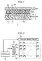
- Fig. 1 is a view showing the section of an electrophoresis device according to the invention.
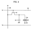
- Fig. 2 is a view schematically illustrating the circuit configuration of an electrophoresis display device.
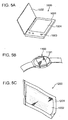
- Fig. 3 is a view illustrating the configuration of each pixel driving circuit.
- Fig. 4A is a view schematically illustrating voltages applied to a pixel electrode and a transparent electrode of the electrophoresis display device
- Fig. 4B is a view showing the relationship of respective voltages shown in Fig. 4A.
- Figs. 5A to 5C are views illustrating concrete examples of electronic apparatuses to which the electrophoresis device of the invention is applied.
- Fig. 1 is a view showing the section of an electrophoresis display device 1 that is an example of the electrophoresis device according to the invention.
- the electrophoresis display device 1 is roughly composed of a first substrate 10, an electrophoretic layer 20, and a second substrate 30.
- a thin film semiconductor circuitry layer 12 is formed on a flexible substrate 11 as an insulating underlying substrate which forms an electric circuit.
- the thickness of the first substrate 10, for example, is desirably 25 ⁇ m or more from the viewpoint of the physical strength of the substrate in forming a thin film circuit, and it is desirably 200 ⁇ m or less from the viewpoint of flexibility of the substrate.
- the flexible substrate 11 is, for example, a polycarbonate substrate having a film thickness of 200 ⁇ m.
- a semiconductor circuit layer 12 is laminated (bonded) via an adhesive layer 11a made of, for example, a UV (ultraviolet rays) curable adhesive.
- resin materials having excellent properties, such as light weight, flexibility, elasticity, etc. can be used.
- the thin film semiconductor circuitry layer 12 includes, for example, a plurality of wiring groups which are arranged in a row direction and in a column direction, respectively, a pixel electrode group, a pixel driving circuit, connecting terminals, and a row decoder 51 and a column decoder (not shown), which select driving pixels, etc.
- the pixel driving circuit includes circuit elements, such as thin-film transistors (TFTs).
- the pixel electrode group contains a plurality of pixel electrodes 13a arranged in a matrix, and forms an image (two-dimensional information) display region.
- An active matrix circuit is formed so that an individual voltage can be applied to each pixel electrodes 13a.
- connection electrode 14 is formed at the peripheral portion of the thin film semiconductor circuitry layer 12 to electrically connect a transparent electrode layer 32 of the second substrate 30 to circuit wiring of the first substrate 10.
- the electrophoretic layer 20 is formed on the pixel electrodes 13a and over their periphery region.
- the electrophoretic layer 20 includes a large number of microcapsules 21 fixed with a binder 22.
- An electrophoretic dispersion medium and electrophoretic particles are contained in the microcapsules 21.
- the electrophoretic particles have a property of moving in the electrophoretic dispersion medium according to an applied voltage, and one or more types of the electrophoretic particles are used.
- the thickness of the electrophoretic layer 20 is, for example, about 30 ⁇ m to 75 ⁇ m.
- the electrophoretic layer 20 can be formed by mixing the above-mentioned microcapsules 21 along with a desired dielectric constant moderator in the binder 22, and coating the resulting resin composition (emulsion or organic solvent solution) on a base material by using known coating methods, such as a method using a roll coater, a method using a roll laminator, a screen printing method, and a spray method. Moreover, in order to surely bring the microcapsules 21 into close contact with the pixel electrodes 13a, an adhesive may be included in the electrophoretic layer 20.
- the electrophoretic dispersion medium a single one of or a mixture of the following materials to which a surfactant and so on is added may be used: water; alcohol solvents such as methanol, ethanol, isopropanol, butanol, octanol and methyl cellosolve; esters such as ethyl acetate and butyl acetate; ketones such as acetone, methyl ethyl ketone and methyl isobutyl ketone; aliphatic hydrocarbons such as pentane, hexane and octane; alicyclic hydrocarbons such as cyclohexane and methylcyclohexane; aromatic hydrocarbons such as benzene, toluene, xylene, hexylbenzene; halogenated hydrocarbons such as methylene chloride, chloroform, carbon tetrachloride and 1,2-dichloroethane; carb
- the electrophoretic particles are particles (polymers or colloids) having the property of moving toward a desired electrode based on electrophoresis by a potential difference in the electrophoretic dispersion medium.
- the electrophoretic particles for example, there are black pigments such as aniline black and carbon black; white pigments such as titanium dioxide, zinc oxide and antimony trioxide; azo-based pigments such as monoazo, dis-azo, and polyazo; yellow pigments such as isoindolenone, chrome yellow, yellow iron oxide, cadmium yellow, titanium yellow, and antimony; red pigments such as quinacrilidone red and chrome vermillion; anthraquinone-based dyes such as phthalocyanine blue and indanthrene blue; blue pigments such as prussian blue and ultramarine blue, cobalt blue, etc.; and green pigments such as phthalocyanine green.
- One of or a plurality of the above types of pigment particles may be used.
- the following agents can be added to these pigments: a charge controlling agent made of particles of an electrolyte, surfactant, metal soap, resin, rubber, oil, varnish, compound or the like; a dispersing agent such as a titanium coupling agent; a lubricating agent; a stabilizing agent; and so forth.
- microcapsules 21 materials having flexibility, such as Arabic-gum/gelatin-based compounds and urethane-based compounds are preferably used.
- the microcapsules 21 can be formed using known microencapsulation techniques, such as an interfacial polymerization method, an insolubilization reaction method, a phase separation method or an interfacial sedimentation method. Further, the microcapsules 21 whose sizes are substantially uniform are preferable since they allow an excellent display function to be exhibited.
- the microcapsules 21 whose sizes are substantially uniform can be obtained by using, for example, filtration or specific gravity difference classification.
- the size of the microcapsules is generally about 30 to 60 ⁇ m.
- the binder 22 is not particularly limited so long as it has a good affinity to the microcapsules 21, an excellent adhesiveness to the electrodes, and insulation property.
- the second substrate 30 is made of a thin film (transparent insulating synthetic resin base material) 31 having the transparent electrode layer (common electrode) 32 formed on the bottom face thereof, and is formed so as to cover the top of the electrophoretic layer 20.
- the thickness of the first substrate 30 is desirably 10 to 200 ⁇ m, and more preferably 25 to 75 ⁇ m.
- a thin film 31 seals and protects the electrophoretic layer 20, and is formed using, for example, a polyethylene terephthalate (PET) film. Similar to the above-described flexible substrate 11, various materials can be used as the thin film 31 if only they are insulating transparent materials. It is favorable that the thickness of the thin film 31 is not more than the thickness of the flexible substrate 11. More preferably, the thickness of the thin film is about half or less the thickness of the flexible substrate 11.
- PET polyethylene terephthalate
- the transparent electrode layer 32 is formed using, for example, a transparent conductive film, such as indium oxide film (ITO film) doped with tin.
- ITO film indium oxide film
- the circuit wiring of the first substrate 10 and the transparent electrode layer 32 of the second substrate 30 are connected on the outside of a region where the electrophoretic layer 20 is formed.
- the transparent electrode layer 32 and the connection electrode 14 of the thin film semiconductor circuitry layer 12 are connected to each other via a conductive connector 23.
- the transparent conductive film constituting the transparent electrode layer 32 for example, a tin oxide film doped with fluorine (FTO film), a zinc oxide film doped with antimony, a zinc oxide film doped with indium, a zinc oxide film doped with aluminum, etc. can be exemplified, in addition to the above-described ITO film.
- FTO film fluorine
- the method of forming the transparent electrode layer 32 on the thin film 31 is not particularly limited, for example, a sputtering method, an electron beam method, an ion-plating method, a vacuum evaporation method, or a chemical vapor deposition (CVD) method can be employed.
- Fig. 2 is a view schematically illustrating the circuit configuration of the electrophoresis display device 1.
- a controller (voltage control means) 52 generates image signals showing an image to be displayed in an image display region 55, reset data for performing reset at the time of image rewriting, and other various signals (clock signals, etc.), and outputs them to a scanning line driving circuit 53 or a data line driving circuit 54.
- the display region 55 is provided with a plurality of data lines (voltage supply means) arranged parallel to the X-direction, a plurality of scanning lines arranged parallel to the Y-direction, and pixel driving circuits disposed at respective intersections of these data lines and scanning lines.
- data lines voltage supply means
- scanning lines arranged parallel to the Y-direction
- pixel driving circuits disposed at respective intersections of these data lines and scanning lines.
- Fig. 3 is a view illustrating the configuration of each pixel driving circuit.
- the gate of a transistor 61 is connected to a scanning line 64, the source thereof is connected to a data line 65, and the drain thereof is connected to the pixel electrode 13a.
- a storage capacitor 63 is connected in parallel with an electrophoretic element.
- the data line 65 supplies a voltage to the pixel electrode 13a and the transparent electrode layer 32 included in each pixel driving circuit, it makes electrophoretic particles of the electrophoretic layer 20 migrate, performing image display.
- the scanning line driving circuit 53 is connected to each scanning line of the display region 55 to select any one of the scanning lines and supply a predetermined scanning line signal Y1, Y2, ⁇ , or Ym to the selected scanning line.
- the scanning line signal Y1, Y2, ⁇ , or Ym is a signal that an active period (H level period) shifts sequentially and this signal is output to each scanning line so that a pixel driving circuit connected to each scanning line may be turned on sequentially.
- the data line driving circuit 54 is connected to each data line of the display region 55 to supply a data signal X1, X2, ⁇ , or Xn to each pixel driving circuit selected by the scanning line driving circuit 53.
- Fig. 4A is a view schematically showing voltages to be applied to the pixel electrode 13a of the electrophoresis display device 1 and the transparent electrode layer 32 via the data line 65 from the controller 52.
- V1 and V2 are supplied to pixel electrodes 13a-1 and 13a-2, respectively, via the data line 65 from the controller 52.
- a voltage drop by wiring resistance along the lines, voltage fluctuation by leak, etc. cause the voltages which actually appears in the pixel electrodes 13a-1 and 13a-2 to shift from V1 and V2 to V3 and V4, respectively.
- the controller 52 applies binary pulse voltages of potentials V5 and V6 to the transparent electrode layer 32.
- a means to apply a voltage to a pixel electrode, and a means to apply a voltage to a common electrode may be separate.
- V5 and V6 are determined in consideration of the wiring resistance on the side of the pixel electrode 13a etc. so that they may be set to V5 ⁇ V3 and V6 ⁇ V4, respectively. Specifically, before the electrophoretic layer 20 is formed, i.e., while the pixel electrode 13a is exposed, V1 and V2 may be applied to the pixel electrode 13a, and the potentials V3 and V4 which actually appear in the pixel electrode 13a at this time may be measured. Otherwise, V3 and V4 may be calculated using the wiring resistance and wiring capacity which are required for the sheet resistivity, length, width, thickness, etc of a wiring pattern.
- the relationship V6 > V3 is satisfied in the region of the pixel electrode 13a-1 of the potential V3. Therefore, an electric field is generated in the direction of the pixel electrode 13a, and if electrophoretic particles are charged positively, the electrophoretic particles migrate toward the direction of the pixel electrode 13a-1.
- the relationship V6 ⁇ V4 is satisfied in the region of the pixel electrode 13a-2 of the potential V4, an electric field is not generated, or even if an electric field is generated, it is generated in the direction of the transparent electrode layer 32. Therefore, electrophoretic particles migrate toward the direction of the transparent electrode layer 32.
- the relationship V4 > V5 is satisfied in the region of the pixel electrode 13a-2 of the potential V4. Therefore, an electric field is generated in the direction of the transparent electrode layer 32, and electrophoretic particles which are charged positively migrate toward the direction of the transparent electrode layer 32.
- the relationship V5 ⁇ V3 is satisfied in the region of the pixel electrode 13a-1 of the potential V3, an electric field is not generated, or even if an electric field is generated, it is generated in the direction of the pixel electrode. Therefore, electrophoretic particles migrate toward the direction of the pixel electrode 13a-1.
- electrophoretic particles are prevented from migrating in a direction reverse to a desired direction.
- the substantial duty ratio of a pulse voltage applied to the transparent electrode layer 32 is desirably 50%. This allows uniform application of bipolarity, which makes it possible to prevent deterioration of display unevenness and dispersion liquid.
- the period of pulses applied to a common electrode is desirably 50 to 1000 ms. If the period is less than 50 ms, electrophoretic particles cannot response satisfactorily. If the period is not less than 1000 ms, display switching time may become too long.
- V3 is slightly higher than V1
- V4 is slightly lower than V2
- the invention is not limited thereto. That is, the object of the invention can be achieved if V5 and V6 are set to be V5 ⁇ V3 and V6 ⁇ V4, respectively, regardless of the hierarchical relation of V1 and V3, and V4 and V2.
- the electrophoretic layer 20 of the electrophoresis display device 1 includes a plurality of microcapsules 21, even if the electrophoretic layer 20 does not include the microcapsules 21, it needs only to be a layer formed of an electrophoretic dispersion liquid containing electrophoretic particles.
- the pixel electrode group is arranged in a matrix to form the active matrix circuit, arrangement of the pixel electrode group is not limited thereto.
- Fig. 5 is a perspective view illustrating concrete examples of electronic apparatuses to which the electrophoresis device of the invention is applied.
- Fig. 5A is a perspective view showing an electronic book that is an example of an electronic apparatus.
- This electronic book 1000 includes a book-shaped frame 1001, an (openable and closable) cover 1002 rotatably provided with respect to the frame 1001, an operation unit 1003, and a display unit 1004 composed of the electrophoresis device according to the present embodiment.
- Fig. 5B is a perspective view showing a wrist watch that is an example of an electronic apparatus.
- This wrist watch 1100 includes a display unit 1101 composed of the electrophoresis device according to the present embodiment.
- Fig. 5C is a perspective view showing an electronic paper that is an example of an electronic apparatus.
- This electronic paper 1200 is made of rewritable sheets having the same texture and flexibility as paper.
- the electronic paper includes a main body 1201, and a display unit 1202 composed of the electrophoresis device according to the present embodiment.
- the electronic apparatuses to which the electrophoresis device can be applied are not limited thereto, but widely include apparatuses utilizing changes in a visual tone accompanying migration of charged particles.
- the electronic apparatuses also involves things belonging to real estate, such as wall surfaces to which an electrophoretic film is bonded, and things belonging to movable bodies, such vehicles, flying bodies, and vessels, in addition to the apparatuses as described above.
Landscapes
- Engineering & Computer Science (AREA)
- Physics & Mathematics (AREA)
- Computer Hardware Design (AREA)
- General Physics & Mathematics (AREA)
- Theoretical Computer Science (AREA)
- Electrochromic Elements, Electrophoresis, Or Variable Reflection Or Absorption Elements (AREA)
Applications Claiming Priority (1)
| Application Number | Priority Date | Filing Date | Title |
|---|---|---|---|
| JP2005276543A JP4530167B2 (ja) | 2005-09-22 | 2005-09-22 | 電気泳動装置、電子機器、および電気泳動装置の駆動方法 |
Publications (2)
| Publication Number | Publication Date |
|---|---|
| EP1775709A2 true EP1775709A2 (de) | 2007-04-18 |
| EP1775709A3 EP1775709A3 (de) | 2010-11-24 |
Family
ID=37461432
Family Applications (1)
| Application Number | Title | Priority Date | Filing Date |
|---|---|---|---|
| EP06019571A Withdrawn EP1775709A3 (de) | 2005-09-22 | 2006-09-19 | Elektroforesevorrichtung, elektronisches Gerät und Ansteuerverfahren für eine Elektroforesevorrichtung |
Country Status (4)
| Country | Link |
|---|---|
| US (1) | US8089452B2 (de) |
| EP (1) | EP1775709A3 (de) |
| JP (1) | JP4530167B2 (de) |
| CN (1) | CN100523977C (de) |
Families Citing this family (18)
| Publication number | Priority date | Publication date | Assignee | Title |
|---|---|---|---|---|
| JP5125378B2 (ja) | 2007-10-03 | 2013-01-23 | セイコーエプソン株式会社 | 制御方法、制御装置、表示体および情報表示装置 |
| CN101878393B (zh) * | 2007-11-29 | 2012-04-04 | 夏普株式会社 | 光源装置和具备它的显示装置 |
| JP2009175492A (ja) | 2008-01-25 | 2009-08-06 | Seiko Epson Corp | 電気泳動表示装置及びその駆動方法並びに電子機器 |
| US8310423B2 (en) * | 2008-03-05 | 2012-11-13 | Epson Imaging Devices Corporation | Liquid crystal display device and head-up display |
| US8437069B2 (en) * | 2008-03-11 | 2013-05-07 | Sipix Imaging, Inc. | Luminance enhancement structure for reflective display devices |
| CN101971073A (zh) * | 2008-03-11 | 2011-02-09 | 矽峰成像股份有限公司 | 用于反射型显示器的辉度增强结构 |
| US8441414B2 (en) | 2008-12-05 | 2013-05-14 | Sipix Imaging, Inc. | Luminance enhancement structure with Moiré reducing design |
| US20100177396A1 (en) * | 2009-01-13 | 2010-07-15 | Craig Lin | Asymmetrical luminance enhancement structure for reflective display devices |
| US9025234B2 (en) * | 2009-01-22 | 2015-05-05 | E Ink California, Llc | Luminance enhancement structure with varying pitches |
| US8714780B2 (en) * | 2009-04-22 | 2014-05-06 | Sipix Imaging, Inc. | Display devices with grooved luminance enhancement film |
| US8797633B1 (en) | 2009-07-23 | 2014-08-05 | Sipix Imaging, Inc. | Display device assembly and manufacture thereof |
| US8456589B1 (en) | 2009-07-27 | 2013-06-04 | Sipix Imaging, Inc. | Display device assembly |
| US20140062849A1 (en) * | 2012-09-05 | 2014-03-06 | Tagnetics, Inc. | Cmos-compatible display system and method |
| CA3002202A1 (en) | 2017-04-25 | 2018-10-25 | Emil J. Gulbranson | Hay bale dryer |
| EP3631575A4 (de) * | 2017-05-30 | 2021-01-13 | E Ink Corporation | Elektro-optische anzeigen |
| US11404013B2 (en) | 2017-05-30 | 2022-08-02 | E Ink Corporation | Electro-optic displays with resistors for discharging remnant charges |
| CN110070835B (zh) * | 2018-01-22 | 2021-05-28 | 矽创电子股份有限公司 | 电子纸显示驱动电路 |
| CN109830217B (zh) * | 2019-04-09 | 2021-04-09 | 上海中航光电子有限公司 | 液晶显示面板、显示装置和驱动方法 |
Family Cites Families (13)
| Publication number | Priority date | Publication date | Assignee | Title |
|---|---|---|---|---|
| JPS5922947B2 (ja) | 1975-10-20 | 1984-05-30 | 松下電器産業株式会社 | 電気泳動表示パネルの駆動方式 |
| KR950001360B1 (ko) * | 1990-11-26 | 1995-02-17 | 가부시키가이샤 한도오따이 에네루기 겐큐쇼 | 전기 광학장치와 그 구동방법 |
| US5392058A (en) * | 1991-05-15 | 1995-02-21 | Sharp Kabushiki Kaisha | Display-integrated type tablet device |
| JP4491854B2 (ja) * | 1999-05-14 | 2010-06-30 | ブラザー工業株式会社 | 電気泳動表示装置 |
| JP2002075064A (ja) * | 2000-08-23 | 2002-03-15 | Tdk Corp | 異方導電性フィルム及びその製造方法並びに異方導電性フィルムを用いた表示装置 |
| US6724521B2 (en) * | 2001-03-21 | 2004-04-20 | Kabushiki Kaisha Toshiba | Electrophoresis display device |
| JP2003197994A (ja) * | 2001-08-31 | 2003-07-11 | Ngk Insulators Ltd | 圧電/電歪アクチュエータの変位劣化の補償方法 |
| CN102789764B (zh) | 2001-11-20 | 2015-05-27 | 伊英克公司 | 驱动双稳态电光显示器的方法 |
| US7259745B2 (en) * | 2003-03-05 | 2007-08-21 | Canon Kabushiki Kaisha | Method for driving electrophoresis display apparatus |
| JP2004325489A (ja) * | 2003-04-21 | 2004-11-18 | Canon Inc | 電気泳動表示装置 |
| EP1656658A4 (de) * | 2003-08-19 | 2009-12-30 | E Ink Corp | Verfahren zur steuerung von elektrooptischen displays |
| JP4287310B2 (ja) * | 2004-03-10 | 2009-07-01 | 株式会社東芝 | 電気泳動表示素子の駆動方法 |
| JP4718859B2 (ja) * | 2005-02-17 | 2011-07-06 | セイコーエプソン株式会社 | 電気泳動装置とその駆動方法、及び電子機器 |
-
2005
- 2005-09-22 JP JP2005276543A patent/JP4530167B2/ja not_active Expired - Lifetime
-
2006
- 2006-08-28 US US11/467,647 patent/US8089452B2/en active Active
- 2006-09-18 CN CNB2006101534745A patent/CN100523977C/zh active Active
- 2006-09-19 EP EP06019571A patent/EP1775709A3/de not_active Withdrawn
Also Published As
| Publication number | Publication date |
|---|---|
| JP4530167B2 (ja) | 2010-08-25 |
| JP2007086529A (ja) | 2007-04-05 |
| CN100523977C (zh) | 2009-08-05 |
| CN1936683A (zh) | 2007-03-28 |
| EP1775709A3 (de) | 2010-11-24 |
| US8089452B2 (en) | 2012-01-03 |
| US20070063965A1 (en) | 2007-03-22 |
Similar Documents
| Publication | Publication Date | Title |
|---|---|---|
| US8089452B2 (en) | Electrophoresis device, electronic apparatus, and driving method of electrophoresis device | |
| US12253784B2 (en) | Electro-optic displays and driving methods | |
| KR100437329B1 (ko) | 전기 영동 장치, 전기 영동 장치의 구동 방법, 전기 영동장치의 구동 회로, 및 전자기기 | |
| US6531997B1 (en) | Methods for addressing electrophoretic displays | |
| US11735127B2 (en) | Electro-optic displays and driving methods | |
| US11450287B2 (en) | Electro-optic displays | |
| KR20070095790A (ko) | 전기 영동 장치, 전자 기기, 및 전기 영동 장치의 구동방법 | |
| EP3414613B1 (de) | Verfahren und vorrichtung zum betrieb einer elektrooptischen anzeige im weissmodus | |
| JP2005148711A (ja) | 表示装置、表示装置の駆動方法および電子機器 | |
| US11521565B2 (en) | Crosstalk reduction for electro-optic displays | |
| US12249262B2 (en) | Methods for measuring electrical properties of electro-optic displays | |
| JP4659417B2 (ja) | 電気泳動表示装置 | |
| CN118435269A (zh) | 用于驱动电光显示器的方法 | |
| JP2007078843A (ja) | 電気泳動装置、電子機器、および電気泳動装置の駆動方法 | |
| CN121909419A (zh) | 具有共享透明电极的反射式显示器与投射电容式触摸传感器 | |
| HK40048029A (en) | Electro-optic displays |
Legal Events
| Date | Code | Title | Description |
|---|---|---|---|
| PUAI | Public reference made under article 153(3) epc to a published international application that has entered the european phase |
Free format text: ORIGINAL CODE: 0009012 |
|
| AK | Designated contracting states |
Kind code of ref document: A2 Designated state(s): AT BE BG CH CY CZ DE DK EE ES FI FR GB GR HU IE IS IT LI LT LU LV MC NL PL PT RO SE SI SK TR |
|
| AX | Request for extension of the european patent |
Extension state: AL BA HR MK YU |
|
| PUAL | Search report despatched |
Free format text: ORIGINAL CODE: 0009013 |
|
| AK | Designated contracting states |
Kind code of ref document: A3 Designated state(s): AT BE BG CH CY CZ DE DK EE ES FI FR GB GR HU IE IS IT LI LT LU LV MC NL PL PT RO SE SI SK TR |
|
| AX | Request for extension of the european patent |
Extension state: AL BA HR MK RS |
|
| 17P | Request for examination filed |
Effective date: 20110510 |
|
| AKX | Designation fees paid |
Designated state(s): DE FR GB |
|
| 17Q | First examination report despatched |
Effective date: 20110823 |
|
| STAA | Information on the status of an ep patent application or granted ep patent |
Free format text: STATUS: THE APPLICATION HAS BEEN WITHDRAWN |
|
| 18W | Application withdrawn |
Effective date: 20150811 |