EP1777530A9 - Verfahren und Vorrichtung zur Strommessungen an Wechselrichterausgängen - Google Patents
Verfahren und Vorrichtung zur Strommessungen an Wechselrichterausgängen Download PDFInfo
- Publication number
- EP1777530A9 EP1777530A9 EP05109738A EP05109738A EP1777530A9 EP 1777530 A9 EP1777530 A9 EP 1777530A9 EP 05109738 A EP05109738 A EP 05109738A EP 05109738 A EP05109738 A EP 05109738A EP 1777530 A9 EP1777530 A9 EP 1777530A9
- Authority
- EP
- European Patent Office
- Prior art keywords
- current
- inverter
- voltage
- output phase
- measured
- Prior art date
- Legal status (The legal status is an assumption and is not a legal conclusion. Google has not performed a legal analysis and makes no representation as to the accuracy of the status listed.)
- Granted
Links
- 238000000034 method Methods 0.000 title claims abstract description 34
- 238000005259 measurement Methods 0.000 claims abstract description 63
- 230000015572 biosynthetic process Effects 0.000 claims description 2
- 238000001914 filtration Methods 0.000 claims 1
- 238000005070 sampling Methods 0.000 description 9
- 230000006870 function Effects 0.000 description 7
- 230000010355 oscillation Effects 0.000 description 7
- 230000000694 effects Effects 0.000 description 5
- 230000001052 transient effect Effects 0.000 description 3
- 238000004364 calculation method Methods 0.000 description 2
- 230000001419 dependent effect Effects 0.000 description 2
- ZYHIULSBMGTPBF-UHFFFAOYSA-N 1-(3-aminopropyl)-3-(2,6-dimethylphenyl)urea Chemical compound Cc1cccc(C)c1NC(=O)NCCCN ZYHIULSBMGTPBF-UHFFFAOYSA-N 0.000 description 1
- 230000006399 behavior Effects 0.000 description 1
- 230000003247 decreasing effect Effects 0.000 description 1
- 238000000691 measurement method Methods 0.000 description 1
- 238000001208 nuclear magnetic resonance pulse sequence Methods 0.000 description 1
- 239000004065 semiconductor Substances 0.000 description 1
- LXMSZDCAJNLERA-ZHYRCANASA-N spironolactone Chemical compound C([C@@H]1[C@]2(C)CC[C@@H]3[C@@]4(C)CCC(=O)C=C4C[C@H]([C@@H]13)SC(=O)C)C[C@@]21CCC(=O)O1 LXMSZDCAJNLERA-ZHYRCANASA-N 0.000 description 1
Images


Classifications
-
- G—PHYSICS
- G01—MEASURING; TESTING
- G01R—MEASURING ELECTRIC VARIABLES; MEASURING MAGNETIC VARIABLES
- G01R19/00—Arrangements for measuring currents or voltages or for indicating presence or sign thereof
- G01R19/25—Arrangements for measuring currents or voltages or for indicating presence or sign thereof using digital measurement techniques
- G01R19/2513—Arrangements for monitoring electric power systems, e.g. power lines or loads; Logging
-
- G—PHYSICS
- G01—MEASURING; TESTING
- G01R—MEASURING ELECTRIC VARIABLES; MEASURING MAGNETIC VARIABLES
- G01R35/00—Testing or calibrating of apparatus covered by the other groups of this subclass
- G01R35/005—Calibrating; Standards or reference devices, e.g. voltage or resistance standards, "golden" references
-
- G—PHYSICS
- G01—MEASURING; TESTING
- G01R—MEASURING ELECTRIC VARIABLES; MEASURING MAGNETIC VARIABLES
- G01R31/00—Arrangements for testing electric properties; Arrangements for locating electric faults; Arrangements for electrical testing characterised by what is being tested not provided for elsewhere
- G01R31/40—Testing power supplies
Definitions
- the present invention relates to a method and arrangement for measuring inverter output phase currents, and more particularly to a method in which phase currents are measured using measurement in a DC-voltage intermediate circuit.
- Voltage source inverters are commonly used for controlling electrical loads such as motors or generators with controllable frequency. Voltage source inverters have a direct current intermediate circuit, through which energy is transferred as a DC voltage to the output switches of the inverter, which further generate DC voltage pulses to the load.
- These voltage pulses are stepwise voltage changes which are known to generate a capacitive charge and discharge currents. Cables that are connected from the output of an inverter to the load are somewhat capacitive against the earth and against the cables of other phases, and this capacitance is charged when the output voltage of the inverter changes abruptly.
- each phase current is measured separately, the above problem are avoided by timing the measurement such that the effects of the stray current are decreased. This can be carried out for example by measuring the current at a specific instant which is long after the previous change of the inverter output state.
- the output current can be measured in an intermediate voltage circuit. All current outputted from an inverter is flown through the intermediate circuit. By measuring the current of the plus or minus voltage bus and by knowing the state of the output switches at the time of a current sample, it is possible to know to which phase the measured current flows. It is thus possible to reconstruct the phase currents one at a time from the output switch positions and current samples. In this measurement method, only one current transducer is needed for making DC current measurement cost effective and simple. Further, the use of DC current measurement requires little space since only one current transducer is needed. These advantages make the DC-current measurement an attractive choice.
- DC current measurement current measurement is carried out when an active voltage vector, i.e. not a zero vector, is chosen since a DC bus carries no current when a zero vector is selected.
- Modulation schemes can be selected such that an active voltage vector enabling a current measurement is chosen at a predetermined time instant. This time instant in relation to a modulation period is usually at the beginning or in the middle of each period.
- An object of the present invention is thus to provide a method and an arrangement for implementing the method so as to overcome the above problem in measuring a DC current of an intermediate voltage circuit and to obtain reliable phase current information representing the current of a load.
- the object of the invention is achieved by a method and an arrangement which are characterized by what is stated in the independent claims. Preferred embodiments of the invention are disclosed in the dependent claims.
- the invention is based on the idea of measuring, at precise intervals, charge and discharge currents before actual use of the inverter. This measured information is then used during the use of the inverter to obtain as accurate load current values as possible.
- An advantage of the method of the invention is that the load current can be determined more accurately using DC-current measurement. If the load is an electrical motor, the whole control of the drive is usually dependent on the accuracy of the load current values.
- a stator current is also used in estimations of motor parameters, as an input to motor models depicting the electrical state of the motor, and in other control related processes calculated in the processors of control equipment of a frequency converter.
- the first steps are taken during commissioning of an inverter in question i.e. before actual use of the inverter.
- a drive is put to use by starting an identification procedure. Identification procedures are commonly used before the first start where a frequency converter executes a procedure where it measures different values, generates parameters for the control, etc.
- a voltage source inverter forms consecutive voltage pulses to the load. These voltage pulses are preferably identical to each other and generated with the same phase. After each pulse, a current sample is taken. The measurement instant of the current measurement is changed in respect to each voltage pulse, and only one current sample is taken during each voltage pulse. The measurement instant is changed in small steps, so that sample data represent the current as well as possible.
- the frequency of capacitive oscillation is typically in the range of 100 kHz to 1 MHz, depending on the type and length of the cabling. This means that minimum sampling frequency should be at least 2 MHz so that sample data can be gathered without aliasing of the data.
- Current transducers achieving these kinds of frequencies are costly, and during normal use of the inverter the gain achieved with them would be minimal.
- sampling of the current by shifting the sampling instant with respect to the start of the voltage pulse is a more cost effective solution giving same results during the operation of the inverter. If, for example, a sampling rate is selected to be 18,75 MHz, the resolution of the current samples becomes 53 ns. Thus the timing of measurement is changed 53 ns for each voltage pulse.
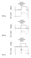
- Figure 2 shows one possible way of sampling the current.
- the first voltage pulse is generated in Figure 2a, and the DC-current is measured time period ts after the voltage pulse.
- Time period ts corresponds to the time resolution of the measurement.
- Figure 2b it can be seen that the voltage pulse is generated earlier in the modulation period than in Figure 2a, but the measurement is carried out at the same instant in the modulation period. Thus, the time difference between the start of the voltage pulse and the measurement is changed.
- Figure 2c the voltage pulse is generated further earlier by ts, and the third current sample is measured.
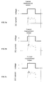
- Figure 3 shows an alternative way of sampling the current.
- the voltage pulse is kept similar and timely in the same place from period to period, but the measurement instant is changed from each previous pulse by ts.
- the consecutive pulses are formed from pulses represented in plots a, b and c.
- the total current flowing from the inverter part of the frequency converter is gained.
- the value of the DC current caused by the consecutive voltage pulses is removed from the measured current samples to obtain sample values for stray current.
- the removal of the DC current can be carried out by estimating the load current and subtracting the load current from the samples.
- the load current can be estimated by dividing the average voltage caused by the consecutive voltage pulses by the load resistance. If the load is an electrical motor, the load resistance is the stator resistance, which is also a typical quantity estimated during an identification run.
- the average voltage caused by the voltage pulses is easy to calculate, since the pulse sequence is determined beforehand.
- ripple currents that are fed to the load are large, they can also be taken into account in the calculation of the stray currents.
- the remaining current is the sample data of the capacitive stray current.
- Another possibility of removing the DC-current component from the sample data is to high-pass filter the data.
- the high-pass filter only leaves the highest frequency components to remain and thus blocks the DC-current and even the ripple current from the sample data.
- stray currents are stored together with their time instants with respect to the start of the respective voltage pulses, and the formation of the voltage pulses is stopped. It should be noted that if a function, rather than samples, is formed, the parametres of that function are stored in the memory of the device. It should also be noted that it is possible to subtract the load current and ripple current from the measured samples immediately after the sample is taken, if the values of load current and ripple current are known.
- Voltage pulses are formed as long as necessary for obtaining a representative sample, or so that oscillation is decayed to a level unnecessary to take into account.
- DC-currents can be measured for various different switching situations. Measurements can be carried out for example for each output phase separately or for different usual modulation patterns.
- the sample data representing the capacitive stray currents After the sample data representing the capacitive stray currents have been stored, the sample data is ready to be put to use.
- DC bus current is measured and the output phase current is determined from the measured current and from the stored data.
- the stored data can be used in different ways.
- the DC current measurement is carried out in a normal way, which means that DC current is measured at a specific instant in a modulation period. This instant can be for example at the end or beginning of the modulation period or in the middle of the modulation period.
- the effects of capacitive currents are then removed from the measured DC current to achieve output phase current that represents the real current flowing to the load.
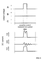
- the removal of the capacitive currents can simply be carried out by calculating the time from the output voltage change to the measurement instant, and subtracting a stored data sample which was taken at a corresponding instant. This is shown in Figure 7, where the upper plot is the voltage pulse, the middle plot is the DC current, and the lower plot shows the stored sample data as separate samples in time domain.
- the sample corresponding to the time period between the switching and the DC current measurement which is shown in the middle plot as a two-ended arrow, is subtracted from the measured DC-current. This subtraction gives the value of the load current.
- Another possibility to take the sample data into account is to carry out the measurement at a time instant at which the capacitive current is known to have a zero crossing point.
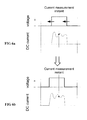
- This variation may utilize of the stored information on the frequency of the oscillation. This can be carried out either by changing the DC current measurement instant as shown in Figures 5a and 5b, or by changing the starting time of the voltage pulse, as shown in Figures 6a and 6b.
- the voltage pulse is shown in the upper plot and the DC current is shown in the lower plot.
- a normal measurement instant is shown to be in the middle of the modulation period.
- the DC current measured at a normal measurement time comprises an error due to the capacitive current.
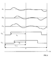
- the capacitive current seen in the DC-current is affected by all inverter output state changes during the modulation period in which the DC-current is measured. This means that the changes of all inverter phases have to be taken into account in the stray currents.
- the measured data samples are stored in a memory as an array that can be indexed using time. As explained above, the samples are stored in connection with the time from the voltage change.
- DIR A , DIR B and DIR C are the direction of change of phases A, B and C, which may obtain a value 1 or -1
- function f(t) represents the stray current values stored, which obtain a value depending on the time between an output state change and the DC-current measurement instant.
- the first output state change occurs at time instant t meas - t A , t meas , which is a half of the modulation period T.
- the output of phase A is switched from a negative intermediate circuit voltage to the positive voltage. This voltage change accomplishes stray current ⁇ i A , which is shown in Figure 4.
- phase B is also controlled to a positive state, and this change also causes capacitive stray currents ⁇ i B to flow. Both of these state changes are from negative potential to positive potential, so both the DIR functions obtain a value 1 in the above equation.
- Time values from the state change to current measurement t A , t B and t C for a three-phase system can be calculated fast if the DC-current measurement is at a predetermined position inside the modulation period. If the DC-current measurement takes place in the middle of the modulation period, as in the above example, the time values are a half of the on-time of the corresponding output switch. The on-time for all the output switches is usually known at the beginning of each modulation period.
- sample data are stored as function parameters, it is still possible to combine these functions for different phases and calculate a time instant at which the capacitive current has a zero crossing point and carry out the measurement of DC-current at this time instant.
- This combination of functions is, however, much more time consuming than the pure use of look-up tables.
- the current value can be approximated to be the nearest one, or a linear interpolation may be used between the nearest stored current values to obtain a better approximation.
- the method of the present invention can be carried out by means of a processor used in any modern frequency converter.
- processors have a high clock frequency, enabling the current measurement time or the position and duration of the voltage pulse in a modulation period to be set precisely.
- the method further necessitates a means for storing the collected measurement data, such as a semiconductor memory, and a link between the processor and the memory.
- the processor can thus store values into storing means and read values from the storing means.
- the processor can also be programmed to execute the required calculations.
Landscapes
- Physics & Mathematics (AREA)
- General Physics & Mathematics (AREA)
- Engineering & Computer Science (AREA)
- Power Engineering (AREA)
- Inverter Devices (AREA)
- Power Conversion In General (AREA)
Priority Applications (4)
| Application Number | Priority Date | Filing Date | Title |
|---|---|---|---|
| AT05109738T ATE415635T1 (de) | 2005-10-19 | 2005-10-19 | Verfahren und vorrichtung zur strommessung an wechselrichterausgängen |
| EP05109738A EP1777530B1 (de) | 2005-10-19 | 2005-10-19 | Verfahren und Vorrichtung zur Strommessung an Wechselrichterausgängen |
| DE602005011301T DE602005011301D1 (de) | 2005-10-19 | 2005-10-19 | Verfahren und Vorrichtung zur Strommessung an Wechselrichterausgängen |
| US11/540,638 US7508688B2 (en) | 2005-10-19 | 2006-10-02 | Method and arrangement for measuring output phase currents of a voltage source inverter under a load |
Applications Claiming Priority (1)
| Application Number | Priority Date | Filing Date | Title |
|---|---|---|---|
| EP05109738A EP1777530B1 (de) | 2005-10-19 | 2005-10-19 | Verfahren und Vorrichtung zur Strommessung an Wechselrichterausgängen |
Publications (3)
| Publication Number | Publication Date |
|---|---|
| EP1777530A1 EP1777530A1 (de) | 2007-04-25 |
| EP1777530A9 true EP1777530A9 (de) | 2007-08-22 |
| EP1777530B1 EP1777530B1 (de) | 2008-11-26 |
Family
ID=36067263
Family Applications (1)
| Application Number | Title | Priority Date | Filing Date |
|---|---|---|---|
| EP05109738A Expired - Lifetime EP1777530B1 (de) | 2005-10-19 | 2005-10-19 | Verfahren und Vorrichtung zur Strommessung an Wechselrichterausgängen |
Country Status (4)
| Country | Link |
|---|---|
| US (1) | US7508688B2 (de) |
| EP (1) | EP1777530B1 (de) |
| AT (1) | ATE415635T1 (de) |
| DE (1) | DE602005011301D1 (de) |
Families Citing this family (12)
| Publication number | Priority date | Publication date | Assignee | Title |
|---|---|---|---|---|
| ATE547713T1 (de) * | 2008-09-23 | 2012-03-15 | Abb Oy | Strommessung in einem wechselrichter und in einem frequenzwandler |
| DE102009048509A1 (de) * | 2009-10-09 | 2011-04-14 | Abb Technology Ag | Verfahren und Vorrichtung zur Ermittlung einer Eingangsspannung an einer Ortsnetzstation eines Stromnetzes |
| FR2967260B1 (fr) * | 2010-11-09 | 2012-11-16 | Valeo Systemes Thermiques | Mesure de courant pour radiateur electrique |
| CN103116059B (zh) * | 2013-01-21 | 2013-10-16 | 山东大学 | 适用于并网发电系统低电压穿越功能的电压快速检测算法 |
| US10277115B2 (en) | 2016-04-15 | 2019-04-30 | Emerson Climate Technologies, Inc. | Filtering systems and methods for voltage control |
| US10312798B2 (en) | 2016-04-15 | 2019-06-04 | Emerson Electric Co. | Power factor correction circuits and methods including partial power factor correction operation for boost and buck power converters |
| US10763740B2 (en) | 2016-04-15 | 2020-09-01 | Emerson Climate Technologies, Inc. | Switch off time control systems and methods |
| US9933842B2 (en) | 2016-04-15 | 2018-04-03 | Emerson Climate Technologies, Inc. | Microcontroller architecture for power factor correction converter |
| US10656026B2 (en) | 2016-04-15 | 2020-05-19 | Emerson Climate Technologies, Inc. | Temperature sensing circuit for transmitting data across isolation barrier |
| US10284132B2 (en) | 2016-04-15 | 2019-05-07 | Emerson Climate Technologies, Inc. | Driver for high-frequency switching voltage converters |
| US10305373B2 (en) * | 2016-04-15 | 2019-05-28 | Emerson Climate Technologies, Inc. | Input reference signal generation systems and methods |
| US11837964B2 (en) | 2019-04-10 | 2023-12-05 | Danfoss Power Electronics A/S | Method for detecting low impedance condition at output of electrical converter, control unit, computer program product and electrical converter |
Family Cites Families (13)
| Publication number | Priority date | Publication date | Assignee | Title |
|---|---|---|---|---|
| US4213134A (en) * | 1979-02-26 | 1980-07-15 | The University Of Akron | Circuit and method for the recorder display of high frequency periodic signals |
| US4791404A (en) * | 1986-03-03 | 1988-12-13 | Tektronix, Inc. | Predictive time base control circuit for a waveform system |
| JPS63228969A (ja) * | 1987-03-18 | 1988-09-22 | Toshiba Corp | インバ−タ装置の出力電流検出装置 |
| JPH04156292A (ja) * | 1990-10-16 | 1992-05-28 | Toshiba Corp | 永久磁石形電動機の制御装置 |
| JP2809902B2 (ja) * | 1991-09-25 | 1998-10-15 | 株式会社東芝 | 自励式変換器の試験方法 |
| JPH05292753A (ja) * | 1992-04-10 | 1993-11-05 | Meidensha Corp | Pwmインバータの電流検出方法 |
| US5309349A (en) * | 1992-09-22 | 1994-05-03 | Industrial Technology Research Institute | Current detection method for DC to three-phase converters using a single DC sensor |
| DK172570B1 (da) * | 1995-01-23 | 1999-01-25 | Danfoss As | Vekselretter og fremgangsmåde til måling af vekselretterens fasestrømme |
| FR2752111B1 (fr) * | 1996-07-30 | 1998-10-30 | Texas Instruments France | Procede et dispositif de commande d'onduleurs |
| US6735537B2 (en) * | 2002-03-15 | 2004-05-11 | Motorola, Inc. | Procedure for measuring the current in each phase of a three-phase device via single current sensor |
| US20060071627A1 (en) * | 2002-03-28 | 2006-04-06 | Ho Eddy Y Y | Motor current reconstruction via DC bus current measurement |
| JP4055992B2 (ja) * | 2002-12-25 | 2008-03-05 | サンデン株式会社 | インバータの電流検出装置 |
| US7348758B2 (en) * | 2005-10-26 | 2008-03-25 | International Rectifier Corporation | Audible noise reduction for single current shunt platform |
-
2005
- 2005-10-19 DE DE602005011301T patent/DE602005011301D1/de not_active Expired - Lifetime
- 2005-10-19 AT AT05109738T patent/ATE415635T1/de not_active IP Right Cessation
- 2005-10-19 EP EP05109738A patent/EP1777530B1/de not_active Expired - Lifetime
-
2006
- 2006-10-02 US US11/540,638 patent/US7508688B2/en active Active
Also Published As
| Publication number | Publication date |
|---|---|
| US20070085546A1 (en) | 2007-04-19 |
| EP1777530A1 (de) | 2007-04-25 |
| DE602005011301D1 (de) | 2009-01-08 |
| ATE415635T1 (de) | 2008-12-15 |
| US7508688B2 (en) | 2009-03-24 |
| EP1777530B1 (de) | 2008-11-26 |
Similar Documents
| Publication | Publication Date | Title |
|---|---|---|
| JP6407978B2 (ja) | 電気信号計測 | |
| Pu et al. | Fault diagnosis of DC-link capacitors in three-phase AC/DC PWM converters by online estimation of equivalent series resistance | |
| EP1777530B1 (de) | Verfahren und Vorrichtung zur Strommessung an Wechselrichterausgängen | |
| US10132846B2 (en) | Method of and apparatus for learning the phase error or timing delays within a current transducer and power measurement apparatus including current transducer error correction | |
| EP3499676B1 (de) | Stromwandler | |
| JP4298223B2 (ja) | 電源システム | |
| JPS6250764B2 (de) | ||
| US4820973A (en) | Impedance measuring system | |
| EP1863160A2 (de) | Messung des Stroms eines Frequenzumrichters | |
| GB2143958A (en) | Tracking filter for sensing dc content in an ac waveform | |
| EP1729141B1 (de) | Verfahren zur Ermittlung der Rotorzeitkonstanten einer Asynchronmaschine | |
| EP1956380B1 (de) | Verfahren und entsprechende Vorrichtung zur Schätzung zweier gleichzeitig fließender Ströme durch entsprechende Wicklungen einer mit Raumzeigermodulation betriebenen mehrphasigen elektrischen Last | |
| US4546301A (en) | Circuit and method for controlling an alternating or three-phase current motor | |
| HU218529B (hu) | Elrendezés és eljárás villamos teljesítmény mérésére | |
| US6195274B1 (en) | Method for defining instantaneous value of current of pulse-controlled inductive load | |
| EP0573088A1 (de) | Verfahren und Schaltung zur Regelung eines Wechselrichters im Gleitmodus und mit einer PBM geschalteten dreistufigen Ausgangsspannung | |
| EP4597140A1 (de) | Überwachungsmodul und verfahren zur überwachung der leistungsverschlechterung eines kondensators | |
| Schubert et al. | Gate driver integrated instantaneous phase voltage measurement in PWM voltage source inverters | |
| US7262577B2 (en) | Method for estimating the sum of stator and rotor resistances | |
| JP7572204B2 (ja) | リアクトル損失測定装置及び波形測定装置 | |
| JP3625966B2 (ja) | 周波数測定装置 | |
| DE102016222754A1 (de) | Verfahren zum Betreiben eines Frequenzumrichters und Frequenzumrichter | |
| DE102023123276B4 (de) | Verfahren zum Ermitteln von stromabhängigen Induktivitäten einer mehrphasigen elektrischen Maschine und Frequenzumrichter | |
| JPH11326428A (ja) | インバータ回路のパラメータ測定装置 | |
| JP3703925B2 (ja) | 保護継電器の試験装置 |
Legal Events
| Date | Code | Title | Description |
|---|---|---|---|
| PUAI | Public reference made under article 153(3) epc to a published international application that has entered the european phase |
Free format text: ORIGINAL CODE: 0009012 |
|
| AK | Designated contracting states |
Kind code of ref document: A1 Designated state(s): AT BE BG CH CY CZ DE DK EE ES FI FR GB GR HU IE IS IT LI LT LU LV MC NL PL PT RO SE SI SK TR |
|
| AX | Request for extension of the european patent |
Extension state: AL BA HR MK YU |
|
| 17P | Request for examination filed |
Effective date: 20070531 |
|
| AKX | Designation fees paid |
Designated state(s): AT BE BG CH CY CZ DE DK EE ES FI FR GB GR HU IE IS IT LI LT LU LV MC NL PL PT RO SE SI SK TR |
|
| GRAP | Despatch of communication of intention to grant a patent |
Free format text: ORIGINAL CODE: EPIDOSNIGR1 |
|
| GRAS | Grant fee paid |
Free format text: ORIGINAL CODE: EPIDOSNIGR3 |
|
| GRAA | (expected) grant |
Free format text: ORIGINAL CODE: 0009210 |
|
| AK | Designated contracting states |
Kind code of ref document: B1 Designated state(s): AT BE BG CH CY CZ DE DK EE ES FI FR GB GR HU IE IS IT LI LT LU LV MC NL PL PT RO SE SI SK TR |
|
| REG | Reference to a national code |
Ref country code: GB Ref legal event code: FG4D |
|
| REG | Reference to a national code |
Ref country code: CH Ref legal event code: EP |
|
| REG | Reference to a national code |
Ref country code: IE Ref legal event code: FG4D |
|
| REF | Corresponds to: |
Ref document number: 602005011301 Country of ref document: DE Date of ref document: 20090108 Kind code of ref document: P |
|
| PG25 | Lapsed in a contracting state [announced via postgrant information from national office to epo] |
Ref country code: LT Free format text: LAPSE BECAUSE OF FAILURE TO SUBMIT A TRANSLATION OF THE DESCRIPTION OR TO PAY THE FEE WITHIN THE PRESCRIBED TIME-LIMIT Effective date: 20081126 Ref country code: ES Free format text: LAPSE BECAUSE OF FAILURE TO SUBMIT A TRANSLATION OF THE DESCRIPTION OR TO PAY THE FEE WITHIN THE PRESCRIBED TIME-LIMIT Effective date: 20090308 Ref country code: AT Free format text: LAPSE BECAUSE OF FAILURE TO SUBMIT A TRANSLATION OF THE DESCRIPTION OR TO PAY THE FEE WITHIN THE PRESCRIBED TIME-LIMIT Effective date: 20081126 |
|
| NLV1 | Nl: lapsed or annulled due to failure to fulfill the requirements of art. 29p and 29m of the patents act | ||
| PG25 | Lapsed in a contracting state [announced via postgrant information from national office to epo] |
Ref country code: NL Free format text: LAPSE BECAUSE OF FAILURE TO SUBMIT A TRANSLATION OF THE DESCRIPTION OR TO PAY THE FEE WITHIN THE PRESCRIBED TIME-LIMIT Effective date: 20081126 Ref country code: IS Free format text: LAPSE BECAUSE OF FAILURE TO SUBMIT A TRANSLATION OF THE DESCRIPTION OR TO PAY THE FEE WITHIN THE PRESCRIBED TIME-LIMIT Effective date: 20090326 Ref country code: PL Free format text: LAPSE BECAUSE OF FAILURE TO SUBMIT A TRANSLATION OF THE DESCRIPTION OR TO PAY THE FEE WITHIN THE PRESCRIBED TIME-LIMIT Effective date: 20081126 Ref country code: LV Free format text: LAPSE BECAUSE OF FAILURE TO SUBMIT A TRANSLATION OF THE DESCRIPTION OR TO PAY THE FEE WITHIN THE PRESCRIBED TIME-LIMIT Effective date: 20081126 Ref country code: SI Free format text: LAPSE BECAUSE OF FAILURE TO SUBMIT A TRANSLATION OF THE DESCRIPTION OR TO PAY THE FEE WITHIN THE PRESCRIBED TIME-LIMIT Effective date: 20081126 |
|
| PG25 | Lapsed in a contracting state [announced via postgrant information from national office to epo] |
Ref country code: DK Free format text: LAPSE BECAUSE OF FAILURE TO SUBMIT A TRANSLATION OF THE DESCRIPTION OR TO PAY THE FEE WITHIN THE PRESCRIBED TIME-LIMIT Effective date: 20081126 Ref country code: RO Free format text: LAPSE BECAUSE OF FAILURE TO SUBMIT A TRANSLATION OF THE DESCRIPTION OR TO PAY THE FEE WITHIN THE PRESCRIBED TIME-LIMIT Effective date: 20081126 Ref country code: EE Free format text: LAPSE BECAUSE OF FAILURE TO SUBMIT A TRANSLATION OF THE DESCRIPTION OR TO PAY THE FEE WITHIN THE PRESCRIBED TIME-LIMIT Effective date: 20081126 Ref country code: BG Free format text: LAPSE BECAUSE OF FAILURE TO SUBMIT A TRANSLATION OF THE DESCRIPTION OR TO PAY THE FEE WITHIN THE PRESCRIBED TIME-LIMIT Effective date: 20090226 Ref country code: BE Free format text: LAPSE BECAUSE OF FAILURE TO SUBMIT A TRANSLATION OF THE DESCRIPTION OR TO PAY THE FEE WITHIN THE PRESCRIBED TIME-LIMIT Effective date: 20081126 |
|
| PG25 | Lapsed in a contracting state [announced via postgrant information from national office to epo] |
Ref country code: PT Free format text: LAPSE BECAUSE OF FAILURE TO SUBMIT A TRANSLATION OF THE DESCRIPTION OR TO PAY THE FEE WITHIN THE PRESCRIBED TIME-LIMIT Effective date: 20090427 Ref country code: CZ Free format text: LAPSE BECAUSE OF FAILURE TO SUBMIT A TRANSLATION OF THE DESCRIPTION OR TO PAY THE FEE WITHIN THE PRESCRIBED TIME-LIMIT Effective date: 20081126 Ref country code: SE Free format text: LAPSE BECAUSE OF FAILURE TO SUBMIT A TRANSLATION OF THE DESCRIPTION OR TO PAY THE FEE WITHIN THE PRESCRIBED TIME-LIMIT Effective date: 20090226 |
|
| PG25 | Lapsed in a contracting state [announced via postgrant information from national office to epo] |
Ref country code: SK Free format text: LAPSE BECAUSE OF FAILURE TO SUBMIT A TRANSLATION OF THE DESCRIPTION OR TO PAY THE FEE WITHIN THE PRESCRIBED TIME-LIMIT Effective date: 20081126 |
|
| PLBE | No opposition filed within time limit |
Free format text: ORIGINAL CODE: 0009261 |
|
| STAA | Information on the status of an ep patent application or granted ep patent |
Free format text: STATUS: NO OPPOSITION FILED WITHIN TIME LIMIT |
|
| 26N | No opposition filed |
Effective date: 20090827 |
|
| PG25 | Lapsed in a contracting state [announced via postgrant information from national office to epo] |
Ref country code: MC Free format text: LAPSE BECAUSE OF NON-PAYMENT OF DUE FEES Effective date: 20091031 |
|
| REG | Reference to a national code |
Ref country code: CH Ref legal event code: PL |
|
| PG25 | Lapsed in a contracting state [announced via postgrant information from national office to epo] |
Ref country code: IE Free format text: LAPSE BECAUSE OF NON-PAYMENT OF DUE FEES Effective date: 20091019 Ref country code: GR Free format text: LAPSE BECAUSE OF FAILURE TO SUBMIT A TRANSLATION OF THE DESCRIPTION OR TO PAY THE FEE WITHIN THE PRESCRIBED TIME-LIMIT Effective date: 20090227 Ref country code: LI Free format text: LAPSE BECAUSE OF NON-PAYMENT OF DUE FEES Effective date: 20091031 Ref country code: CH Free format text: LAPSE BECAUSE OF NON-PAYMENT OF DUE FEES Effective date: 20091031 |
|
| PG25 | Lapsed in a contracting state [announced via postgrant information from national office to epo] |
Ref country code: LU Free format text: LAPSE BECAUSE OF NON-PAYMENT OF DUE FEES Effective date: 20091019 |
|
| PG25 | Lapsed in a contracting state [announced via postgrant information from national office to epo] |
Ref country code: HU Free format text: LAPSE BECAUSE OF FAILURE TO SUBMIT A TRANSLATION OF THE DESCRIPTION OR TO PAY THE FEE WITHIN THE PRESCRIBED TIME-LIMIT Effective date: 20090527 |
|
| PG25 | Lapsed in a contracting state [announced via postgrant information from national office to epo] |
Ref country code: TR Free format text: LAPSE BECAUSE OF FAILURE TO SUBMIT A TRANSLATION OF THE DESCRIPTION OR TO PAY THE FEE WITHIN THE PRESCRIBED TIME-LIMIT Effective date: 20081126 |
|
| PG25 | Lapsed in a contracting state [announced via postgrant information from national office to epo] |
Ref country code: CY Free format text: LAPSE BECAUSE OF FAILURE TO SUBMIT A TRANSLATION OF THE DESCRIPTION OR TO PAY THE FEE WITHIN THE PRESCRIBED TIME-LIMIT Effective date: 20081126 |
|
| REG | Reference to a national code |
Ref country code: FR Ref legal event code: PLFP Year of fee payment: 11 |
|
| REG | Reference to a national code |
Ref country code: FR Ref legal event code: PLFP Year of fee payment: 12 |
|
| REG | Reference to a national code |
Ref country code: FR Ref legal event code: PLFP Year of fee payment: 13 |
|
| REG | Reference to a national code |
Ref country code: GB Ref legal event code: 732E Free format text: REGISTERED BETWEEN 20180823 AND 20180829 |
|
| REG | Reference to a national code |
Ref country code: DE Ref legal event code: R082 Ref document number: 602005011301 Country of ref document: DE Representative=s name: WUESTHOFF & WUESTHOFF, PATENTANWAELTE PARTG MB, DE Ref country code: DE Ref legal event code: R081 Ref document number: 602005011301 Country of ref document: DE Owner name: ABB SCHWEIZ AG, CH Free format text: FORMER OWNER: ABB OY, HELSINKI, FI |
|
| REG | Reference to a national code |
Ref country code: FR Ref legal event code: PLFP Year of fee payment: 14 |
|
| PGFP | Annual fee paid to national office [announced via postgrant information from national office to epo] |
Ref country code: GB Payment date: 20201022 Year of fee payment: 16 Ref country code: DE Payment date: 20201022 Year of fee payment: 16 |
|
| REG | Reference to a national code |
Ref country code: DE Ref legal event code: R119 Ref document number: 602005011301 Country of ref document: DE |
|
| GBPC | Gb: european patent ceased through non-payment of renewal fee |
Effective date: 20211019 |
|
| PG25 | Lapsed in a contracting state [announced via postgrant information from national office to epo] |
Ref country code: GB Free format text: LAPSE BECAUSE OF NON-PAYMENT OF DUE FEES Effective date: 20211019 Ref country code: DE Free format text: LAPSE BECAUSE OF NON-PAYMENT OF DUE FEES Effective date: 20220503 |
|
| PGFP | Annual fee paid to national office [announced via postgrant information from national office to epo] |
Ref country code: FI Payment date: 20241025 Year of fee payment: 20 |
|
| PGFP | Annual fee paid to national office [announced via postgrant information from national office to epo] |
Ref country code: FR Payment date: 20241021 Year of fee payment: 20 |
|
| PGFP | Annual fee paid to national office [announced via postgrant information from national office to epo] |
Ref country code: IT Payment date: 20241025 Year of fee payment: 20 |