EP1777708B1 - Cellule de mémoire non-volatile à 3,5 transistors utilisant le phénomène de claquage - Google Patents
Cellule de mémoire non-volatile à 3,5 transistors utilisant le phénomène de claquage Download PDFInfo
- Publication number
- EP1777708B1 EP1777708B1 EP06251693A EP06251693A EP1777708B1 EP 1777708 B1 EP1777708 B1 EP 1777708B1 EP 06251693 A EP06251693 A EP 06251693A EP 06251693 A EP06251693 A EP 06251693A EP 1777708 B1 EP1777708 B1 EP 1777708B1
- Authority
- EP
- European Patent Office
- Prior art keywords
- transistor
- memory cell
- sense
- column
- wordline
- Prior art date
- Legal status (The legal status is an assumption and is not a legal conclusion. Google has not performed a legal analysis and makes no representation as to the accuracy of the status listed.)
- Expired - Lifetime
Links
Images


Classifications
-
- G—PHYSICS
- G11—INFORMATION STORAGE
- G11C—STATIC STORES
- G11C17/00—Read-only memories programmable only once; Semi-permanent stores, e.g. manually-replaceable information cards
- G11C17/14—Read-only memories programmable only once; Semi-permanent stores, e.g. manually-replaceable information cards in which contents are determined by selectively establishing, breaking or modifying connecting links by permanently altering the state of coupling elements, e.g. PROM
- G11C17/18—Auxiliary circuits, e.g. for writing into memory
-
- G—PHYSICS
- G11—INFORMATION STORAGE
- G11C—STATIC STORES
- G11C17/00—Read-only memories programmable only once; Semi-permanent stores, e.g. manually-replaceable information cards
- G11C17/14—Read-only memories programmable only once; Semi-permanent stores, e.g. manually-replaceable information cards in which contents are determined by selectively establishing, breaking or modifying connecting links by permanently altering the state of coupling elements, e.g. PROM
- G11C17/16—Read-only memories programmable only once; Semi-permanent stores, e.g. manually-replaceable information cards in which contents are determined by selectively establishing, breaking or modifying connecting links by permanently altering the state of coupling elements, e.g. PROM using electrically-fusible links
Definitions
- the present invention relates to a nonvolatile programmable semiconductor memory, and more particularly, to a 3.5 transistor memory cell manufactured using CMOS logic processes.
- Nonvolatile memory retains stored data when power is removed, which is desirable in many different types of electronic devices. Flash memory and fuse based memory are two types of non-volatile memory. However, non-volatile memory cells typically require specialized manufacturing process that are not compatible with CMOS logic processes.
- Improvements in the various processes used for fabricating nonvolatile memory tend to lag improvements in widely used processes such as the advanced CMOS logic process.
- processes for devices such as flash EEPROM devices use more mask steps than the standard advanced CMOS logic process to produce the various special regions and structures required for the high voltage generation circuits, the triple well, the floating gate, the ONO layers, and the special source and drain junctions typically found in such devices.
- processes for flash devices tend to be one or two generations behind the standard advanced CMOS logic process.
- processes for antifuses must be suitable for fabricating various antifuse structures and high voltage circuits, and so also tend to be about one generation behind the standard advanced CMOS process.
- the present invention provides a memory cell according to Claim 1.
- FIG. 1 is a schematic circuit diagram of a portion of a memory array in accordance with the present invention.
- FIG. 2 is a partial layout diagram of a portion of the memory array represented by FIG. 1 .
- FIGS. 3-10 illustrate the programming and read voltages for selected and unselected cells.
- the present invention is related to other types of gate oxide breakdown based non-volatile memory designs developed by the same assignee as the present invention. Examples are shown in U.S. Patent Nos. 6,940,751 , 6,777,757 , and 6,667,902 .
- the gate oxide breakdown structures described in those patents may, as one example, be used for the breakdown transistor element described below.
- FIG. 1 shows an example of a memory array 100 formed in accordance of with the present invention.
- the memory array 100 is a two column by two row array, however, it can be appreciated that the array can be any arbitrary size.
- the memory array 100 includes four memory cells 102. Each row of memory cells has three connection lines: a read wordline WR, a program wordline WP, and a write wordline WW. Each column of memory cells has two connection lines: a column sourceline SL and a column bitline BL.
- Each memory cell 102 includes a breakdown transistor M0, a write transistor M1, first sense transistor M2, and second sense M3.
- the breakdown transistor M0 is a "half" transistor that is the element that will be “programmed” by breakdown on the gate oxide. It can be appreciated that in alternative embodiments, the half transistor may be replaced with a MOS capacitor (or a polysilicon-oxide-semiconductor capacitor) or even a full transistor with a floating source.
- the term "breakdown transistor” as used herein and in the claims refers to a device that is programmed using breakdown of a gate oxide. The element to be programmed should be programmed using breakdown on the gate oxide.
- breakdown transistors M0 as data storage elements in the memory array 100 of FIG. 1 is advantageous because the transistors can be fabricated using many conventional CMOS processes using only a single polysilicon deposition step, without adding any mask steps to them. This is in contrast to "floating gate" type flash memory, which requires at least two polysilicon layers. Further, with modern technological advances, the size of a transistor can be made very small. For example, current 0.13 micron, 0.09 micron, and smaller line width processes would greatly increase density.
- CMOS logic process Even larger memories will be realized as CMOS logic processes improve further.
- the memory array 100 in practice is organized into bytes and pages and redundant rows (not shown), which may be done in any desired manner. Many suitable memory organizations are well known in the art.
- the write transistor M1 is connected in series with the breakdown transistor M0.
- the breakdown transistor M0 has its gate connected to program wordline WP.
- the gate of the write transistor M1 is connected to write wordline WW.
- the drain of the write transistor M1 is connected to column sourceline SL.
- a sense node SN between the breakdown transistor M0 and the write transistor M1 is connected to the gate of first sense transistor M2.
- the source of first sense transistor M2 is connected to the column sourceline SL and the drain of the first sense transistor M2 is connected to second sense transistor M3 such that M2 and M3 are in series.
- the gate of second sense transistor M3 is connected to read wordline WR and the drain of second sense transistor M3 is connected to column bitline BL.
- the column signal line SL is set to low.
- a programming pulse (high voltage, VPP) is applied to the program wordline WP.
- write transistor M1 is also turned on by biasing write wordline WW to, in one embodiment, about VPP/2. This results in breakdown of the gate oxide of the breakdown transistor M0, thus forming a conducting path.
- the programming may be controlled also by the amplitude and width of the VPP programming pulse.
- the amount of programming current through the breakdown transistor M0 may be controlled by a current driver transistor (not shown) on the column signal line SL. Note that read wordline WR is at 0 volts during programming.
- the signal lines are biased in such a way that no transistor sees a voltage greater than VPP/2 between its terminals, except for the breakdown transistor being programmed.
- the storage node SN rises to a value high enough to turn on first sense transistor M2.
- the column bitline BL discharges through sense transistors M3 and M2.
- a sense amplifier (not shown) then signals when the voltage on the column bitline BL for the read memory cell falls below a predetermined reference voltage.
- Table 1 ROW BIASING Selected Row (ROW[0]) Unselected Row (ROW[1]) Signal Description PGM M0 READ M0 PGM M0 READ M0 WP PGM Wordline VPP VRD VPP/2 VRD WW Write Wordline VPP/2 0V VPP/2 0V WR Read Wordline 0V VDD VDD 0V COLUMN BIASING Selected Column (COLUMN[0]) Unselected Column (COLUMN[1]) Signal Description PGM M0 RD M0 PGM M0 RD M0 SL Source Line 0V 0V VPP/2 0V BL Bit Line VDD VDD (Pre-Q) VDD VDD
- first sense transistor M2 is small such that the programmed resistance of the breakdown transistor M0 can drive the gate of the first sense transistor M2 quickly.
- the precise magnitude of voltages applied is dependent upon the thickness of the gate oxide and other factors.
- the gate oxide is typically thinner, thereby requiring a lower programming voltage.
- the sizing of the transistors is may also be varied as various design considerations require.
- the transistors in a 0.13 micron CMOS logic process, may have the following W/L ratios: Transistor Width (width) Length (microns) M0 0.32 0.24 M1 0.32 0.18 M2 0.3 0.13 M3 0.3 0.13 Still, it can be appreciated that other sizes and ratios may be used and still stay within the spirit and scope of the present invention.
- the various voltages can be seen in Figure 3 , which shows the programming of a memory cell.
- VPP in this embodiment is 6.5 volts and VDD is 1.2 volts.
- M0 programmed half transistor
- M1 impedance from device B
- FIG. 4 the read voltages for a memory cell at a selected row and selected column is shown. Zero volts applied to the write wordline. A read voltage, VRD, of 1.8 volts is applied to the program wordline and 1.2 volts to the read wordline and the column bitline. The column sourceline is held at zero volts in this embodiment. Under these voltage biases, if the memory cell has been programmed, charge flows through the breakdown transistor M0 onto the sense node SN. This causes the charge on the column bitline to pass through the first sense transistor M2 and second sense transistor M3 onto the column sourceline. A sense amplifier on the column bitline will sense the drop in voltage which indicates a programmed cell. If the cell is unprogrammed, the breakdown transistor M0 will not place charge on the node SN and the column bitline will not drop in voltage.
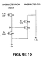
- the unselected column sourceline has a 3.25 volt supplied. This places an approximately 3 volt charge onto the source node SN and the result is that there is insufficient voltage across the breakdown transistor and the breakdown transistor M0 is not programmed.
- the program wordline is at 3.25 volts and the write wordline is at zero volts.
- Node SN will charge up if the breakdown transistor M0 had been previously programmed, but this has no effect. If the breakdown transistor M0 had not been programmed, sense node SN may collect charge through the M1 transistor and possibly through the breakdown transistor, but this will be handled during the read cycle.
- sense node SN will charge up if the breakdown transistor M0 is programmed. But this results in no effect in this case. If the breakdown transistor M0 is unprogrammed, the sense node SN could receive some charge possibly through the breakdown transistor M0, but this is handled in the selected row selected column read cycle.
- the signal on the write wordline may have a short duration positive pulse designed to remove any leakage charge situated on the sense node SN. This will solve the problem of any stray charge on the sense node SN. If the breakdown transistor M0 is programmed, the sense node will be pulled down and then charged back up again through the programmed breakdown transistor M0. This is typically a very short time constant and thus the positive pulse on the write wordline can be made very short. After this is performed, the read wordline is asserted.
Landscapes
- Read Only Memory (AREA)
- Semiconductor Memories (AREA)
- Non-Volatile Memory (AREA)
Claims (7)
- Cellule de mémoire programmable formée d'une manière utile dans une matrice mémoire ayant des lignes de binaires en colonnes et des lignes de mots en rangées, la matrice mémoire comprenant :un transistor de claquage (10) ayant sa porte reliée à une ligne de mots de programme (WP),un transistor d'écriture (41) monté en série à un noeud de détection (SN) audit transistor de claquage (10), ledit transistor d'écriture (41) ayant sa porte reliée à une ligne de mots d'écriture (WW),un premier transistor de détection (42) ayant sa porte reliée audit noeud de détection ; etun deuxième transistor de détection (43) monté en série avec ledit premier transistor de détection etcaractérisé en ce que sa porte est reliée à une ligne de mots de lecture (WR), ledit deuxième transistor de détection ayant sa source reliée à une ligne de binaire en colonne (BL).
- Cellule de mémoire selon la revendication 1, où ledit transistor d'écriture (41) a sa source reliée à une ligne de sources en colonne (SL).
- Cellule de mémoire selon la revendication 2, où ledit premier transistor de détection (42) a sa source reliée à une ligne de sources en colonne (SL).
- Cellule de mémoire selon la revendication 1, où le drain dudit premier transistor de détection (42) est relié à la source dudit deuxième transistor de détection (43).
- Cellule de mémoire selon la revendication 1, où ledit transistor de claquage (40) est remplacé par une capacité MOS ou capacité polysilicone-oxyde-semiconductrice, et ladite ligne de mots programme (WP) est reliée à un polysilicone ou une couche métallique de ladite capacité.
- Cellule de mémoire selon la revendication 1, où ladite cellule de mémoire est programmée en appliquant une tension de programme VPP à ladite ligne de mots programme (WP) et en mettant en service ledit transistor d'écriture (41) pour permettre au courant de programmation de passer à travers ledit transistor de claquage (40) et sur une ligne de sources en colonne (SL).
- Cellule de mémoire selon la revendication 1, où ladite cellule de mémoire est lue en mettant hors service ledit transistor d'écriture (41), en appliquant une tension de lecture (VRD) à ladite ligne de mots programme (WP) et VDD à la porte du second transistor de détection (43), où ladite ligne de binaires en colonne (BL) aura une tension décroissante si ladite cellule de mémoire est programmée et une tension stable si ladite cellule de mémoire n'est pas programmée.
Applications Claiming Priority (1)
| Application Number | Priority Date | Filing Date | Title |
|---|---|---|---|
| US11/252,461 US7173851B1 (en) | 2005-10-18 | 2005-10-18 | 3.5 transistor non-volatile memory cell using gate breakdown phenomena |
Publications (2)
| Publication Number | Publication Date |
|---|---|
| EP1777708A1 EP1777708A1 (fr) | 2007-04-25 |
| EP1777708B1 true EP1777708B1 (fr) | 2008-05-28 |
Family
ID=37669942
Family Applications (1)
| Application Number | Title | Priority Date | Filing Date |
|---|---|---|---|
| EP06251693A Expired - Lifetime EP1777708B1 (fr) | 2005-10-18 | 2006-03-28 | Cellule de mémoire non-volatile à 3,5 transistors utilisant le phénomène de claquage |
Country Status (7)
| Country | Link |
|---|---|
| US (1) | US7173851B1 (fr) |
| EP (1) | EP1777708B1 (fr) |
| JP (1) | JP5043357B2 (fr) |
| CN (1) | CN100527280C (fr) |
| AT (1) | ATE397274T1 (fr) |
| DE (1) | DE602006001343D1 (fr) |
| TW (1) | TWI303424B (fr) |
Cited By (1)
| Publication number | Priority date | Publication date | Assignee | Title |
|---|---|---|---|---|
| US11251189B2 (en) | 2009-02-09 | 2022-02-15 | Longitude Flash Memory Solutions Ltd. | Gate fringing effect based channel formation for semiconductor device |
Families Citing this family (42)
| Publication number | Priority date | Publication date | Assignee | Title |
|---|---|---|---|---|
| US7869790B2 (en) * | 2004-09-24 | 2011-01-11 | Scenera Technologies, Llc | Policy-based controls for wireless cameras |
| US7593248B2 (en) | 2006-11-16 | 2009-09-22 | Aptina Imaging Corporation | Method, apparatus and system providing a one-time programmable memory device |
| US7875840B2 (en) * | 2006-11-16 | 2011-01-25 | Aptina Imaging Corporation | Imager device with anti-fuse pixels and recessed color filter array |
| US20080117661A1 (en) * | 2006-11-16 | 2008-05-22 | Micron Technology, Inc. | Method, apparatus and system providing memory cells associated with a pixel array |
| EP2172082B1 (fr) * | 2007-06-19 | 2020-10-14 | Silicon Line GmbH | Circuiterie et procédé pour commander des composants électroluminescents |
| WO2008155385A1 (fr) * | 2007-06-19 | 2008-12-24 | Silicon Line Gmbh | Circuiterie et procédé pour commander des composants électroluminescents |
| WO2009007464A1 (fr) * | 2007-07-12 | 2009-01-15 | Silicon Line Gmbh | Circuit et procédé d'excitation d'au moins un conducteur différentiel |
| JP5591792B2 (ja) * | 2008-04-16 | 2014-09-17 | シリコン・ライン・ゲー・エム・ベー・ハー | プログラマブルアンチヒューズトランジスタ及びそのプログラム方法 |
| JP5489180B2 (ja) * | 2008-05-21 | 2014-05-14 | シリコン・ライン・ゲー・エム・ベー・ハー | 発光コンポーネントを制御するための回路構造と方法 |
| US7808831B2 (en) * | 2008-06-30 | 2010-10-05 | Sandisk Corporation | Read disturb mitigation in non-volatile memory |
| CN101359505B (zh) * | 2008-09-02 | 2011-04-20 | 北京芯技佳易微电子科技有限公司 | 一种读隔离可编程存储器单元及其编程和读取方法 |
| WO2010040816A2 (fr) | 2008-10-09 | 2010-04-15 | Silicon Line Gmbh | Circuit et procédé de transmission de signaux codés tmds |
| US8208312B1 (en) | 2009-09-22 | 2012-06-26 | Novocell Semiconductor, Inc. | Non-volatile memory element integratable with standard CMOS circuitry |
| US8199590B1 (en) | 2009-09-25 | 2012-06-12 | Novocell Semiconductor, Inc. | Multiple time programmable non-volatile memory element |
| US8134859B1 (en) | 2009-09-25 | 2012-03-13 | Novocell Semiconductor, Inc. | Method of sensing a programmable non-volatile memory element |
| KR20130095554A (ko) | 2012-02-20 | 2013-08-28 | 삼성전자주식회사 | 안티 퓨즈 회로 및 이를 포함하는 반도체 장치 |
| US8797808B2 (en) | 2012-05-30 | 2014-08-05 | SK Hynix Inc. | Semiconductor device and semiconductor memory device |
| US8787106B2 (en) | 2012-07-06 | 2014-07-22 | SK Hynix Inc. | Data storing circuit and repair circuit of memory device including the same |
| US9728235B2 (en) | 2012-07-17 | 2017-08-08 | SK Hynix Inc. | Semiconductor device and semiconductor memory device |
| US8788893B2 (en) | 2012-08-28 | 2014-07-22 | SK Hynix Inc. | Semiconductor device and memory device |
| US9015463B2 (en) | 2012-08-31 | 2015-04-21 | SK Hynix Inc. | Memory device, memory system including a non-volatile memory configured to output a repair data in response to an initialization signal |
| US8867288B2 (en) | 2012-11-08 | 2014-10-21 | SK Hynix Inc. | Memory device and test method thereof |
| US8817519B2 (en) * | 2012-11-08 | 2014-08-26 | SK Hynix Inc. | Integrated circuit including e-fuse array circuit |
| US8913451B2 (en) | 2012-11-08 | 2014-12-16 | SK Hynix Inc. | Memory device and test method thereof |
| US8885424B2 (en) | 2012-11-08 | 2014-11-11 | SK Hynix Inc. | Integrated circuit and memory device |
| US9165620B2 (en) | 2012-11-08 | 2015-10-20 | SK Hynix Inc. | Memory system and operating method thereof |
| KR102031147B1 (ko) | 2013-04-04 | 2019-10-14 | 에스케이하이닉스 주식회사 | 메모리 장치, 메모리 장치 및 메모리 시스템의 동작방법 |
| KR102031191B1 (ko) | 2013-04-17 | 2019-10-11 | 에스케이하이닉스 주식회사 | 비휘발성 메모리 및 이의 부트업 동작 방법 |
| KR20140124547A (ko) | 2013-04-17 | 2014-10-27 | 에스케이하이닉스 주식회사 | 메모리 장치 및 이를 포함하는 메모리 시스템 |
| KR102182419B1 (ko) | 2013-06-28 | 2020-11-24 | 에스케이하이닉스 주식회사 | 비휘발성 메모리 및 이를 포함하는 반도체 장치 |
| KR20150040481A (ko) | 2013-10-07 | 2015-04-15 | 에스케이하이닉스 주식회사 | 메모리 장치, 메모리 장치 및 메모리 시스템의 동작방법 |
| KR102103415B1 (ko) | 2013-10-07 | 2020-04-23 | 에스케이하이닉스 주식회사 | 반도체 장치, 메모리 장치 및 이를 포함하는 시스템 |
| KR102141464B1 (ko) | 2013-12-20 | 2020-08-05 | 에스케이하이닉스 주식회사 | 집적회로 및 메모리 장치 |
| KR102156276B1 (ko) | 2014-04-14 | 2020-09-16 | 에스케이하이닉스 주식회사 | 메모리 장치 및 이의 동작 방법 |
| KR20150130608A (ko) | 2014-05-13 | 2015-11-24 | 에스케이하이닉스 주식회사 | 메모리 장치 |
| KR102150477B1 (ko) | 2014-06-16 | 2020-09-01 | 에스케이하이닉스 주식회사 | 반도체 장치 및 이의 동작 방법 |
| KR20160014976A (ko) | 2014-07-30 | 2016-02-12 | 에스케이하이닉스 주식회사 | 메모리 장치 및 이를 포함하는 메모리 시스템 |
| US9362001B2 (en) | 2014-10-14 | 2016-06-07 | Ememory Technology Inc. | Memory cell capable of operating under low voltage conditions |
| KR20160046502A (ko) | 2014-10-21 | 2016-04-29 | 에스케이하이닉스 주식회사 | 메모리 장치 및 이를 포함하는 메모리 시스템 |
| CN109390021B (zh) * | 2017-08-03 | 2022-05-03 | 联华电子股份有限公司 | 只读存储器 |
| US11443819B2 (en) * | 2020-07-24 | 2022-09-13 | Taiwan Semiconductor Manufacturing Company, Ltd. | Memory device, integrated circuit device and method |
| US11557354B2 (en) * | 2021-02-03 | 2023-01-17 | Macronix International Co., Ltd. | Flash memory and flash memory cell thereof |
Family Cites Families (8)
| Publication number | Priority date | Publication date | Assignee | Title |
|---|---|---|---|---|
| JPH0793030B2 (ja) * | 1990-04-06 | 1995-10-09 | 株式会社東芝 | 半導体メモリ装置 |
| US6243294B1 (en) * | 1999-03-05 | 2001-06-05 | Xilinx, Inc. | Memory architecture for non-volatile storage using gate breakdown structure in standard sub 0.35 micron process |
| US6266269B1 (en) * | 2000-06-07 | 2001-07-24 | Xilinx, Inc. | Three terminal non-volatile memory element |
| WO2003025944A1 (fr) * | 2001-09-18 | 2003-03-27 | Kilopass Technologies, Inc. | Cellule de memoire semi-conductrice et matrice memoire utilisant un phenomene de claquage dans un dielectrique ultra-mince |
| US6798693B2 (en) * | 2001-09-18 | 2004-09-28 | Kilopass Technologies, Inc. | Semiconductor memory cell and memory array using a breakdown phenomena in an ultra-thin dielectric |
| KR100500579B1 (ko) * | 2003-06-28 | 2005-07-12 | 한국과학기술원 | 씨모스 게이트 산화물 안티퓨즈를 이용한 3-트랜지스터한번 프로그램 가능한 롬 |
| US7064973B2 (en) * | 2004-02-03 | 2006-06-20 | Klp International, Ltd. | Combination field programmable gate array allowing dynamic reprogrammability |
| US6972986B2 (en) * | 2004-02-03 | 2005-12-06 | Kilopass Technologies, Inc. | Combination field programmable gate array allowing dynamic reprogrammability and non-votatile programmability based upon transistor gate oxide breakdown |
-
2005
- 2005-10-18 US US11/252,461 patent/US7173851B1/en not_active Expired - Lifetime
-
2006
- 2006-03-13 TW TW095108467A patent/TWI303424B/zh active
- 2006-03-28 DE DE602006001343T patent/DE602006001343D1/de not_active Expired - Lifetime
- 2006-03-28 AT AT06251693T patent/ATE397274T1/de not_active IP Right Cessation
- 2006-03-28 EP EP06251693A patent/EP1777708B1/fr not_active Expired - Lifetime
- 2006-04-04 JP JP2006102753A patent/JP5043357B2/ja not_active Expired - Lifetime
- 2006-10-18 CN CNB2006101425131A patent/CN100527280C/zh active Active
Cited By (2)
| Publication number | Priority date | Publication date | Assignee | Title |
|---|---|---|---|---|
| US11251189B2 (en) | 2009-02-09 | 2022-02-15 | Longitude Flash Memory Solutions Ltd. | Gate fringing effect based channel formation for semiconductor device |
| US11950412B2 (en) | 2009-02-09 | 2024-04-02 | Longitude Flash Memory Solutions Ltd. | Gate fringing effect based channel formation for semiconductor device |
Also Published As
| Publication number | Publication date |
|---|---|
| TWI303424B (en) | 2008-11-21 |
| CN100527280C (zh) | 2009-08-12 |
| ATE397274T1 (de) | 2008-06-15 |
| TW200717518A (en) | 2007-05-01 |
| CN1983449A (zh) | 2007-06-20 |
| DE602006001343D1 (de) | 2008-07-10 |
| EP1777708A1 (fr) | 2007-04-25 |
| JP5043357B2 (ja) | 2012-10-10 |
| US7173851B1 (en) | 2007-02-06 |
| JP2007116084A (ja) | 2007-05-10 |
Similar Documents
| Publication | Publication Date | Title |
|---|---|---|
| EP1777708B1 (fr) | Cellule de mémoire non-volatile à 3,5 transistors utilisant le phénomène de claquage | |
| US7280397B2 (en) | Three-dimensional non-volatile SRAM incorporating thin-film device layer | |
| US7623368B2 (en) | Non-volatile semiconductor memory based on enhanced gate oxide breakdown | |
| KR100500579B1 (ko) | 씨모스 게이트 산화물 안티퓨즈를 이용한 3-트랜지스터한번 프로그램 가능한 롬 | |
| US6972986B2 (en) | Combination field programmable gate array allowing dynamic reprogrammability and non-votatile programmability based upon transistor gate oxide breakdown | |
| EP1583239B1 (fr) | Combinaison de réseaux de portes programmables permettant reprogrammabilité dynamique | |
| US7164608B2 (en) | NVRAM memory cell architecture that integrates conventional SRAM and flash cells | |
| EP1579479B1 (fr) | Cellule memoire semi-conductrice haute densite et reseau memoire utilisant un seul transistor | |
| US9087588B2 (en) | Programmable non-volatile memory | |
| US7492643B2 (en) | Nonvolatile semiconductor memory | |
| US20100110750A1 (en) | Non-volatile semiconductor memory device | |
| TWI484494B (zh) | 單層多晶矽非揮發式記憶體 | |
| US9275753B2 (en) | Circuit and method for reducing write disturb in a non-volatile memory device | |
| EP1290559B1 (fr) | Memoires adressables par le contenu et a double port, destinees au fonctionnement simultane d'une memoire flash | |
| CN114664346A (zh) | 一种反熔丝存储阵列电路及其操作方法以及存储器 | |
| US20250182835A1 (en) | Semiconductor memory devices with diode-connected mos | |
| US6347052B1 (en) | Word line decoding architecture in a flash memory | |
| US6493268B1 (en) | Circuit device for performing hierarchic row decoding in non-volatile memory devices | |
| KR100940198B1 (ko) | 멀티비트 otp 셀 | |
| US6515902B1 (en) | Method and apparatus for boosting bitlines for low VCC read | |
| Cha et al. | A high-density 64k-bit one-time programmable ROM array with 3-transistor cell standard CMOS gate-oxide antifuse | |
| US5838046A (en) | Operating method for ROM array which minimizes band-to-band tunneling |
Legal Events
| Date | Code | Title | Description |
|---|---|---|---|
| PUAI | Public reference made under article 153(3) epc to a published international application that has entered the european phase |
Free format text: ORIGINAL CODE: 0009012 |
|
| AK | Designated contracting states |
Kind code of ref document: A1 Designated state(s): AT BE BG CH CY CZ DE DK EE ES FI FR GB GR HU IE IS IT LI LT LU LV MC NL PL PT RO SE SI SK TR |
|
| AX | Request for extension of the european patent |
Extension state: AL BA HR MK YU |
|
| RAP1 | Party data changed (applicant data changed or rights of an application transferred) |
Owner name: KILOPASS TECHNOLOGY, INC. |
|
| 17P | Request for examination filed |
Effective date: 20070521 |
|
| GRAP | Despatch of communication of intention to grant a patent |
Free format text: ORIGINAL CODE: EPIDOSNIGR1 |
|
| AKX | Designation fees paid |
Designated state(s): AT BE BG CH CY CZ DE DK EE ES FI FR GB GR HU IE IS IT LI LT LU LV MC NL PL PT RO SE SI SK TR |
|
| GRAS | Grant fee paid |
Free format text: ORIGINAL CODE: EPIDOSNIGR3 |
|
| GRAA | (expected) grant |
Free format text: ORIGINAL CODE: 0009210 |
|
| AK | Designated contracting states |
Kind code of ref document: B1 Designated state(s): AT BE BG CH CY CZ DE DK EE ES FI FR GB GR HU IE IS IT LI LT LU LV MC NL PL PT RO SE SI SK TR |
|
| REG | Reference to a national code |
Ref country code: GB Ref legal event code: FG4D |
|
| REG | Reference to a national code |
Ref country code: CH Ref legal event code: EP |
|
| REF | Corresponds to: |
Ref document number: 602006001343 Country of ref document: DE Date of ref document: 20080710 Kind code of ref document: P |
|
| REG | Reference to a national code |
Ref country code: IE Ref legal event code: FG4D |
|
| PG25 | Lapsed in a contracting state [announced via postgrant information from national office to epo] |
Ref country code: SI Free format text: LAPSE BECAUSE OF FAILURE TO SUBMIT A TRANSLATION OF THE DESCRIPTION OR TO PAY THE FEE WITHIN THE PRESCRIBED TIME-LIMIT Effective date: 20080528 |
|
| PG25 | Lapsed in a contracting state [announced via postgrant information from national office to epo] |
Ref country code: FI Free format text: LAPSE BECAUSE OF FAILURE TO SUBMIT A TRANSLATION OF THE DESCRIPTION OR TO PAY THE FEE WITHIN THE PRESCRIBED TIME-LIMIT Effective date: 20080528 Ref country code: ES Free format text: LAPSE BECAUSE OF FAILURE TO SUBMIT A TRANSLATION OF THE DESCRIPTION OR TO PAY THE FEE WITHIN THE PRESCRIBED TIME-LIMIT Effective date: 20080908 |
|
| PG25 | Lapsed in a contracting state [announced via postgrant information from national office to epo] |
Ref country code: NL Free format text: LAPSE BECAUSE OF FAILURE TO SUBMIT A TRANSLATION OF THE DESCRIPTION OR TO PAY THE FEE WITHIN THE PRESCRIBED TIME-LIMIT Effective date: 20080528 Ref country code: AT Free format text: LAPSE BECAUSE OF FAILURE TO SUBMIT A TRANSLATION OF THE DESCRIPTION OR TO PAY THE FEE WITHIN THE PRESCRIBED TIME-LIMIT Effective date: 20080528 Ref country code: LV Free format text: LAPSE BECAUSE OF FAILURE TO SUBMIT A TRANSLATION OF THE DESCRIPTION OR TO PAY THE FEE WITHIN THE PRESCRIBED TIME-LIMIT Effective date: 20080528 |
|
| NLV1 | Nl: lapsed or annulled due to failure to fulfill the requirements of art. 29p and 29m of the patents act | ||
| PG25 | Lapsed in a contracting state [announced via postgrant information from national office to epo] |
Ref country code: IS Free format text: LAPSE BECAUSE OF FAILURE TO SUBMIT A TRANSLATION OF THE DESCRIPTION OR TO PAY THE FEE WITHIN THE PRESCRIBED TIME-LIMIT Effective date: 20080928 |
|
| PG25 | Lapsed in a contracting state [announced via postgrant information from national office to epo] |
Ref country code: SE Free format text: LAPSE BECAUSE OF FAILURE TO SUBMIT A TRANSLATION OF THE DESCRIPTION OR TO PAY THE FEE WITHIN THE PRESCRIBED TIME-LIMIT Effective date: 20080828 Ref country code: LT Free format text: LAPSE BECAUSE OF FAILURE TO SUBMIT A TRANSLATION OF THE DESCRIPTION OR TO PAY THE FEE WITHIN THE PRESCRIBED TIME-LIMIT Effective date: 20080528 Ref country code: DK Free format text: LAPSE BECAUSE OF FAILURE TO SUBMIT A TRANSLATION OF THE DESCRIPTION OR TO PAY THE FEE WITHIN THE PRESCRIBED TIME-LIMIT Effective date: 20080528 Ref country code: CZ Free format text: LAPSE BECAUSE OF FAILURE TO SUBMIT A TRANSLATION OF THE DESCRIPTION OR TO PAY THE FEE WITHIN THE PRESCRIBED TIME-LIMIT Effective date: 20080528 |
|
| PG25 | Lapsed in a contracting state [announced via postgrant information from national office to epo] |
Ref country code: PT Free format text: LAPSE BECAUSE OF FAILURE TO SUBMIT A TRANSLATION OF THE DESCRIPTION OR TO PAY THE FEE WITHIN THE PRESCRIBED TIME-LIMIT Effective date: 20081028 Ref country code: BE Free format text: LAPSE BECAUSE OF FAILURE TO SUBMIT A TRANSLATION OF THE DESCRIPTION OR TO PAY THE FEE WITHIN THE PRESCRIBED TIME-LIMIT Effective date: 20080528 Ref country code: RO Free format text: LAPSE BECAUSE OF FAILURE TO SUBMIT A TRANSLATION OF THE DESCRIPTION OR TO PAY THE FEE WITHIN THE PRESCRIBED TIME-LIMIT Effective date: 20080528 Ref country code: SK Free format text: LAPSE BECAUSE OF FAILURE TO SUBMIT A TRANSLATION OF THE DESCRIPTION OR TO PAY THE FEE WITHIN THE PRESCRIBED TIME-LIMIT Effective date: 20080528 |
|
| PLBE | No opposition filed within time limit |
Free format text: ORIGINAL CODE: 0009261 |
|
| PG25 | Lapsed in a contracting state [announced via postgrant information from national office to epo] |
Ref country code: BG Free format text: LAPSE BECAUSE OF FAILURE TO SUBMIT A TRANSLATION OF THE DESCRIPTION OR TO PAY THE FEE WITHIN THE PRESCRIBED TIME-LIMIT Effective date: 20080828 Ref country code: EE Free format text: LAPSE BECAUSE OF FAILURE TO SUBMIT A TRANSLATION OF THE DESCRIPTION OR TO PAY THE FEE WITHIN THE PRESCRIBED TIME-LIMIT Effective date: 20080528 |
|
| 26N | No opposition filed |
Effective date: 20090303 |
|
| PG25 | Lapsed in a contracting state [announced via postgrant information from national office to epo] |
Ref country code: IT Free format text: LAPSE BECAUSE OF FAILURE TO SUBMIT A TRANSLATION OF THE DESCRIPTION OR TO PAY THE FEE WITHIN THE PRESCRIBED TIME-LIMIT Effective date: 20080528 |
|
| PG25 | Lapsed in a contracting state [announced via postgrant information from national office to epo] |
Ref country code: MC Free format text: LAPSE BECAUSE OF NON-PAYMENT OF DUE FEES Effective date: 20090331 |
|
| REG | Reference to a national code |
Ref country code: IE Ref legal event code: MM4A |
|
| PG25 | Lapsed in a contracting state [announced via postgrant information from national office to epo] |
Ref country code: IE Free format text: LAPSE BECAUSE OF NON-PAYMENT OF DUE FEES Effective date: 20090328 |
|
| PG25 | Lapsed in a contracting state [announced via postgrant information from national office to epo] |
Ref country code: PL Free format text: LAPSE BECAUSE OF FAILURE TO SUBMIT A TRANSLATION OF THE DESCRIPTION OR TO PAY THE FEE WITHIN THE PRESCRIBED TIME-LIMIT Effective date: 20080528 |
|
| PG25 | Lapsed in a contracting state [announced via postgrant information from national office to epo] |
Ref country code: GR Free format text: LAPSE BECAUSE OF FAILURE TO SUBMIT A TRANSLATION OF THE DESCRIPTION OR TO PAY THE FEE WITHIN THE PRESCRIBED TIME-LIMIT Effective date: 20080829 |
|
| REG | Reference to a national code |
Ref country code: CH Ref legal event code: PL |
|
| PG25 | Lapsed in a contracting state [announced via postgrant information from national office to epo] |
Ref country code: CH Free format text: LAPSE BECAUSE OF NON-PAYMENT OF DUE FEES Effective date: 20100331 Ref country code: LI Free format text: LAPSE BECAUSE OF NON-PAYMENT OF DUE FEES Effective date: 20100331 |
|
| PG25 | Lapsed in a contracting state [announced via postgrant information from national office to epo] |
Ref country code: LU Free format text: LAPSE BECAUSE OF NON-PAYMENT OF DUE FEES Effective date: 20090328 |
|
| PG25 | Lapsed in a contracting state [announced via postgrant information from national office to epo] |
Ref country code: HU Free format text: LAPSE BECAUSE OF FAILURE TO SUBMIT A TRANSLATION OF THE DESCRIPTION OR TO PAY THE FEE WITHIN THE PRESCRIBED TIME-LIMIT Effective date: 20081129 |
|
| PG25 | Lapsed in a contracting state [announced via postgrant information from national office to epo] |
Ref country code: TR Free format text: LAPSE BECAUSE OF FAILURE TO SUBMIT A TRANSLATION OF THE DESCRIPTION OR TO PAY THE FEE WITHIN THE PRESCRIBED TIME-LIMIT Effective date: 20080528 |
|
| PG25 | Lapsed in a contracting state [announced via postgrant information from national office to epo] |
Ref country code: CY Free format text: LAPSE BECAUSE OF FAILURE TO SUBMIT A TRANSLATION OF THE DESCRIPTION OR TO PAY THE FEE WITHIN THE PRESCRIBED TIME-LIMIT Effective date: 20080528 |
|
| REG | Reference to a national code |
Ref country code: FR Ref legal event code: PLFP Year of fee payment: 11 |
|
| REG | Reference to a national code |
Ref country code: FR Ref legal event code: PLFP Year of fee payment: 12 |
|
| REG | Reference to a national code |
Ref country code: FR Ref legal event code: PLFP Year of fee payment: 13 |
|
| REG | Reference to a national code |
Ref country code: DE Ref legal event code: R082 Ref document number: 602006001343 Country of ref document: DE Representative=s name: LEINWEBER & ZIMMERMANN, DE Ref country code: DE Ref legal event code: R081 Ref document number: 602006001343 Country of ref document: DE Owner name: SYNOPSYS, INC. (N.D.GES.D. STAATES DELAWARE), , US Free format text: FORMER OWNER: KILOPASS TECHNOLOGIES, INC., SANTA CLARA, CALIF., US Ref country code: DE Ref legal event code: R082 Ref document number: 602006001343 Country of ref document: DE Representative=s name: LEINWEBER & ZIMMERMANN PATENTANWALTS-PARTG MBB, DE |
|
| REG | Reference to a national code |
Ref country code: GB Ref legal event code: 732E Free format text: REGISTERED BETWEEN 20190131 AND 20190206 |
|
| P01 | Opt-out of the competence of the unified patent court (upc) registered |
Effective date: 20230528 |
|
| PGFP | Annual fee paid to national office [announced via postgrant information from national office to epo] |
Ref country code: DE Payment date: 20250218 Year of fee payment: 20 |
|
| PGFP | Annual fee paid to national office [announced via postgrant information from national office to epo] |
Ref country code: FR Payment date: 20250218 Year of fee payment: 20 |
|
| PGFP | Annual fee paid to national office [announced via postgrant information from national office to epo] |
Ref country code: GB Payment date: 20250221 Year of fee payment: 20 |
|
| REG | Reference to a national code |
Ref country code: DE Ref legal event code: R071 Ref document number: 602006001343 Country of ref document: DE |
|
| REG | Reference to a national code |
Ref country code: GB Ref legal event code: PE20 Expiry date: 20260327 |