EP1780017A2 - Tête d'imprimante à jet d'encre piézoélectrique - Google Patents
Tête d'imprimante à jet d'encre piézoélectrique Download PDFInfo
- Publication number
- EP1780017A2 EP1780017A2 EP07101257A EP07101257A EP1780017A2 EP 1780017 A2 EP1780017 A2 EP 1780017A2 EP 07101257 A EP07101257 A EP 07101257A EP 07101257 A EP07101257 A EP 07101257A EP 1780017 A2 EP1780017 A2 EP 1780017A2
- Authority
- EP
- European Patent Office
- Prior art keywords
- ink
- flow path
- piezoelectric
- inkjet printhead
- temperature detector
- Prior art date
- Legal status (The legal status is an assumption and is not a legal conclusion. Google has not performed a legal analysis and makes no representation as to the accuracy of the status listed.)
- Granted
Links
Images




Classifications
-
- C—CHEMISTRY; METALLURGY
- C30—CRYSTAL GROWTH
- C30B—SINGLE-CRYSTAL GROWTH; UNIDIRECTIONAL SOLIDIFICATION OF EUTECTIC MATERIAL OR UNIDIRECTIONAL DEMIXING OF EUTECTOID MATERIAL; REFINING BY ZONE-MELTING OF MATERIAL; PRODUCTION OF A HOMOGENEOUS POLYCRYSTALLINE MATERIAL WITH DEFINED STRUCTURE; SINGLE CRYSTALS OR HOMOGENEOUS POLYCRYSTALLINE MATERIAL WITH DEFINED STRUCTURE; AFTER-TREATMENT OF SINGLE CRYSTALS OR A HOMOGENEOUS POLYCRYSTALLINE MATERIAL WITH DEFINED STRUCTURE; APPARATUS THEREFOR
- C30B23/00—Single-crystal growth by condensing evaporated or sublimed materials
-
- B—PERFORMING OPERATIONS; TRANSPORTING
- B41—PRINTING; LINING MACHINES; TYPEWRITERS; STAMPS
- B41J—TYPEWRITERS; SELECTIVE PRINTING MECHANISMS, i.e. MECHANISMS PRINTING OTHERWISE THAN FROM A FORME; CORRECTION OF TYPOGRAPHICAL ERRORS
- B41J2/00—Typewriters or selective printing mechanisms characterised by the printing or marking process for which they are designed
- B41J2/005—Typewriters or selective printing mechanisms characterised by the printing or marking process for which they are designed characterised by bringing liquid or particles selectively into contact with a printing material
- B41J2/01—Ink jet
- B41J2/135—Nozzles
- B41J2/16—Production of nozzles
- B41J2/1607—Production of print heads with piezoelectric elements
- B41J2/161—Production of print heads with piezoelectric elements of film type, deformed by bending and disposed on a diaphragm
-
- B—PERFORMING OPERATIONS; TRANSPORTING
- B41—PRINTING; LINING MACHINES; TYPEWRITERS; STAMPS
- B41J—TYPEWRITERS; SELECTIVE PRINTING MECHANISMS, i.e. MECHANISMS PRINTING OTHERWISE THAN FROM A FORME; CORRECTION OF TYPOGRAPHICAL ERRORS
- B41J2/00—Typewriters or selective printing mechanisms characterised by the printing or marking process for which they are designed
- B41J2/005—Typewriters or selective printing mechanisms characterised by the printing or marking process for which they are designed characterised by bringing liquid or particles selectively into contact with a printing material
- B41J2/01—Ink jet
- B41J2/135—Nozzles
- B41J2/14—Structure thereof only for on-demand ink jet heads
- B41J2/14016—Structure of bubble jet print heads
- B41J2/14088—Structure of heating means
- B41J2/14112—Resistive element
- B41J2/14137—Resistor surrounding the nozzle opening
-
- B—PERFORMING OPERATIONS; TRANSPORTING
- B41—PRINTING; LINING MACHINES; TYPEWRITERS; STAMPS
- B41J—TYPEWRITERS; SELECTIVE PRINTING MECHANISMS, i.e. MECHANISMS PRINTING OTHERWISE THAN FROM A FORME; CORRECTION OF TYPOGRAPHICAL ERRORS
- B41J2/00—Typewriters or selective printing mechanisms characterised by the printing or marking process for which they are designed
- B41J2/005—Typewriters or selective printing mechanisms characterised by the printing or marking process for which they are designed characterised by bringing liquid or particles selectively into contact with a printing material
- B41J2/01—Ink jet
- B41J2/135—Nozzles
- B41J2/14—Structure thereof only for on-demand ink jet heads
- B41J2/14201—Structure of print heads with piezoelectric elements
- B41J2/14233—Structure of print heads with piezoelectric elements of film type, deformed by bending and disposed on a diaphragm
-
- B—PERFORMING OPERATIONS; TRANSPORTING
- B41—PRINTING; LINING MACHINES; TYPEWRITERS; STAMPS
- B41J—TYPEWRITERS; SELECTIVE PRINTING MECHANISMS, i.e. MECHANISMS PRINTING OTHERWISE THAN FROM A FORME; CORRECTION OF TYPOGRAPHICAL ERRORS
- B41J2/00—Typewriters or selective printing mechanisms characterised by the printing or marking process for which they are designed
- B41J2/005—Typewriters or selective printing mechanisms characterised by the printing or marking process for which they are designed characterised by bringing liquid or particles selectively into contact with a printing material
- B41J2/01—Ink jet
- B41J2/135—Nozzles
- B41J2/16—Production of nozzles
- B41J2/162—Manufacturing of the nozzle plates
-
- B—PERFORMING OPERATIONS; TRANSPORTING
- B41—PRINTING; LINING MACHINES; TYPEWRITERS; STAMPS
- B41J—TYPEWRITERS; SELECTIVE PRINTING MECHANISMS, i.e. MECHANISMS PRINTING OTHERWISE THAN FROM A FORME; CORRECTION OF TYPOGRAPHICAL ERRORS
- B41J2/00—Typewriters or selective printing mechanisms characterised by the printing or marking process for which they are designed
- B41J2/005—Typewriters or selective printing mechanisms characterised by the printing or marking process for which they are designed characterised by bringing liquid or particles selectively into contact with a printing material
- B41J2/01—Ink jet
- B41J2/135—Nozzles
- B41J2/16—Production of nozzles
- B41J2/1621—Manufacturing processes
- B41J2/1623—Manufacturing processes bonding and adhesion
-
- B—PERFORMING OPERATIONS; TRANSPORTING
- B41—PRINTING; LINING MACHINES; TYPEWRITERS; STAMPS
- B41J—TYPEWRITERS; SELECTIVE PRINTING MECHANISMS, i.e. MECHANISMS PRINTING OTHERWISE THAN FROM A FORME; CORRECTION OF TYPOGRAPHICAL ERRORS
- B41J2/00—Typewriters or selective printing mechanisms characterised by the printing or marking process for which they are designed
- B41J2/005—Typewriters or selective printing mechanisms characterised by the printing or marking process for which they are designed characterised by bringing liquid or particles selectively into contact with a printing material
- B41J2/01—Ink jet
- B41J2/135—Nozzles
- B41J2/16—Production of nozzles
- B41J2/1621—Manufacturing processes
- B41J2/1626—Manufacturing processes etching
- B41J2/1628—Manufacturing processes etching dry etching
-
- B—PERFORMING OPERATIONS; TRANSPORTING
- B41—PRINTING; LINING MACHINES; TYPEWRITERS; STAMPS
- B41J—TYPEWRITERS; SELECTIVE PRINTING MECHANISMS, i.e. MECHANISMS PRINTING OTHERWISE THAN FROM A FORME; CORRECTION OF TYPOGRAPHICAL ERRORS
- B41J2/00—Typewriters or selective printing mechanisms characterised by the printing or marking process for which they are designed
- B41J2/005—Typewriters or selective printing mechanisms characterised by the printing or marking process for which they are designed characterised by bringing liquid or particles selectively into contact with a printing material
- B41J2/01—Ink jet
- B41J2/135—Nozzles
- B41J2/16—Production of nozzles
- B41J2/1621—Manufacturing processes
- B41J2/1626—Manufacturing processes etching
- B41J2/1629—Manufacturing processes etching wet etching
-
- B—PERFORMING OPERATIONS; TRANSPORTING
- B41—PRINTING; LINING MACHINES; TYPEWRITERS; STAMPS
- B41J—TYPEWRITERS; SELECTIVE PRINTING MECHANISMS, i.e. MECHANISMS PRINTING OTHERWISE THAN FROM A FORME; CORRECTION OF TYPOGRAPHICAL ERRORS
- B41J2/00—Typewriters or selective printing mechanisms characterised by the printing or marking process for which they are designed
- B41J2/005—Typewriters or selective printing mechanisms characterised by the printing or marking process for which they are designed characterised by bringing liquid or particles selectively into contact with a printing material
- B41J2/01—Ink jet
- B41J2/135—Nozzles
- B41J2/16—Production of nozzles
- B41J2/1621—Manufacturing processes
- B41J2/1631—Manufacturing processes photolithography
-
- B—PERFORMING OPERATIONS; TRANSPORTING
- B41—PRINTING; LINING MACHINES; TYPEWRITERS; STAMPS
- B41J—TYPEWRITERS; SELECTIVE PRINTING MECHANISMS, i.e. MECHANISMS PRINTING OTHERWISE THAN FROM A FORME; CORRECTION OF TYPOGRAPHICAL ERRORS
- B41J2/00—Typewriters or selective printing mechanisms characterised by the printing or marking process for which they are designed
- B41J2/005—Typewriters or selective printing mechanisms characterised by the printing or marking process for which they are designed characterised by bringing liquid or particles selectively into contact with a printing material
- B41J2/01—Ink jet
- B41J2/135—Nozzles
- B41J2/16—Production of nozzles
- B41J2/1621—Manufacturing processes
- B41J2/1632—Manufacturing processes machining
-
- B—PERFORMING OPERATIONS; TRANSPORTING
- B41—PRINTING; LINING MACHINES; TYPEWRITERS; STAMPS
- B41J—TYPEWRITERS; SELECTIVE PRINTING MECHANISMS, i.e. MECHANISMS PRINTING OTHERWISE THAN FROM A FORME; CORRECTION OF TYPOGRAPHICAL ERRORS
- B41J2/00—Typewriters or selective printing mechanisms characterised by the printing or marking process for which they are designed
- B41J2/005—Typewriters or selective printing mechanisms characterised by the printing or marking process for which they are designed characterised by bringing liquid or particles selectively into contact with a printing material
- B41J2/01—Ink jet
- B41J2/135—Nozzles
- B41J2/16—Production of nozzles
- B41J2/1621—Manufacturing processes
- B41J2/164—Manufacturing processes thin film formation
- B41J2/1642—Manufacturing processes thin film formation thin film formation by CVD [chemical vapor deposition]
-
- B—PERFORMING OPERATIONS; TRANSPORTING
- B41—PRINTING; LINING MACHINES; TYPEWRITERS; STAMPS
- B41J—TYPEWRITERS; SELECTIVE PRINTING MECHANISMS, i.e. MECHANISMS PRINTING OTHERWISE THAN FROM A FORME; CORRECTION OF TYPOGRAPHICAL ERRORS
- B41J2/00—Typewriters or selective printing mechanisms characterised by the printing or marking process for which they are designed
- B41J2/005—Typewriters or selective printing mechanisms characterised by the printing or marking process for which they are designed characterised by bringing liquid or particles selectively into contact with a printing material
- B41J2/01—Ink jet
- B41J2/135—Nozzles
- B41J2/16—Production of nozzles
- B41J2/1621—Manufacturing processes
- B41J2/164—Manufacturing processes thin film formation
- B41J2/1643—Manufacturing processes thin film formation thin film formation by plating
-
- B—PERFORMING OPERATIONS; TRANSPORTING
- B41—PRINTING; LINING MACHINES; TYPEWRITERS; STAMPS
- B41J—TYPEWRITERS; SELECTIVE PRINTING MECHANISMS, i.e. MECHANISMS PRINTING OTHERWISE THAN FROM A FORME; CORRECTION OF TYPOGRAPHICAL ERRORS
- B41J2/00—Typewriters or selective printing mechanisms characterised by the printing or marking process for which they are designed
- B41J2/005—Typewriters or selective printing mechanisms characterised by the printing or marking process for which they are designed characterised by bringing liquid or particles selectively into contact with a printing material
- B41J2/01—Ink jet
- B41J2/135—Nozzles
- B41J2/16—Production of nozzles
- B41J2/1621—Manufacturing processes
- B41J2/164—Manufacturing processes thin film formation
- B41J2/1646—Manufacturing processes thin film formation thin film formation by sputtering
-
- C—CHEMISTRY; METALLURGY
- C30—CRYSTAL GROWTH
- C30B—SINGLE-CRYSTAL GROWTH; UNIDIRECTIONAL SOLIDIFICATION OF EUTECTIC MATERIAL OR UNIDIRECTIONAL DEMIXING OF EUTECTOID MATERIAL; REFINING BY ZONE-MELTING OF MATERIAL; PRODUCTION OF A HOMOGENEOUS POLYCRYSTALLINE MATERIAL WITH DEFINED STRUCTURE; SINGLE CRYSTALS OR HOMOGENEOUS POLYCRYSTALLINE MATERIAL WITH DEFINED STRUCTURE; AFTER-TREATMENT OF SINGLE CRYSTALS OR A HOMOGENEOUS POLYCRYSTALLINE MATERIAL WITH DEFINED STRUCTURE; APPARATUS THEREFOR
- C30B29/00—Single crystals or homogeneous polycrystalline material with defined structure characterised by the material or by their shape
- C30B29/10—Inorganic compounds or compositions
- C30B29/36—Carbides
Definitions
- the present invention relates to a piezoelectric inkjet printhead, and more particularly, to a piezoelectric inkjet printhead including a nozzle plate integrally formed with a heater for heating ink and a method of manufacturing the nozzle plate.
- an inkjet printhead is a device that ejects ink droplets at a desired position on a recording medium thereby printing a desired color image.
- the inkjet printhead can be classified into a thermal inkjet printhead and a piezoelectric inkjet printhead.
- the thermal inkjet printhead ink is heated to form ink bubbles and the expansive force of the bubbles causes ink droplets to be ejected.
- the piezoelectric inkjet printhead the deformation of a piezoelectric crystal pushes ink droplets onto a recording medium.
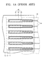
- FIG. 1A is a plan view that illustrates a common construction of a conventional piezoelectric inkjet printhead and FIG. 1B is a vertical sectional view taken along the longitudinal direction of a piezoelectric layer.
- a flow path plate 10 is formed with ink flow paths including a manifold 13, a plurality of restrictors 12, and a plurality of pressure chambers 11.
- a nozzle plate 20 is formed with a plurality of nozzles 22 corresponding to the respective pressure chambers 11.
- a piezoelectric actuator 40 is disposed at an upper side of the flow path plate 10.
- the manifold 13 is a common passage through which ink from an ink reservoir (not shown) is introduced into the pressure chambers 11.
- the restrictors 12 are individual passages through which ink from the manifold 13 is introduced into the respective pressure chambers 11.
- the pressure chambers 11 are filled with ink to be ejected and are disposed at one or both sides of the manifold 13.
- the volumes of the pressure chambers 11 are changed according to the driving of the piezoelectric actuator 40, thereby generating a change of pressure for ink ejection or introduction.
- upper walls of the pressure chambers 11 of the flow path plate 10 serve as vibrating plates 14 that can be deformed by the piezoelectric actuator 40.
- the piezoelectric actuator 40 includes a lower electrode 41, piezoelectric layers 42, and upper electrodes 43 which are sequentially stacked on the flow path plate 10.
- a silicon oxide layer 31 is formed as an insulating film between the lower electrode 41 and the flow path plate 10.
- the lower electrode 41 is formed on the entire surface of the silicon oxide layer 31 and serves as a common electrode.
- the piezoelectric layers 42 are formed on the lower electrode 41 so that they are positioned at upper sides of the pressure chambers 11.
- the upper electrodes 43 are formed on the piezoelectric layers 42 and serve as driving electrodes applying a voltage to the piezoelectric layers 42.
- a flexible printed circuit (FPC) 50 for voltage application is connected to the upper electrodes 43.
- driving signal lines 51 of the flexible printed circuit 50 are disposed on the upper electrodes 43 and then heated and pressurized, to thereby bond the driving signal lines 51 to upper surfaces of the upper electrodes 43.
- U.S. Patent No. 5,701,148 discloses an ink cartridge in which a heater for heating ink is mounted outside an inkjet printhead.
- a heater for heating ink is mounted outside an inkjet printhead.
- the heater since the heater is located relatively away from a nozzle plate, a temperature profile according to the location of the nozzle plate heated by the heater is not uniform. Therefore, ink temperature of nozzles arranged in the nozzle plate is also non-uniform, thereby causing a variation of the ejection speed and volume of ink droplets through the nozzles.
- the heater separately mounted outside the inkjet printhead increases the complexity and size of the ink cartridge.
- U.S. Patent No. 6,074,033 discloses a technique of controlling printing quality by detecting an ambient temperature using a thermistor and estimating physical properties of ink from the detection result.
- this technique has a disadvantage in that an ink temperature value estimated from a detected ambient temperature may vary according to the operating condition of a printhead.
- a piezoelectric inkjet printhead including: a flow path plate formed with an ink flow path including a plurality of pressure chambers filled with ink to be ejected; a piezoelectric actuator formed at an upper side of the flow path plate and supplying a driving force for ink ejection to the pressure chambers; a nozzle plate bonded to the flow path plate, a plurality of nozzles for ink ejection from the pressure chambers being bored through the nozzle plate; and a heater formed on a lower surface of the nozzle plate and heating ink in the ink flow path.
- An insulating layer may be formed on a lower surface of the nozzle plate, the heater may be formed in a predetermined pattern on a surface of the insulating layer, and a protection layer for protecting the heater may be formed on surfaces of the insulating layer and the heater.
- Each of the insulating layer and the protection layer may be a silicon oxide layer.
- Bonding pads for bonding a power supply line may be formed at both ends of the heater and may be exposed through contact holes formed in the protection layer.
- the piezoelectric inkjet printhead may further include a temperature detector for detecting a temperature of the ink in the ink flow path.
- the temperature detector may be made of a metal material having a variable resistance with respect to temperature.
- the temperature detector may be formed on a lower surface of the nozzle plate together with the heater.
- the heater and the temperature detector may be made of the same metal material, for example Pt. Bonding pads for bonding a temperature detection signal line may be formed at both ends of the temperature detector.
- the temperature detector may be formed at an upper side of the flow path plate together with the piezoelectric actuator.
- the temperature detector may be formed on the same plane using the same metal material, for example Pt, as a lower electrode of the piezoelectric actuator.
- the temperature detector may be defined by a trench bored through the lower electrode and be insulated from the lower electrode by the trench.
- a connection electrode for connecting the temperature detection signal line to the temperature detector and a dummy piezoelectric layer for supporting the connection electrode may be formed on the lower electrode.
- the piezoelectric inkjet printhead may further include nozzle metal layers formed around orifices of the nozzles on a lower surface of the nozzle plate.
- the nozzle metal layers may have a circular ring shape.
- the heater and the nozzle metal layers may be formed on the same plane using the same metal material, for example Pt.
- Hydrophobic plating layers made of Au may be formed on surfaces of the nozzle metal layers.
- a piezoelectric inkjet printhead including: a flow path plate formed with an ink flow path including a plurality of pressure chambers filled with ink to be ejected; a piezoelectric actuator including a lower electrode formed on an upper surface of the flow path plate, a piezoelectric layer formed on the lower electrode, and an upper electrode formed on the piezoelectric layer and supplying a driving force for ink ejection to the pressure chambers; a nozzle plate bonded to the flow path plate, a plurality of nozzles for ink ejection from the pressure chambers being bored through the nozzle plate; and a temperature detector formed on an upper surface of the flow path plate together with the piezoelectric actuator and detecting a temperature of ink in the ink flow path.
- a method of manufacturing a nozzle plate of a piezoelectric inkjet printhead through which a plurality of nozzles for ink ejection are bored, the method including: (a) preparing a silicon substrate; (b) forming ink guiding portions of the nozzles by partially etching an upper surface of the silicon substrate; (c) coating a photoresist on a lower surface of the silicon substrate followed by patterning; (d) forming a metal layer on a lower surface of the silicon substrate and a surface of the photoresist; (e) lifting off the photoresist and removing the metal layer formed on the surface of the photoresist to form a heater from a residual metal layer; (f) forming a protection layer for protecting the heater on a lower surface of the silicon substrate; and (g) forming openings by partially etching the protection layer and forming ink outlets communicating with the ink guiding portions by etching portions of the silicon substrate exposed through the openings
- the method may further include forming silicon oxide layers as insulating layers on lower and upper surfaces of the silicon substrate before step (b).
- the residual metal layer may form a temperature detector for detecting ink temperature and nozzle metal layers surrounding orifices of the nozzles, in addition to the heater.
- the nozzle metal layers may be exposed through the openings and are used as etching masks for etching the silicon substrate.
- the method may further include forming hydrophobic plating layers on surfaces of the nozzle metal layers, after step (g).
- the hydrophobic plating layers may be formed by electroplating using the nozzle metal layers as seed layers.
- the method may further include forming contact holes intended for exposure of bonding pads formed at both ends of the heater by partially etching the protection layer after step (g).
- a printhead since a printhead has an integrally formed structure of a heater for heating ink and a nozzle plate, it can be manufactured easily and ink therein can be heated to a uniform temperature.
- the present invention thus provides a simple piezoelectric inkjet printhead including a nozzle plate integrally formed with a heater for heating ink. Therefore, ink can be heated to a uniform temperature.
- the present invention also provides a method of manufacturing the nozzle plate.
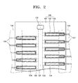
- FIG. 2 is a top plan view of a piezoelectric inkjet printhead according to a first embodiment of the present invention
- FIG. 3 is a bottom plan view of a nozzle plate of the inkjet printhead of FIG. 2
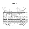
- FIG. 4 is a vertical sectional view taken along line A-A' of FIG. 3.
- the piezoelectric inkjet printhead includes: a flow path plate formed with an ink flow path including pressure chambers 104; a nozzle plate through 130 which nozzles 106 for ink ejection are bored; a piezoelectric actuator 140, disposed on the flow path plate, supplying a driving force for ink ejection to the pressure chambers 104; and a heater 134 for heating ink, integrally formed on a lower surface of the nozzle plate 130.
- the ink flow path includes the pressure chambers 104 filled with ink to be ejected and generating a change of pressure for ink ejection, an ink inlet 101 for ink introduction from an ink reservoir (not shown), a manifold 102 which is a common flow path for ink introduction from the ink inlet 110 into the pressure chambers 104, and restrictors 103 which are individual flow paths for ink introduction from the manifold 102 into the respective pressure chambers 104.
- dampers 105 may be provided between the pressure chambers 104 and the nozzles 106 formed in the nozzle plate 130, to concentrate energy generated in the pressure chambers 104 by the piezoelectric actuator 140 toward the nozzles 106 and to prevent a rapid pressure change.
- These constitutional elements for the ink flow path are formed in the flow path plate. Vibrating plates 111 that can be deformed as the piezoelectric actuator 140 is driven are disposed at upper sides of the pressure chambers 104.
- the flow path plate may include a first flow path plate 110 and a second flow path plate 120 as shown in FIG. 4.
- the pressure chambers 104 are formed to a predetermined depth from a lower surface of the first flow path plate 110 and the ink inlet 101 is bored through one side of the first flow path plate 110.
- the pressure chambers 104 have a cuboidal shape which is longer along an ink flow direction and are arranged in two arrays at both sides of the manifold 102 formed in the second flow path plate 120.
- the pressure chambers 104 may also be arranged in one array at one side of the manifold 102.
- the second flow path plate 120 is formed with the manifold 102. An end of the manifold 102 is connected to the ink inlet 101.
- the manifold 102 may be formed to a predetermined depth from an upper surface of the second flow path plate 120, as shown in FIG. 4. Alternatively, the manifold 102 may be vertically bored through the second flow path plate 120.
- the second flow path plate 120 is also formed with the restrictors 103 which are individual flow paths connecting the manifold 102 and respective one ends of the pressure chambers 104. Like the manifold 102, the restrictors 103 may be formed to a predetermined depth from an upper surface of the second flow path plate 120, as shown in FIG. 4, or may be vertically bored through the second flow path plate 120.
- the dampers 105 connecting the pressure chambers 104 and the nozzles 106 are bored through the second flow path plate 120 corresponding to the other ends of the pressure chambers 104.
- constitutional elements for the ink flow path are arranged in the two flow path plates 110 and 120, this arrangement has been provided only for illustration purposes. That is, the constitutional elements for the ink flow path can have different arrangements in a piezoelectric inkjet printhead of the present invention. These constitutional elements for the ink flow path may also be arranged in only one plate or in three or more plates, instead of the two flow path plates 110 and 120.
- the piezoelectric actuator 140 is formed at an upper side of the first flow path plate 110 with the pressure chambers 104 to supply a driving force for ink ejection to the pressure chambers 104.
- the piezoelectric actuator 140 includes a lower electrode 141 used as a common electrode, piezoelectric layers 142 that are deformed by an applied voltage, and upper electrodes 143 used as driving electrodes.
- the piezoelectric actuator 140 has a sequentially stacked structure of the lower electrode 141, the piezoelectric layers 142, and the upper electrodes 143 on the first flow path plate110.
- an insulating layer 112 is formed between the lower electrode 141 and the first flow path plate 110.
- the lower electrode 141 is formed on the entire surface of the insulating layer 112 and may be a single conductive metal material layer. However, it is preferable to form a thin metal bilayer composed of a Ti layer and a Pt layer as the lower electrode 141.
- the lower electrode 141 made of Ti/Pt serves as a common electrode, and at the same time, as a diffusion barrier layer for prevention of inter-diffusion between the underlying first flow path plate 110 and the overlying piezoelectric layers 142.
- the piezoelectric layers 142 are disposed on the lower electrode 141 corresponding to the pressure chambers 104.
- the piezoelectric layers 104 are deformed by an applied voltage, thereby causing bending of the vibrating plates 111 at upper sides of the pressure chambers 104.
- the piezoelectric layers 142 may be made of a piezoelectric material, preferably a PZT (Lead Zirconate Titanate) ceramic material.
- the upper electrodes 143 serve as driving electrodes applying a voltage to the piezoelectric layers 142 and are formed on the piezoelectric layers 142.
- a driving circuit for voltage application for example, a flexible printed circuit (FPC) 150 is connected to the upper electrodes 143.
- FPC flexible printed circuit
- the nozzle plate 130 is bonded to a lower surface of the second flow path plate 120.
- the bonding between the nozzle plate 130 and the second flow path plate 120 can be performed by a Silicon Direct Bonding (SDB) method well known in the pertinent art.
- SDB Silicon Direct Bonding
- the nozzles 106 are bored through the nozzle plate 130 correspondingly to the dampers 105.
- the nozzles 106 are composed of ink outlets 106b for ink ejection formed at a lower side of the nozzle plate 130; and ink guiding portions 106a, formed at an upper side of the nozzle plate 130, connecting the dampers 105 and the ink outlets 106b and guiding ink from the dampers 105 toward the ink outlets 106b.
- the ink outlets 106b may be formed as vertical holes of a predetermined diameter.
- the ink guiding portions 106a may be formed in a square pyramidal shape having a decreasing sectional area from the dampers 105 to the ink outlets 106b.
- First silicon oxide layers 131a and 131b are respectively disposed on lower and upper surfaces of the nozzle plate 130 through which the nozzles 106 are bored.
- the nozzle plate 130 is integrally formed with the heater 134 for heating ink.
- the heater 134 is formed on a surface of the first silicon oxide layer 131 a covering a lower surface of the nozzle plate 130.
- the first silicon oxide layer 131 a serves as an insulating film for insulating the nozzle plate 130 and the heater 134.
- the heater 134 may be made of a resistive heating metal material, for example Pt. It is particularly preferable that the heater 134 is made of Pt since a temperature detector 138 as will be described later can be made of the same material as the heater 134.
- the heater 134 may be formed in a pattern shown in FIG. 3 so that it is uniformly arranged over the entire lower surface of the first silicon oxide layer 131 a. However, the heater 134 may also be formed in any pattern that can uniformly heat the entire surface of the nozzle plate 130, instead of the pattern shown in FIG. 3. Bonding pads 135 are disposed at both ends of the heater 134 to bond a power supply line (not shown) for power supply to the heater 134.
- the nozzle plate 130 is integrally formed with the heater 134 for heating ink, which makes it possible to simplify the construction of an inkjet printhead and decrease a manufacturing cost, relative to a conventional technique. Furthermore, since the heater 134 is uniformly arranged throughout the lower surface of the nozzle plate 130, ink inside the printhead, i.e., inside the ink flow path can be heated more uniformly. Therefore, ejection speed and volume of ink droplets through the nozzles 106 can be maintained uniform, thereby enhancing printing quality.
- the nozzle plate 130 may be formed with the temperature detector 138 to detect the temperature of ink inside the ink flow path.
- the temperature detector 138 is formed on a surface of the first silicon oxide layer 131 a of a lower surface of the nozzle plate 130, together with the heater 134.
- the temperature detector 138 is made of a metal that has an electrical resistance varying with temperature. This metal may be any metal known in the art. However, as describe above, it is preferable to use Pt since both the temperature detector 138 and the heater 134 can be made of Pt.
- the temperature detector 138 is formed on a surface portion of the first silicon oxide layer 131 a in such a way to be insulated from the heater 134, as shown in FIG. 3. Bonding pads 139 are disposed at both ends of the temperature detector 134 to bond a temperature detection signal line (not shown).
- the temperature detector 138 for ink temperature detection is integrally formed with the nozzle plate 130. Therefore, ink temperature can be more accurately detected, and thus, an active and accurate temperature control with respect to change of ink temperature is possible, thereby enhancing printing quality.
- the nozzle plate 130 may also be formed with nozzle metal layers 136 surrounding the orifices of the nozzles 106.
- the nozzle metal layers 136 may be formed in a circular ring shape on a surface of the first silicon oxide layer 131 a around the orifices of the nozzles 106, as shown in FIG. 3.
- the nozzle metal layers 136 may be made of the same material as the heater 134 and the temperature detector 138. This case is advantageous because the nozzle metal layers 136 can be formed simultaneously with the heater 134 and the temperature detector 138.
- These nozzle metal layers 136 serve as etching masks for formation of the ink outlets 106b of the nozzles 106 in a nozzle plate manufacturing method as will be described later, which ensures accurate and easy formation of the ink outlets 106b.
- the nozzle metal layers 136 may have a hydrophobic property according to a material. Further, to make the nozzles 106 more hydrophobic, as shown in FIG. 4, hydrophobic plating layers 137 may be formed on surfaces of the nozzle metal layers 136 using a good hydrophobic metal material, for example gold (Au). In this case, as will be described later, the nozzle metal layers 136 serve as seed layers when the hydrophobic plating layers 137 are formed by electroplating, which ensures easy formation of the hydrophobic plating layers 137.
- a good hydrophobic metal material for example gold (Au).
- Au gold
- ink to be ejected through the nozzles 106 can form perfect ink droplets, thereby enhancing directionality of ink droplets and printing quality. Furthermore, since meniscus created in the nozzles 106 after ink ejection is rapidly stabilized, introduction of ambient air into the pressure chambers 104 and contamination about the nozzles 106 by ink can be prevented.
- a second silicon oxide layer 132 is formed as a protection layer on a surface of the first silicon oxide layer 131 a of a lower surface of the nozzle plate 130 and a surface of the heater 134 and the temperature detector 138.
- the second silicon oxide layer 132 is formed with contact holes C to expose the bonding pads 135 of the heater 134 and the bonding pads 139 of the temperature detector 138.
- FIG. 5 is a top plan view of a piezoelectric inkjet printhead according to a second embodiment of the present invention and FIG. 6 is a partial vertical sectional view taken along line B-B' of FIG. 5.
- the inkjet printhead according to the second embodiment is the same as in the first embodiment except that a temperature detector is disposed at an upper side of a flow path plate. In this respect, descriptions about the same constitutional elements as in the first embodiment will be omitted or provided simply.
- a temperature detector 238 for ink temperature detection is formed at an upper surface of a first flow path plate 110.
- the temperature detector 238 is formed on an insulating layer 112 formed on an upper surface of the first flow path plate 110 and is insulated from a lower electrode 141 of a piezoelectric actuator 140.
- the temperature detector 238 may be made of Pt, like in the first embodiment.
- the temperature detector 238 may be formed on the same plane using the same material as for the lower electrode 141.
- the temperature detector 238 is defined by a surrounding trench 239 bored through the lower electrode 141 and is insulated from the lower electrode 141 by the trench 239.
- Temperature detection signal lines 251 are electrically connected to the temperature detector 238.
- the temperature detection signal lines 251 may be arranged on a flexible printed circuit 150, together with driving signal lines 151 connected to upper electrodes 143 of the piezoelectric actuator 140.
- connection electrodes 243 for connecting the temperature detection signal lines 251 to the temperature detector 238 and dummy piezoelectric layers 242 for supporting the connection electrodes 243 are arranged on the lower electrode 141.
- the dummy piezoelectric layers 242 are disposed in parallel with piezoelectric layers 142 of the piezoelectric actuator 140 at one side of the first flow path plate 110.
- each of the dummy piezoelectric layers 242 extends onto the temperature detector 238.
- the widths of the dummy piezoelectric layers 242 may be smaller than those of the piezoelectric layers 142 of the piezoelectric actuator 140.
- the heights of the dummy piezoelectric layers 242 are the same as those of the piezoelectric layers 142 since the connection electrodes 243 formed on the dummy piezoelectric layers 142 are easily bonded to the temperature detection signal lines 251.
- connection electrodes 243 are formed on upper surfaces of the dummy piezoelectric layers 242 and an end of each of the connection electrodes 243 extends so that it exceeds a corresponding end of a corresponding one of the dummy piezoelectric layers 242 and contacts with an upper surface of the temperature detector 238. Therefore, an end of each of the connection electrodes 243 is electrically connected to the temperature detector 238.
- the temperature detector 238 for ink temperature detection is integrally formed with the piezoelectric actuator 140 of a printhead, ink temperature can be more accurately detected. Therefore, active and accurate temperature control with respect to change of ink temperature is possible, thereby enhancing printing quality.
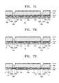
- FIGS. 7A through 7N a method of manufacturing a nozzle plate of an inkjet printhead according to the present invention will be described with reference to FIGS. 7A through 7N.
- FIGS. 7A through 7N are sequential sectional views that illustrate a method of manufacturing a nozzle plate of a piezoelectric inkjet printhead according to the first embodiment shown in FIGS. 3 and 4.
- a nozzle plate 130 is a monocrystalline silicon substrate and has a thickness of about 100-200 ⁇ m, preferably 160 ⁇ m.
- first silicon oxide layers 131a and 131b are respectively formed as insulating layers on lower and upper surfaces of the silicon substrate 130, as shown in FIG. 7A.
- the first silicon oxide layers 131 a and 131b may also be formed by Chemical Vapor Deposition (CVD).
- a photoresist PR is coated on the entire surface of the first silicon oxide layer 131b formed on the upper surface of the silicon substrate 130. Then, the photoresist PR is patterned to define openings 107 for ink guiding portions of nozzles.
- the patterning of the photoresist PR may be performed by known photolithography including exposure and development.
- exposed portions of the first silicon oxide layer 131 b through the openings 107 are wet-etched using the patterned photoresist PR as an etching mask to thereby partially expose an upper surface of the silicon substrate 130. Then, the photoresist PR is stripped.
- the exposed portions of the first silicon oxide layer 131b may also be removed by dry-etching such as Reactive Ion Etching (RIE), instead of wet-etching.
- RIE Reactive Ion Etching
- exposed portions of the silicon substrate 130 are etched to a predetermined depth using the first silicon oxide layer 131b as an etching mask to form ink guiding portions 106a.
- the silicon substrate 130 is anisotropically wet-etched using TMAH (Tetramethyl Ammonium Hydroxide) or KOH (potassium hydroxide) as an etchant, the ink guiding portions 106a may be formed in a square pyramidal shape with slanted sidewalls.
- a photoresist PR is coated on the entire surface of the first silicon oxide layer 131 a formed on a lower surface of the silicon substrate 130. Then, the coated photoresist PR is patterned as shown in FIG. 3 to expose a portion of the first silicon oxide layer 131 a intended for a heater 134. As described above, the photoresist PR can be patterned in a different manner according to the arrangement of the heater 134. Further, portions of the first silicon oxide layer 131 a intended for a temperature detector 138 and nozzle metal layers 136 can also be exposed together with the portion intended for the heater 134.
- a metal material is sputtered on the patterned photoresist PR and the entire exposed portions of the first silicon oxide layer 131 a to form a metal layer M.
- the metal material may be Pt as described above.
- FIG. 7G illustrates the silicon substrate 130 with the heater 134, bonding pads 135, the temperature detector 138, and the nozzle metal layers 136 on the lower surface of the silicon substrate 130.
- the photoresist PR shown in FIG. 7F is lift-off, the photoresist PR and portions of the metal layer M formed on the surface of the photoresist PR are removed and portions of the metal layer M formed on the exposed surface of the first silicon oxide layer 131 a remain.
- the remaining portions of the metal layer M form the heater 134, the bonding pads 135, the temperature detector 138, and the nozzle metal layers 136.
- a second silicon oxide layer 132 is deposited as a protection layer for protecting the heater 134, etc. on the entire lower surface of the resultant structure of FIG. 7G.
- the second silicon oxide layer 132 may be deposited by Plasma Enhanced Chemical Vapor Deposition (PECVD).
- PECVD Plasma Enhanced Chemical Vapor Deposition
- the heater 134, etc. are too thick, smoothness of the second silicon oxide layer 132 may be lowered, thereby affecting subsequent photoresist coating and patterning.
- the second silicon oxide layer 132 can be previously planarized by Chemical Mechanical Polishing (CMP).
- a photoresist PR is coated on the entire surface of the second silicon oxide layer 132 and patterned to form openings 108 corresponding to the ink guiding portions 106a.
- the second silicon oxide layer 132 and the first silicon oxide layer 131 a are sequentially dry-etched through the openings 108 using the photoresist PR as an etching mask and then the photoresist PR is stripped. As a result, the nozzle metal layers 136 and a lower surface of the silicon substrate 130 are exposed through the openings 108.
- FIG. 7K illustrates the silicon substrate 130 with nozzles 106 composed of the ink guiding portions 106a and ink outlets 106b.
- the ink outlets 106b communicating with the ink guiding portions 106a are bored through the exposed portions of the silicon substrate 130 by etching.
- the silicon substrate 130 may be dry-etched by ICP (Inductively Coupled Plasma) using the nozzle metal layers 136 as etching masks.
- ICP Inductively Coupled Plasma
- a photoresist PR is coated on the entire lower surface of the resultant structure of FIG. 7K.
- a dry film photoresist PR is formed on the surface of the second silicon oxide layer 132 by a lamination process using heating and pressing.
- the dry film photoresist PR has the advantage of not entering into the nozzles 106.
- the photoresist PR is patterned to form openings 109 corresponding to the bonding pads 135 of the heater 134.
- portions of the second silicon oxide layer 132 exposed through the openings 109 are etched using the patterned photoresist PR as an etching mask, to form contact holes C through the bonding pads 135 of the heater 134 are exposed.
- contact holes intended for exposure of the bonding pads 139 of the temperature detector 138 shown in FIG. 3 may also be formed together with the contact holes C.
- a good hydrophobic metal material for example Au may be coated on surfaces of the nozzle metal layers 136 to form hydrophobic plating layers 137.
- the hydrophobic plating layers 137 are formed by Au electroplating on surfaces of the previously formed nozzle metal layers 136 used as seed layers.
- the metal material i.e., Au may also be coated on exposed surfaces of the bonding pads 135, the bonding pads 135 are not adversely affected due to conductivity of the metal material coated on the surfaces of the bonding pads 135.
- hydrophobic plating layers 137 is possible even without deposition and patterning of a metal material for formation of a separate seed layer.
- a heater for heating ink is integrally formed with a nozzle plate, thereby simplifying the structure of the inkjet printhead and decreasing a manufacturing cost. Furthermore, since ink in the printhead is heated to a uniform temperature, ejection speed and volume of ink droplets through plural nozzles are maintained uniform, thereby enhancing printing quality.
- a temperature detector for ink temperature detection is integrally formed with a nozzle plate or a piezoelectric actuator, ink temperature can be more accurately detected. Therefore, active and accurate temperature control with respect to change of ink temperature is possible, thereby enhancing printing quality.
- ink ejection performance such as directionality, volume, and ejection speed of ink droplets are enhanced, thereby enhancing printing quality.
- the nozzle metal layer surrounding the nozzle serves as an etching mask for formation of an ink outlet of the nozzle. This enables accurate and easy formation of the ink outlet and formation of the hydrophobic plating layer even without deposition and patterning of a metal material for formation of a separate seed layer.
Landscapes
- Engineering & Computer Science (AREA)
- Manufacturing & Machinery (AREA)
- Chemical & Material Sciences (AREA)
- Crystallography & Structural Chemistry (AREA)
- Materials Engineering (AREA)
- Metallurgy (AREA)
- Organic Chemistry (AREA)
- Inorganic Chemistry (AREA)
- Particle Formation And Scattering Control In Inkjet Printers (AREA)
Applications Claiming Priority (2)
| Application Number | Priority Date | Filing Date | Title |
|---|---|---|---|
| KR10-2004-0013567A KR100537522B1 (ko) | 2004-02-27 | 2004-02-27 | 압전 방식의 잉크젯 프린트헤드와 그 노즐 플레이트의제조 방법 |
| EP05251103A EP1568499B1 (fr) | 2004-02-27 | 2005-02-24 | Tête d'impression à jet d'encre et méthode de fabrication de la plaque à orifices |
Related Parent Applications (2)
| Application Number | Title | Priority Date | Filing Date |
|---|---|---|---|
| EP05251103.7 Division | 2005-02-24 | ||
| EP05251103A Division EP1568499B1 (fr) | 2004-02-27 | 2005-02-24 | Tête d'impression à jet d'encre et méthode de fabrication de la plaque à orifices |
Publications (3)
| Publication Number | Publication Date |
|---|---|
| EP1780017A2 true EP1780017A2 (fr) | 2007-05-02 |
| EP1780017A3 EP1780017A3 (fr) | 2008-12-31 |
| EP1780017B1 EP1780017B1 (fr) | 2010-08-25 |
Family
ID=34747963
Family Applications (2)
| Application Number | Title | Priority Date | Filing Date |
|---|---|---|---|
| EP07101257A Expired - Lifetime EP1780017B1 (fr) | 2004-02-27 | 2005-02-24 | Tête d'imprimante à jet d'encre piézoélectrique |
| EP05251103A Expired - Lifetime EP1568499B1 (fr) | 2004-02-27 | 2005-02-24 | Tête d'impression à jet d'encre et méthode de fabrication de la plaque à orifices |
Family Applications After (1)
| Application Number | Title | Priority Date | Filing Date |
|---|---|---|---|
| EP05251103A Expired - Lifetime EP1568499B1 (fr) | 2004-02-27 | 2005-02-24 | Tête d'impression à jet d'encre et méthode de fabrication de la plaque à orifices |
Country Status (5)
| Country | Link |
|---|---|
| US (1) | US7445314B2 (fr) |
| EP (2) | EP1780017B1 (fr) |
| JP (1) | JP4727257B2 (fr) |
| KR (1) | KR100537522B1 (fr) |
| DE (2) | DE602005007947D1 (fr) |
Families Citing this family (41)
| Publication number | Priority date | Publication date | Assignee | Title |
|---|---|---|---|---|
| ATE470571T1 (de) * | 2004-05-03 | 2010-06-15 | Fujifilm Dimatix Inc | Biegsame druckkopfleiterplatte |
| KR100757861B1 (ko) * | 2004-07-21 | 2007-09-11 | 삼성전자주식회사 | 잉크젯 헤드 기판, 잉크젯 헤드 및 잉크젯 헤드 기판의제조방법. |
| JP4771042B2 (ja) * | 2004-07-23 | 2011-09-14 | ゲットナー・ファンデーション・エルエルシー | 圧電素子搭載装置、およびこれを用いた液滴吐出装置、画像出力装置 |
| US7438395B2 (en) * | 2004-09-24 | 2008-10-21 | Brother Kogyo Kabushiki Kaisha | Liquid-jetting apparatus and method for producing the same |
| KR100612888B1 (ko) * | 2005-01-28 | 2006-08-14 | 삼성전자주식회사 | 온도 센서를 가진 압전 방식의 잉크젯 프린트헤드와잉크젯 프린트헤드에 온도 센서를 부착하는 방법 |
| JP4810192B2 (ja) * | 2005-11-01 | 2011-11-09 | キヤノン株式会社 | インクジェット記録ヘッドの製造方法、及びインクジェット記録ヘッド |
| KR100745758B1 (ko) * | 2006-01-21 | 2007-08-02 | 삼성전자주식회사 | 압전 액츄에이터를 채용한 잉크젯 프린트헤드 |
| JP5453808B2 (ja) * | 2006-04-27 | 2014-03-26 | コニカミノルタ株式会社 | 活性光線硬化型組成物、活性光線硬化型インクジェットインク、該活性光線硬化型インクジェットインクを用いた画像形成方法及びインクジェット記録装置 |
| US20070263038A1 (en) * | 2006-05-12 | 2007-11-15 | Andreas Bibl | Buried heater in printhead module |
| JP4973377B2 (ja) * | 2006-08-23 | 2012-07-11 | ブラザー工業株式会社 | 液体移送装置及び液体移送装置の製造方法 |
| US8220905B2 (en) | 2006-08-23 | 2012-07-17 | Brother Kogyo Kabushiki Kaisha | Liquid transporting apparatus and method of producing liquid transporting apparatus |
| KR101366076B1 (ko) * | 2007-10-11 | 2014-02-21 | 삼성전자주식회사 | 잉크젯 프린팅 장치 및 그 구동방법 |
| JP4582173B2 (ja) * | 2008-03-28 | 2010-11-17 | ブラザー工業株式会社 | 液体移送装置 |
| US20100110144A1 (en) * | 2008-10-31 | 2010-05-06 | Andreas Bibl | Applying a Layer to a Nozzle Outlet |
| JP2010149510A (ja) * | 2008-11-20 | 2010-07-08 | Canon Inc | 記録素子基板、記録素子基板を備えた記録ヘッド |
| JP5271070B2 (ja) * | 2008-12-24 | 2013-08-21 | エスアイアイ・プリンテック株式会社 | ヘッドチップ、液体噴射ヘッド及び液体噴射装置 |
| KR101069412B1 (ko) | 2009-01-21 | 2011-10-04 | 삼성전기주식회사 | 잉크젯 헤드 |
| US8876242B2 (en) * | 2009-05-08 | 2014-11-04 | Canon Kabushiki Kaisha | Liquid ejection head |
| US8177338B2 (en) * | 2009-12-10 | 2012-05-15 | Xerox Corporation | High frequency mechanically actuated inkjet |
| JP5743070B2 (ja) * | 2011-03-23 | 2015-07-01 | セイコーエプソン株式会社 | 液体噴射ヘッド及び液体噴射装置 |
| JP5904395B2 (ja) * | 2011-07-14 | 2016-04-13 | 株式会社リコー | 液滴吐出ヘッド、インクカートリッジ及び画像形成装置 |
| US8585185B2 (en) * | 2011-09-22 | 2013-11-19 | Xerox Corporation | High density electrical interconnect using limited density flex circuits |
| US8727508B2 (en) * | 2011-11-10 | 2014-05-20 | Xerox Corporation | Bonded silicon structure for high density print head |
| KR102016579B1 (ko) * | 2012-06-19 | 2019-09-02 | 삼성디스플레이 주식회사 | 잉크젯 프린트 헤드 및 이의 제조 방법 |
| JP2014046665A (ja) * | 2012-09-04 | 2014-03-17 | Canon Inc | 液体吐出ヘッドの製造方法 |
| US9636028B2 (en) * | 2013-11-08 | 2017-05-02 | Neuronexus Technologies, Inc. | Three-dimensional neural probe microelectrode array and method of manufacture |
| WO2015096545A1 (fr) | 2013-12-26 | 2015-07-02 | 大连理工大学 | Tête à jet de liquide et appareil de pulvérisation de liquide |
| JP6447051B2 (ja) * | 2014-03-18 | 2019-01-09 | 株式会社リコー | 液体吐出ヘッド、液体吐出ヘッドの製造方法、画像形成装置 |
| CN104943179A (zh) * | 2015-07-01 | 2015-09-30 | 西北工业大学(张家港)智能装备技术产业化研究院有限公司 | 一种3d打印用的压电喷头 |
| JP6953752B2 (ja) * | 2017-03-15 | 2021-10-27 | ブラザー工業株式会社 | 液体吐出ヘッド及びその製造方法 |
| JP6920848B2 (ja) * | 2017-03-24 | 2021-08-18 | 東芝テック株式会社 | 液体吐出ヘッド及び液体吐出装置 |
| JP7094693B2 (ja) * | 2017-11-27 | 2022-07-04 | キヤノン株式会社 | 液体吐出ヘッドの製造方法及び液体吐出ヘッド |
| WO2020159517A1 (fr) * | 2019-01-31 | 2020-08-06 | Hewlett-Packard Development Company, L.P. | Puce fluidique avec surveillance de condition de surface |
| US20240085288A1 (en) | 2021-01-11 | 2024-03-14 | Vib Vzw | Means and methods for time-resolved sampling |
| JP2023042734A (ja) * | 2021-09-15 | 2023-03-28 | エスアイアイ・プリンテック株式会社 | 液体噴射ヘッド及び液体噴射記録装置 |
| JP7795715B2 (ja) * | 2022-02-07 | 2026-01-08 | 株式会社リコー | 液体吐出ヘッド、液体吐出ユニット、及び、液体を吐出する装置 |
| JP7823418B2 (ja) * | 2022-02-09 | 2026-03-04 | セイコーエプソン株式会社 | 液体吐出ヘッド、及び、液体吐出装置 |
| KR20240017222A (ko) * | 2022-07-28 | 2024-02-07 | 삼성디스플레이 주식회사 | 잉크젯 헤드 및 이를 포함하는 잉크젯 프린팅 장치 |
| JP2024098207A (ja) * | 2023-01-10 | 2024-07-23 | セイコーエプソン株式会社 | 液体吐出装置の駆動方法 |
| JP2024098208A (ja) * | 2023-01-10 | 2024-07-23 | セイコーエプソン株式会社 | 液体吐出装置の駆動方法 |
| WO2026082781A1 (fr) | 2024-10-15 | 2026-04-23 | Vib Vzw | Moyens et procédés de pulvérisation de microgouttelettes à partir d'une puce |
Citations (2)
| Publication number | Priority date | Publication date | Assignee | Title |
|---|---|---|---|---|
| EP0900657A2 (fr) | 1997-09-08 | 1999-03-10 | Konica Corporation | Imprimante à jet d'encre |
| US6074033A (en) | 1997-03-12 | 2000-06-13 | Seiko Epson Corporation | Device for driving inkjet print head |
Family Cites Families (22)
| Publication number | Priority date | Publication date | Assignee | Title |
|---|---|---|---|---|
| DE3717294C2 (de) * | 1986-06-10 | 1995-01-26 | Seiko Epson Corp | Tintenstrahlaufzeichnungskopf |
| US4847630A (en) * | 1987-12-17 | 1989-07-11 | Hewlett-Packard Company | Integrated thermal ink jet printhead and method of manufacture |
| JP2658204B2 (ja) * | 1988-06-30 | 1997-09-30 | 富士ゼロックス株式会社 | インクジェット記録装置 |
| JPH04338546A (ja) * | 1991-05-15 | 1992-11-25 | Fujitsu Ltd | インクジェットヘッド |
| US5308442A (en) * | 1993-01-25 | 1994-05-03 | Hewlett-Packard Company | Anisotropically etched ink fill slots in silicon |
| US5659346A (en) | 1994-03-21 | 1997-08-19 | Spectra, Inc. | Simplified ink jet head |
| JPH0858084A (ja) * | 1994-08-24 | 1996-03-05 | Brother Ind Ltd | インクジェットヘッド |
| TW426613B (en) * | 1996-01-23 | 2001-03-21 | Seiko Epson Corp | Ink jet printer head, its manufacturing method and ink |
| JPH09272207A (ja) * | 1996-04-05 | 1997-10-21 | Sony Corp | プリントヘツドの製造方法 |
| DE19806807A1 (de) * | 1997-02-19 | 1998-09-03 | Nec Corp | Tröpfchenausstoßvorrichtung |
| JP2927266B2 (ja) * | 1997-02-19 | 1999-07-28 | 日本電気株式会社 | 液滴噴射装置 |
| JP2000203033A (ja) * | 1999-01-19 | 2000-07-25 | Ricoh Co Ltd | ノズル形成部材及びインクジェットヘッド並びにその製造方法 |
| US6345880B1 (en) * | 1999-06-04 | 2002-02-12 | Eastman Kodak Company | Non-wetting protective layer for ink jet print heads |
| KR100361081B1 (ko) * | 1999-10-29 | 2002-11-18 | 삼성전자 주식회사 | 반도체 소자의 커패시터 제조방법 |
| US6523943B1 (en) * | 1999-11-01 | 2003-02-25 | Kansai Research Institute, Inc. | Piezoelectric element, process for producing the piezoelectric element, and head for ink-jet printer using the piezoelectric element |
| JP2001310472A (ja) * | 2000-04-28 | 2001-11-06 | Fuji Photo Film Co Ltd | 画像形成装置 |
| KR100397604B1 (ko) * | 2000-07-18 | 2003-09-13 | 삼성전자주식회사 | 버블 젯 방식의 잉크 젯 프린트 헤드 및 그 제조방법 |
| US6533395B2 (en) * | 2001-01-18 | 2003-03-18 | Philip Morris Incorporated | Inkjet printhead with high nozzle to pressure activator ratio |
| JP3920596B2 (ja) * | 2001-06-25 | 2007-05-30 | 東芝テック株式会社 | インクジェット記録装置及びインクジェット記録方法 |
| KR100453047B1 (ko) * | 2002-04-17 | 2004-10-15 | 삼성전자주식회사 | 잉크 젯 프린트 헤드 및 이의 제조 방법 |
| KR100493160B1 (ko) * | 2002-10-21 | 2005-06-02 | 삼성전자주식회사 | 테이퍼 형상의 노즐을 가진 일체형 잉크젯 프린트헤드 및그 제조방법 |
| KR100519759B1 (ko) * | 2003-02-08 | 2005-10-07 | 삼성전자주식회사 | 잉크젯 프린트헤드 및 그 제조방법 |
-
2004
- 2004-02-27 KR KR10-2004-0013567A patent/KR100537522B1/ko not_active Expired - Fee Related
-
2005
- 2005-02-24 DE DE602005007947T patent/DE602005007947D1/de not_active Expired - Lifetime
- 2005-02-24 EP EP07101257A patent/EP1780017B1/fr not_active Expired - Lifetime
- 2005-02-24 EP EP05251103A patent/EP1568499B1/fr not_active Expired - Lifetime
- 2005-02-24 DE DE602005023175T patent/DE602005023175D1/de not_active Expired - Lifetime
- 2005-02-25 JP JP2005052080A patent/JP4727257B2/ja not_active Expired - Fee Related
- 2005-02-25 US US11/064,834 patent/US7445314B2/en not_active Expired - Fee Related
Patent Citations (2)
| Publication number | Priority date | Publication date | Assignee | Title |
|---|---|---|---|---|
| US6074033A (en) | 1997-03-12 | 2000-06-13 | Seiko Epson Corporation | Device for driving inkjet print head |
| EP0900657A2 (fr) | 1997-09-08 | 1999-03-10 | Konica Corporation | Imprimante à jet d'encre |
Also Published As
| Publication number | Publication date |
|---|---|
| DE602005007947D1 (de) | 2008-08-21 |
| EP1780017B1 (fr) | 2010-08-25 |
| EP1780017A3 (fr) | 2008-12-31 |
| DE602005023175D1 (de) | 2010-10-07 |
| KR20050087642A (ko) | 2005-08-31 |
| JP2005238846A (ja) | 2005-09-08 |
| JP4727257B2 (ja) | 2011-07-20 |
| EP1568499A1 (fr) | 2005-08-31 |
| US7445314B2 (en) | 2008-11-04 |
| US20050190232A1 (en) | 2005-09-01 |
| EP1568499B1 (fr) | 2008-07-09 |
| KR100537522B1 (ko) | 2005-12-19 |
Similar Documents
| Publication | Publication Date | Title |
|---|---|---|
| EP1780017B1 (fr) | Tête d'imprimante à jet d'encre piézoélectrique | |
| US5278585A (en) | Ink jet printhead with ink flow directing valves | |
| EP1813428B1 (fr) | Tête d'impression piézoélectrique à jet d'encre et méthode de fabrication | |
| EP1652673B1 (fr) | Plaque à orifices, tête d'impression par jet d'encre l'utilisant, et sa méthode de fabrication | |
| EP1848592B1 (fr) | Module de tete d'impression | |
| CN101489794B (zh) | 打印头模块中的埋入式加热器及打印头本体 | |
| KR100560593B1 (ko) | 액체 토출 헤드의 제조방법 | |
| US6649074B2 (en) | Bubble-jet type ink-jet print head and manufacturing method thereof | |
| EP1568501B1 (fr) | Dispositif d'actionnement piézoélectrique pour tête d'impression jet d'encre et son procédé de fabrication | |
| KR100641357B1 (ko) | 잉크젯 프린트 헤드 및 그 제조 방법 | |
| KR100682917B1 (ko) | 압전 방식의 잉크젯 프린트헤드 및 그 제조방법 | |
| KR100446634B1 (ko) | 잉크젯 프린트헤드 및 그 제조방법 | |
| KR100561866B1 (ko) | 압전 방식 잉크젯 프린트헤드 및 그 제조방법 | |
| CN108136776A (zh) | 流体喷射设备 | |
| CN101124093A (zh) | 打印头模块 | |
| US20080122899A1 (en) | Inkjet print head and method of manufacturing the same | |
| KR100528349B1 (ko) | 압전 방식의 잉크젯 프린트헤드 및 그 제조방법 | |
| KR100421027B1 (ko) | 잉크젯 프린트헤드 및 그 제조방법 | |
| JPH07205426A (ja) | インクジェットプリントヘッド及びサーマルインクジェットプリントヘッドの製造方法 |
Legal Events
| Date | Code | Title | Description |
|---|---|---|---|
| PUAI | Public reference made under article 153(3) epc to a published international application that has entered the european phase |
Free format text: ORIGINAL CODE: 0009012 |
|
| AC | Divisional application: reference to earlier application |
Ref document number: 1568499 Country of ref document: EP Kind code of ref document: P |
|
| AK | Designated contracting states |
Kind code of ref document: A2 Designated state(s): DE FR GB |
|
| RIN1 | Information on inventor provided before grant (corrected) |
Inventor name: CHUNG, JAE-WOO Inventor name: LIM, SEUNG-MO Inventor name: KIM, JONG-BEOM408-704 JUGONG APT. Inventor name: LEE, JAE-CHANG Inventor name: OH, JUNG-MIN |
|
| RIN1 | Information on inventor provided before grant (corrected) |
Inventor name: KIM, JONG-BEOM408-704 JUGONG APT. Inventor name: LEE, JAE-CHANG Inventor name: CHUNG, JAE-WOO Inventor name: OH, JUNG-MIN Inventor name: LIM, SEUNG-MO |
|
| RIN1 | Information on inventor provided before grant (corrected) |
Inventor name: CHUNG, JAE-WOO Inventor name: OH, JUNG-MIN Inventor name: LIM, SEUNG-MO Inventor name: LEE, JAE-CHANG Inventor name: KIM, JONG-BEOM408-704 JUGONG APT. |
|
| PUAL | Search report despatched |
Free format text: ORIGINAL CODE: 0009013 |
|
| AK | Designated contracting states |
Kind code of ref document: A3 Designated state(s): DE FR GB |
|
| RIC1 | Information provided on ipc code assigned before grant |
Ipc: B41J 2/16 20060101ALI20081127BHEP Ipc: B41J 2/14 20060101AFI20081127BHEP |
|
| 17P | Request for examination filed |
Effective date: 20090625 |
|
| AKX | Designation fees paid |
Designated state(s): DE FR GB |
|
| GRAP | Despatch of communication of intention to grant a patent |
Free format text: ORIGINAL CODE: EPIDOSNIGR1 |
|
| RAP1 | Party data changed (applicant data changed or rights of an application transferred) |
Owner name: SAMSUNG ELECTRO-MECHANICS CO., LTD. |
|
| GRAS | Grant fee paid |
Free format text: ORIGINAL CODE: EPIDOSNIGR3 |
|
| GRAA | (expected) grant |
Free format text: ORIGINAL CODE: 0009210 |
|
| AC | Divisional application: reference to earlier application |
Ref document number: 1568499 Country of ref document: EP Kind code of ref document: P |
|
| AK | Designated contracting states |
Kind code of ref document: B1 Designated state(s): DE FR GB |
|
| REG | Reference to a national code |
Ref country code: GB Ref legal event code: FG4D |
|
| REF | Corresponds to: |
Ref document number: 602005023175 Country of ref document: DE Date of ref document: 20101007 Kind code of ref document: P |
|
| PLBE | No opposition filed within time limit |
Free format text: ORIGINAL CODE: 0009261 |
|
| STAA | Information on the status of an ep patent application or granted ep patent |
Free format text: STATUS: NO OPPOSITION FILED WITHIN TIME LIMIT |
|
| 26N | No opposition filed |
Effective date: 20110526 |
|
| REG | Reference to a national code |
Ref country code: DE Ref legal event code: R097 Ref document number: 602005023175 Country of ref document: DE Effective date: 20110526 |
|
| REG | Reference to a national code |
Ref country code: FR Ref legal event code: PLFP Year of fee payment: 12 |
|
| PGFP | Annual fee paid to national office [announced via postgrant information from national office to epo] |
Ref country code: DE Payment date: 20160120 Year of fee payment: 12 |
|
| PGFP | Annual fee paid to national office [announced via postgrant information from national office to epo] |
Ref country code: FR Payment date: 20160126 Year of fee payment: 12 Ref country code: GB Payment date: 20160121 Year of fee payment: 12 |
|
| REG | Reference to a national code |
Ref country code: DE Ref legal event code: R119 Ref document number: 602005023175 Country of ref document: DE |
|
| GBPC | Gb: european patent ceased through non-payment of renewal fee |
Effective date: 20170224 |
|
| REG | Reference to a national code |
Ref country code: FR Ref legal event code: ST Effective date: 20171031 |
|
| PG25 | Lapsed in a contracting state [announced via postgrant information from national office to epo] |
Ref country code: FR Free format text: LAPSE BECAUSE OF NON-PAYMENT OF DUE FEES Effective date: 20170228 Ref country code: DE Free format text: LAPSE BECAUSE OF NON-PAYMENT OF DUE FEES Effective date: 20170901 |
|
| PG25 | Lapsed in a contracting state [announced via postgrant information from national office to epo] |
Ref country code: GB Free format text: LAPSE BECAUSE OF NON-PAYMENT OF DUE FEES Effective date: 20170224 |